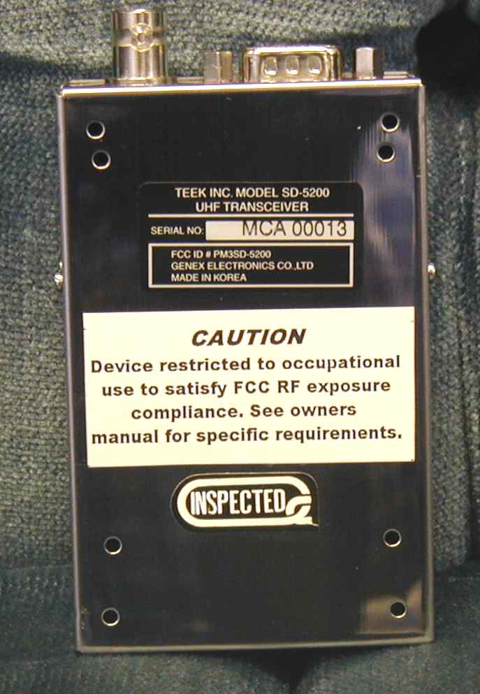
PM3SD5200RF Data Radio Transceiver
Genex Telecom Co., Ltd.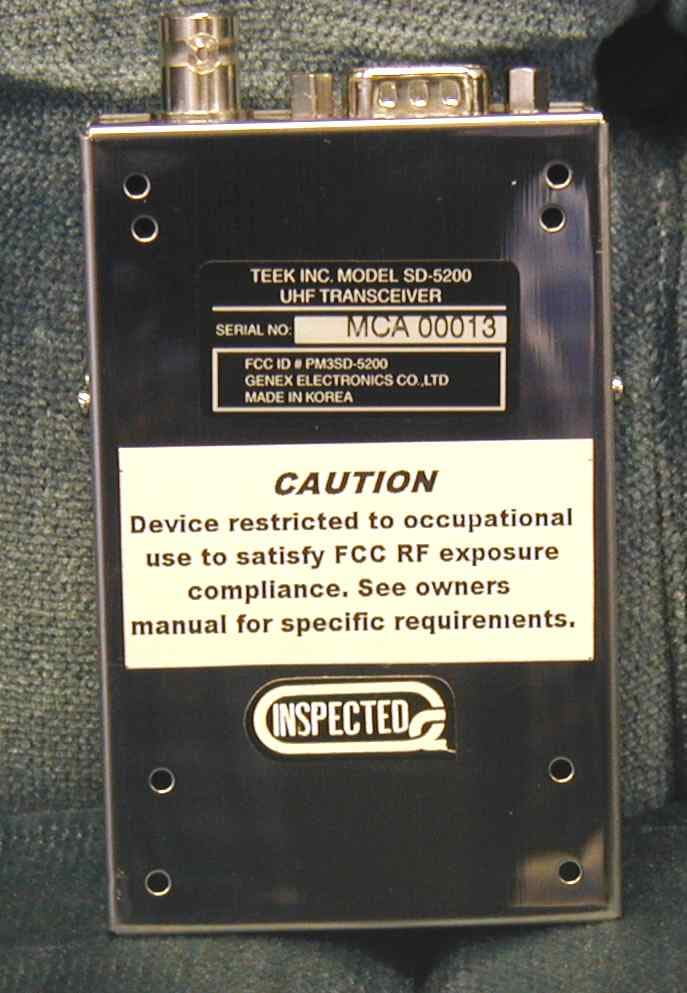
Click to zoom
Application Details
- Equipment Class
- TNB - Licensed Non-Broadcast Station Transmitter
- Date of Grant
- Sep 23, 2002
- Application Purpose
- Original Equipment
- Date of Application
- Sep 23, 2002
- Equipment Note
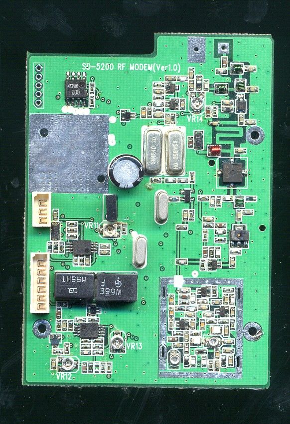
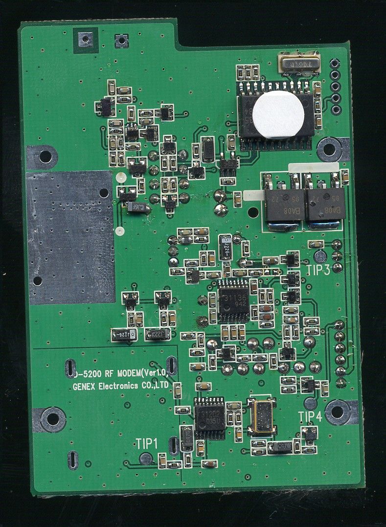
- RF Data Radio Transceiver
- Frequency Range
- 450.00000000 - 470.00000000
- Company
- Genex Telecom Co., Ltd.
- Country
- South Korea
Documents & Files
Document Text
Text extracted from the exhibit documents filed with the FCC. Open a document above to read the original.
Users Manual
TEKK INC. SD-5200 MANUAL 5/2 WATT RF DATA RADIO IMPORTANT NOTICE! FCC RF Exposure Compliance requirements for Occupational Use: • This device must be restricted to work related operations in an occupational / controlled RF exposure environment. • Transmitting duty factor may not exceed 50%. • All qualified users must have the knowledge to control their own, passengers and bystanders’RF exposure to comply with the General Population / Controlled MPE limit and requirements. • The antenna used for this transmitter must be installed to provide a separation distance of at least 32cm from all persons and must not exceed an antenna gain of 0 dDd. IMPORTANT NOTICE! This radio can only be programmed to frequency by qualified, approved technicians using a separate PC software and cable package. Only authorized technicians can contact Tekk to purchase this programming software product. CH.1 PRODUCT INTRODUCTION SD-5200, This RF Data Radio is designed to operate in the frequency range is 450MHz~ 470MHz. Inside of SD-5200 is installed microprocessor and SD-5200 is operated by PLL type. RF power is 2watt and 5watt. Bandwidth is 12.5khz or 25khz SD-5200 features -. PLL SYNTHESIZER type -. set parameter with PC program -. RF power : 2 Watt, 5Watt -. band width : 12.5/25kHz -. light weight -. PC downloading -. Power : DC 10V 2. SD-5200 outward view Data Radio (SD-5200) 3. D-SUB Connector PIN Specification PIN NO PIN Specification Remark 1 DC+12V 9V~15V 2 GND 3 PTT “Low" Active 4 DATA INPUT 5 DATA OUTPUT 6 S_I/O( PC Program) Programming 7 GND 8 RSSI Receive Signal Strength Indicator 9 S.Q(CD) Carrier Detect 4. CON2 PIN Specification (PCB Connector) PIN NO PIN Specification Remark 1 RSSI Receive Signal Strength Indicator 2 GND 3 S_I/O PC Program PIN 5. CON3 PIN Specification (PCB Connector) 6. CON4 PIN Specification (PCB Connector) CH2. SPECIFICATIONS PIN NO PIN Specification Remark 1 S.Q (C.D) 2 DATA INPUT 3 DATA OUTPUT 4 PTT 5 DC+12V 6 GND PIN NO PIN Specification Remark 1 RESET 2 DC+5V 3 S_CLOCK 4 S_DATA 5 GND used for modifying MPU Program 1. Specification GENERAL Operating Mode Frequency Range Frequency Stability Programmable Channels Channel Spacing Dimensions Weight Power Source Current Drain(maximum) Conventional (nontrunked) only 450~470MHz ±2.5PPM(-30 to +60?) 1 Channel Dual Channel Spacing 12.5/25kHz 30mm(H)×60mm(W)×95mm(L) 360g DC 9~15V Transmit mode - 1.8A RECEIVER Sensitivity Squelch Sensitiviy Selectivity Spurious and Harmonic Rejection Intermodulation FM Hum and Noise Maximum Frequency Spread Audio Output Power Audio Distortion Audio Response IF Frequencies Input Impedance .35uV 12 dB SINAD .25uV 10dB SINAD -60dB (12.5KHz) -60dB (25KHz) -60dB -60dB -34dB(12.5KHz), -40dB(25KHz) UHF = 20MHz 460mW across an 8-ohm load Less than 5% at rated output ±2dB from characteristic from 20~3000Hz 21.4MHz and 455kHz 50 ohms TRANSMITTER RF Power Output Spurious and Harmonic FM Hum and Noise Audio Distortion Audio Frequency Response Maximum Channel Spread Output Impedance 2 Watt or 5 Watt -60 -34dB(12.5KHz), -40dB(25KHz) 5% maximum with 1kHz modulation ±2dB from characteristic from 20~3000Hz UHF = 20MHz 50 ohms CH. 3 SD-5200 circuit 1. SD-5200 circuit SD-5200 circuit is composed of RF and MPU. (RF determines communication quality and performance. MPU controls terminal performance.) RF is composed of TX and RX. TX is composed of synthesizer (Synthesizer generates TX frequency.), VCO, Data ALC (Automatic Level Control), Power Drive, final amplification and antenna switch. RX is composed of front-end, mixer, local drive, and crystal filter. IF amplifier, IF IC and Data conduct. MPU is composed of EEPROM storing parameter of controls in the SD-5200. 2. Transmit 2.1 SYNTHESIZER Synthesizer is consisting of TCXO, PLL IC, Charge Pump, LPF and VCO. See illustration 2-1. TCXO (U17) plays a key role to make usable frequency for terminal and uses a 14.4MHz(-30?C~+60?C, 2.5ppm) of VX-23VA in JVC co. It uses resistance R65, R66 and VR13 externally for accuracy of frequency and modulation of low frequency data signal. When VR13 is turned to '+', voltage increases and frequency lowers. When VR13 is turned to '-', frequency rises. If TX or RX frequency deviation occurs, you can control with VR13. Inside of PLL IC, there are 4 Divider Registers (CH1, CH2 Programmable Divider, Reference Divider and Option Control). Now, SD-2000N/5200 use only CH1 Programmable Divider 2.1.1 Composition of Divider Register Inside of PLL IC consistsof 4 Registers and is set with code. 14.4MHz f R TCXO U104 Reference Counter f V Loop Filter VCO 64 Prescaler N Counter Phase Detector A Counter Illustration 2-1 Composition of Synthesizer COD E ITEM 1 0 Number of dividers by CH1 Programmable divider(Fin1) 0 1 Number of dividers by CH2 Programmable divider(Fin2) 1 1 Number of dividers by reference divider(Xin) 0 0 Option control 1) Programmable divider LSB MSB A0 A1 A2 A3 A4 D0 D1 D2 D3 D4 D5 D6 D7 D8 D9 D10 D11 1 0 Calculation for generating 450.0125 MHz frequency, as below. Set basic channel as 6.25 KHz. 450.0125 MHz ÷ 6.25 KHz = 72002 N and A Counter values are 72002 ÷ 64 = 1125. 03125 N value = 1125 ? 465 hex A value = 0.3125 ? 0.3125 x 64 = 20 ? 14 hex LSB 4 1 5 6 4 MSB 2) Reference Divider LSB MSB Calculation for basic frequency of 6.25 KHz with TCXO frequency 14.4 MHz ÷ 6.25 KHz = 2304 ? 900 hex 0 0 1 0 1 1 0 1 0 0 1 1 0 0 0 1 0 1 0 D0 D1 D2 D3 D4 D5 D6 D7 D8 D9 D10 D11 1 1 LSB 0 0 9 MSB 3) Option Control T CP CP1 CP2 SB1 CP1 CP2 SB2 SBR LD1 LD2 SW 0 0 T : Test Mode (always "0") CP : Charge pump output polarity CP Output Polarity 0 Normal 1 Reverse Charge Pump Output Current Lock detector output Control bit SB1 SB2 LD1 LD2 Lock detector output state 0 0 L 0 1 CH2 only detector 1 0 CH1 only detector 0 0 1 1 CH1, CH2 0 0 L 0 1 H 0 0 0 0 0 0 0 0 1 0 0 1 1 1 Control bit CP1 CP2 Charge pump output current 0 0 100 μA 0 1 200 μA 1 0 400 μA 0 0 800 μA 1 0 CH2 only detector 1 1 CH1 only detector 0 0 L 0 1 CH2 only detector 1 0 H 1 0 1 1 CH1 only detect…
Text truncated - open the document above for the full version.
Block Diagram
BLOCK_DIAGRAM.sch-1 - Fri May 17 17:27:03 2002
Operational Description
FK1 6 VG08533 flufxlw 41 VG08533 flufxlw VG08533 flufxlw lv frpsrvhg ri UI dqg PSX1 +UI ghwhuplqhv frppxqlfdwlrq txdolw| dqg shuirupdqfh1 PSX frqwurov whuplqdo shuirupdqfh1, UI lv frpsrvhg ri W[ dqgU[1 W[ lv frpsrvhg ri v|qwkhvl}hu+V|qwkhvl}hu jhqhudwh W[ iuhtxhqf|1,/ YFR/ GdwdDOF+Dxwrpdwlf Ohyho Frqwuro,/ Srzhu Gulyh/ ilqdodpsolilfdwlrq dqg dqwhqqd vzlwfk1 U[ lv frpsrvhg ri iurqw0hqg/ pl{hu/ orfdo gulyh/ fu|vwdo ilowhu1 LI dpsolilhu/ LI LF dqg Gdwd frqgxfw1 PSX lv frpsrvhg ri HHSURP vwrulqj sdudphwhu ri hyhu| nlqg dqg frqwurov VG085331 51 Wudqvplw 514 V\QWKHVL]HU V|qwkhvl}hu lv frqvlvw ri WF[R/ SOO LF/ Fkdujh Sxps/ OSI dqg YFR1 Vhh looxvwudwlrq 5041 WF[R+X4:, sod|v d nh| uroh wr pdnh xvdeoh iuhtxhqf| iru whuplqdo dqg xvh 4717PK}+063㏃F 㐤.93㏃F/ 518ssp, ri Y[056YD lq MYF fr1 Lw xvhv uhvlvwdqfh U98/ U99 dqg YU46 h{whuqdoo| iru dffxudf| ri iuhtxhqf| dqg prgxodwlrq ri orz iuhtxhqf| gdwd vljqdo1 ZkhqYU46lvwxuqhg wr *.*/ yrowdjh lqfuhdvhv dqg iuhtxhqf| orzhuv1 Zkhq YU46 lv wxuqhg wr *0*/iuhtxhqf| ulvhv1 Li W[ ru U[ iuhtxhqf| ghyldwlrq rffxu/ |rx fdq frqwuro zlwk YU461 Lqvlgh ri SOO LF/ wkhuh duh 7 Glylghu Uhjlvwhuv+FK4/ FK5 Surjudppdeoh Glylghu/ Uhihuhqfh Glylghu dqg Rswlrq Frqwuro,1 Qrz/ VG05333Q28533 xvh rqo| FK4 Surjudppdeoh Glylghu CODEITEM 10Number of dividers by CH1 Programmable divider(Fin1) 01Number of dividers by CH2 Programmable divider(Fin2) 11Number of dividers by reference divider(Xin) 00Option control A0A1A2A3A4D0D1D2D3D4D5D6D7D8D9D10D1110 D0D1D2D3D4D5D6D7D8D9D10D1111 TCPCP1CP2SB1CP1CP2SB2SBRLD1LD2SW00 0010110100110001010 00000000100111 CP 0Normal 1Reverse 51414 Fspsrvlwlrq ri Glylghu Uhjlvwhu Lqvlgh ri SOO LF lv frqvlvw ri 7 Uhjlvwhuv dqg lv vhw zlwk frgh1 4, Surjudppdeoh glylghu OVEPVE Fdofxodwlrq iru jhqhudwlqj 78313458 PK} iuhtxhqf|/ dv ehorz1 Vhwedvlffkdqqhodv9158NK}1 78313458 PK} 1日 9158 NK} @ :5335 Q dqg D Frxqwru ydoxhv duh :5335 1日 97 @ 44581 36458 Q ydoxh @ 4458 㐆 798 kh{ D ydoxh @ 316458 㐆 316458 { 97 @ 53 㐆 47 kh{ OVE74897PVE 5, Uhihuhqfh Glylghu OVEPVE Fdofxodwlrq iru edvlf iuhtxhqf|ri 9158 NK} zlwk WF[R iuhtxhqf| 4717 PK} 1日 9158 NK} @ 5637 㐆 <33 kh{ OVE33<PVE 6, Rswlrq Frqwuro W= Whvw Prgh +dozd|v %3%, FS= Fkdujh sxps rxwsxw srodulw| Control bit CP1CP2 00±μ 01±μ 10±μ 00±μ Control bit Lock detector output state SB1SB2LD1LD2 00 00L 01CH2 only detector 10CH1 only detector 11CH1, CH2 01 00L 01H 10CH2 only detector 11CH1 only detector 10 00L 01CH2 only detector 10H 11CH1 only detector 11 00L 01H 10H 11H SWOutput 0OFF 1ON 00110001010000 Fkdujh Sxps Rxwsxw Fxuuhqw Orfn ghwhfwru rxwsxw Ilowhu Vzlwfk Frqwuro Rq FK4/ gdwd iru fkhfnlqj SOO Orfn/ dv ehorz1 515YFR YFR lv flufxlw zlwk Froslwwv Rvfloodwru/ rvfloodwhv zlwk frqwuro yrowdjhe| v|qwkhvl}hu dqg frqvlvwriW[dqgU[1 U[ YFR lv rshudwlqj zkhq U[ YFR srzhu Vzlwfk/ WU+T5;, wxuqv rq1 W[ YFR lv rshudwlqj zkhq W[ YFR srzhu Vzlwfk/ WU+T5:, wxuqv rq1Frqwuro yrowdjh riYFR fkdqjh sxovh yrowdjh jhqhudwhg lq Fkdujh Sxps ri SOO LF wr GF yrowdjh dv sdvvlqj Orz Sdvv Ilowhu +F:3/ F:4/ F:5/ U9</ U:3,1 Iuhtxhqf| udqjh e| frqwuro srzhu/ dv wdeoh 614 wdeoh614, Frqwuro srzhu dqg iuhtxhqf| PRGHOSOO Frqwuro Srzhu Udqjhiuhtxhqf| udqjhuhpdun VG08533 W[416718Y783 7:3 PK} U[416718Y75;19 77;19PK} Rshudwlrq iru wudqvplw Prgh lv rvfloodwhg e| T54/ F;7/ F;8/ F;9/ F;:/ F;;/ F;</ F<3/ F<4/ YF45/ G48/ G49 dqg O59+Wkh| duh frqvlvw ri Froslwwv Rvfloodwru1,1 U: dqg F;9 duh flufxlw wr uhpdlq 783 7:3 PK} iuhtxhqf| vwdeoh1 Ydulfds Glrgh ghwhuplqhv iuhtxhqf| udqjh iru G481G49 dowhuv Gdwd1 Rshudwlrq iru Uhfhlyh Prgh lv rvfloodwhg e| T53/ F:6/ F:7/ F:8/ F:9/ F::/ F:;/ F:</ G47 dqg O541 T55 dqg h{wud sduwv duh exiihuv wr dpsoli| UI fduulhu zklfk lv rvfloodwhg e|W[ YFR dqg U[ YFR/ uhpdlq ilqdo rxwsxw 3gE p ㏞5gE dqg suhyhqw dpsolilhg uhyhuvh srzhu iurp rxwsxw sduw1 516 Lqsxw Gdwd DOF+Dxwrpdwlf Ohyho Frqwuro, Xvhu fdq xvh gliihuhqw lqsxw vljqdo ohyho1 Lqsxw Gdwd DOF+DxwrpdwlfOhyho Frqwuro, lv ghvljqhg wr xvh hyhu| gljlwdo vljqdo zkrvh lqsxw vljqdo udqjh lv 38Y319Y1 Lqsxwvljqdogdwdsurylghge|G0vxeFrqqhfwruQr17slqdpsoli|7:wlphvdvX49D dqg lv surylghg wrX49E Olplwlqj flufxlw1 Rxwsxw ri X49E uhvwulfwv hyhu| vljqdo dv 417Y dqg surylgh wr YFR dqg WF[R1 WF[R+X4:, dowhuv gdwd vljqdo+3683K}, zlwkU96 dqg F97 dqg grhv qrw dowhu pruh wkdq 683K} zlwk YFR1 U93 lv xvhg dv e|sdvv/ qrwxvlqjlqsxwGdwdDOF+DxwrpdwlfOhyho Frqwuro,flufxlw1 517 SRZHU GULYH W[ Gulyh+T57/ T58, dpsoli| UI srzhu rffxuulqj YFR wr phhw ilqdo DPS lqsxw dqguhvwulfw lqioxhqfh ri uhyhuvh srzhu1 Iluvw dps+T57, rshudwh dv D ohyho dqg dpsoli| YFR rxwsxw derxw 48gE1 Vhfrqgdps+T58, dpsoli| derxw 43gE wr dpsoli| ilqdo DPS+T59, derxw 8Z dqg wr uhpdlq ilqdo rxwsxw ri F43: 5758gE1 Zkhq S519 Sruw ri PSX+X46, lv kljk/ T57 dqg T58 wxuqT64 rq dqg WU+T63, surylgh srzhu wr W[ gulyh1 Wklv srzhu surylgh srzhu wrDQW V2Z dqgwxuq rqG43dqgG44wrhplwW[fduulhu wkurxjk dqwhqqd1 518 Ilqdo DPS dqg DSF Ilqdo WU+T59, dpsoli| UI Fduulhu dv pxfk dv durxqg 48gEp lq wkh ilqldo sduw ri dpsolilfdwlrq1 U<9/ YU47 dqg T66 ghflgh W[ Srzhu1 T66 dqg YU dowhu VG08533 iurp 8Z wr 5Z1 Zkhq PSX+X46, ehfrphv kljk/ T66 zloo eh %RQ% e| gursslqj wkh jdwh srzhu ri WU+T59,1 Zkhq PSX+X46, S413 Sruw ehfrphv Kljk/ T66 zloo eh RQ/ dqg dowhu srzhu irup 8Zwr 5Z e| gursslqj jdwh srzhu ri ilqdo WU+T59, YU47 zloo frqwuro 5Z UI srzhu1 DSFlvghvljqhgwrehrshudwhgzkhqsrzhulv5Z DSF vhqvh UI fduulhu iurp Ilqdo DPS dqg orz vxsso| srzhu zkhq UI Srzhu lv kljkhu pruh wkdq 5Z1 Zkhq UI Srzhu lvohvv wkdq 5Z/ DSF lqfuhdvh vxsso| srzhu ri srzhu Gulyh lq rughu wr pdnh UI Srzhu pdlqwdlq 5Z1 DSF+Dxwrpdwlf Srzhu Frqwuro, frqvlvw ri UI Fduulhu vhqvru/ dpsolilfdwlrqsduwwkdwfrpsduh zlwk vwdqgdug yrowdjh dqg vfkhpdwlf wkdw vzlwfk wkh fkhfnhg yrowdjh1 UI Fduulhu vhqvru zloo eh fkdqjhg wr GF yrowdjh e| xvlqj F449/ G53/ F467 lq rughu wr vxsso| edvh yrowdjh ri T69 lq wkh dpsolilfdwlrq sduw1 Wkh yrowdjh zklfk lv vxssohg wr T69 lv duudqjh orz srzhu+5Z, zlwk YU47/ KljkSrzhu+8Z, frqwuro T66+zkhq Edvh lv kljk,1 T69 lq wkh dpsolilfdwlrq frpsduh edvhyrowdjh ri T69 zklfk frph iurp vhqvrusduw zlwk edvh vwdqgd…
Text truncated - open the document above for the full version.
Parts List/Tune Up Info
JHQH[ LQFRUSRUDWLRQ DOLJQPHQW 2 DGMXVWPHQWV JHQHUDO For proper alignment, the unit should be programmed with the following channel and frequency information CH. NO RECEIVED FREQ.(MHz)TRANSMIT FREQ.(MHz)CHANNEL SPACING(KHz) CH1450.0125450.012525 CH2460.0000460.000025 CH3469.9875469.987525 Make connections to the Unit per Figure 1 (Equipement Test Set-up) below For the location of the components called out in these procedures, refer toRF Board and SUB Board E1 YFR FRQWURO YROWDJH 2 IUHTXHQF\ DGMXVWPHQW - YFR FKHFN1 NOTE : VCO check must be accomplished before proceeding with the Transmitter and or Receive Alignment. 1. Connect the voltmeter to TP 2. Place the Unit on channel select. 3. Tune VC1 in Receive mode for 2.0V =/- 0.05 at TP 4. Push the PTTswitch (TX) and tune VC2 for 2.0V +/-0.05V at TP - IUHTXHQF\ DGMXVWPHQW 1. Connect the E.U. T in accordance with Figure 1. 2. Place the Unit on channel select. 3. Operate the transmitter and adjust VR3 for a Frequency Counter reading within +/-50Hz of the programmed transmit frequency. F1 PRGXODWLRQ DGMXVWPHQW 1. Connect the E.U.T in accordance with Figure !. 2. Place the E.U.T on channel select. - Apply a 9600 Baud SQ. wave signal to the E.U.T. - Set the SQ.wave generator ' s output level at approximate 5Vrms. - Operate the transmitter and adjust VR2 and VR4( MOD ADJ) for +/- 5.0KHz deviation. 3. Place the E.U.T on channel select. - Apply a 9600Baud SQ. wave signal to the E.U.T.Set the SQ. wave generator ' s output level at approximate 5Vrms. Operate the transmitter and adjust VR2 and VR4( MOD ADJ) for +/- 2.50KHz deviation. JHQH[ LQFRUSRUDWLRQ UHFHLYHU VHFWLRQ Uhfhlyhu Iurqw Hqg In the receive mode, the RF signal enters thorough the antenna, then through the low-pass filter (C10,C11,C12,C13,C14, and L10-12). The diodes D10 and D11 are biased off so that the output of the low-pass filter is coupled (C10) to the first hlical filter,T1 and to the Front End RF overload protection diode pair D10. The signal from the band-pass filter is applied to the input of the RF amplifier Q26. The output of the RF amplifier feeds the input to the second helical filtersF10. The output from the second helical filter is applied to the mixer ' s Q12. Orfdo Rvfloodwru + OR, The Receive VCO provides the LO signal. The VCO is running at 21.4MHz below the desired receive frequency and is applied to output Buffer Q22 through the low-passfilterC98R3and applied to the mixer Tr.Q12. Pl{hu The Mixer is a active type(Q12). The mixer LO frequency is 21.4MHz below thedesired receiver frequency. When the receiver frequency is present, the mixer output will be a 21.4MHz signal. The signal of the mixer output is filtered by crystal filter F11 and amplified by Q13 before being applied to the input of the IF IC U11. Inside U11, the 21.4MHz IF signal becomestheinputtoasecondmixerwithaLOfrequency of 20.945MHz set by X10. The 455KHz ceramic filter F13,14 filters the second mixer ' s output which is the second IF signal. The mixer ' s output is then fed to the internal limiting amplifier and then on to the FM decoder. IP Ghwhfwru dqg Vtxhofk The FM detector output is used for squelch, decoding tones and audio output. The setting of the squelch adjustmentpotentiometer VR1 sets the input to the squelch amplifier. The squelch amplifier is internal to U11 and its output is fed to an internalrectifier and squelch detector. The output on U11 becomes a low ( 0V) to unmute the E.U.T.
Parts List/Tune Up Info
CODEPART NAMEVALUELOCATIONQTY 1106-00002-4B TB31202FNTB31202FN U151 1305-15014-4E24LC02 B/SN (SOP) 24C02 U141 1101-01020-41 NJM2904NJM2904 U12 U162 1104-01008-BA BA08FPBA08FP U18 U212 S3C9454XZZ(MASKING TYPS3C9454XZ ZU130 S3C9454(FLASH TYPE) S3C9454 U131 1103-00021-40 TA31136FN-TP(EL) T31136FN U111 TK71750SCLTK71750SC LU191 1005-D358B-40 HVC358HVC358 D161 1005-D3590-40 HVC359HVC359 D14-152 DAN235UDAN235U D18-192 1001-10011-41 DAP202U UMD3 DAP202U D12-13 D173 1010-16303-41 BAR63-03W BAR63 D111 1010-10009-41 UPP9401 UPP9401 D101 1007-07060-00 RB706D-40 RB706D-40 D201 0904-00998-01 BF 998 BF998 Q121 0904-10000-03 2SK34762SK3476 Q261 0910-14226-31 2SC4226-T1 R25 2SC4226 Q10-11 Q13 Q20-22 Q247 0910-13357-12 2SK3078A(UW)SK3078A(U WQ251 0910-13875-41 KTC3875 GR RTK KTC3875 Q351 0910-2114E-01 DTA114EUA(14) UMT3 DTA114EUA Q27-29 Q31 Q325 0910-1114T-01 DTC114TUA(04) UMT3 DTC114EUA Q4 Q14-17 Q33-34 7 0910-13357-12 KRA224SKRA224S Q301 0912-2UMW1-01UMW1N TRUMW1N Q361 SN454DR2455MHz F101 KSF465DR2465MHz F91 2202-14400-20 VX-27VA 14.4MHz14.4MHz U171 2201-A2000-10 20.945MHz20.945MHz X101 2203-54194-51 4.19MHz4.19MHz X121 2303-42140-47 21.4MHz21.4MHz F111 2001-24010-33 CDBC455CX24 C24 X111 2301-A4552-61 LTM455HTWM455HT F141 2301-A4552-64 LTM455E M455E F131 0709-65081-16 GRM39COGOR5C 50PT0.5p C80 C87 C1163 0709-61591-16 GRM39COG1R5C 50PT 1.5p C21 C882 0709-61014-16 GRM39COG101J 50PT 100p C451 0709-61025-B6 GRM39X7R102K 50PT102 C10 C19 C23 C25 C28 C38 C46-47 C50 C62 C97 C104 C106 18 C111 C113 C123 C133 C135 0709-61035-B6 GRM39X7R103K 50PT103 C20 C27 C61 C68 C81 C93 C96 C1038 0709-31045-B6 GRM39X7R104K 16PT104 C31-32 C34 C37 C39 C52 C55 C67 C72 C119 C121 C126-1 213 0709-21058-C6 GRM39Y5V105Z 10PT105 C1 C562 0709-61003-16 GRM39COG100B 50PT10p C14 C78 C903 0709-61204-16 GRM39COG120J 50PT 12p C17-182 0709-61304-16 GRM39COG130J 50PT13p C13 C1142 0709-61504-16 GRM39X7R150J 50PT15p C761 0709-61604-16 GRM39COG160J 50PT16p C1151 0709-61804-16 GRM39COG180J 50PT18p C161 0709-61091-16 GRM39COG010C 50PT1p C85 C952 0709-62591-16 GRM39COG2R5C 50PT2.5p C1071 0709-62248-C6 GRM39Y5V224Z 16PT224 C40 C432 0709-62204-16 GRM39COG220J 50PT22p C241 0709-62714-16 GRM39COG271J 50PT270p C35-362 0709-62093-16 GRM39COG020B 50PT2p C22 C662 0709-63325-B6 GRM39X7R332K 50PT 332 C441 0709-63334-B6 GRM39X7R333J 16PT 333 C701 0709-63304-16 GRM39COG330J 50PT33p C91 0709-63904-16 GRM39COG390J 50PT39p C291 0709-63091-16 GRM39COG030C 50PT 3p C15 C86 C1283 SD-5200 (DATA RADIO) 1. 회로 PART DATE : 2002.04.11 0709-64791-16 GRM39COG4R7C 50PT4.7p C101 C1052 0709-64714-16 GRM39COG471J 50PT 470p C60 C77 C94 C100 C109 C131-1327 0709-64704-16 GRM39COG470J 50PT47p C1341 0709-64093-16 GRM39COG040B 50PT4p C79 C91 C993 0709-65604-16 GRM39COG560J 50PT56p C49 C572 0709-65093-16 GRM39COG050B 50PT5p C74 C842 0709-66804-16 GRM39X7R680J 50PT68p C301 0709-66093-16 GRM39COG060B 50PT6p C12 C98 C1023 0709-67092-16 GRM39COG070D 50PT7p C731 0709-68204-16 GRM39C0G820J 50PT82p C411 0709-68093-16 GRM39COG080B 50PT8p C261 0709-69093-16 GRM39COG090B 50PT 9p C89 C1082 0801-06001-01TZV02Z060A110T00 6pF6p VC11-122 ELECT CAP 100u/25V C1201 0706-31066-A1293D 106X0010 A2T 10u/10V C48 C110 2 0706-22266-A1293D 226X06R3 A2T 22u/6.3V C51 C82 C92 C1244 0706-44756-A1293D 475X0016 A2T 4.7u/6.3V C64 C712 2011-12051-120.3*1.2*5TR, 21nH (E2) 21nH L11-133 2011-14045-22 0.45*1.4*4TL, 15nH15nH L341 LQW2BHN 10NH J0110nH L21 L26 2 2002-23189-13 MCI1608HQ 2N2S2.2nH L321 2002-23157-13 MCI1608HQ 15NS15nH L302 2002-23187-13 MCI1608HQ 18NS18nH L15-162 2002-23227-13 MCI1608HQ 22NS22nH L28,L311 2002-23277-13 MCI1608HQ 27NS27nH L141 2002-23228-13 MCI1608HQ 4R7K4.7uH L20 L22 L25 L27 4 2002-23105-13 MFI1608HQ 1R0K1uH L33,L361 2002-23275-13 MFI1608HQ 2R7K2.7uH L17 1 0604-10305-00P0Z3AN-1-103N(10K) 10K VR12 VR13 VR143 0604-20302-00P0Z3AN-1-203N(20K) 20K VR111 0507-B0122-431/16W 1.2 Kohm (F) (0603)1.2K R1-4 R1175 0507-B0152-431/16W 1.5 Kohm (F) (0603)1.5K R34 R97 R1113 0507-B0100-631/16W 10 ohm (J) (0603)10 R7 R93 0507-B0101-631/16W 100 ohm (J) (0603)100 R15 R36 R50 R64 R71 R76 R907 0507-B0104-431/16W 100 Kohm (F) (0603)100K R9 R47 R59 R61 R99 R1046 0507-B0103-631/16W 10 Kohm (J) (0603)10K R22 R25-26 R30 R51 R56 R73-74 R78-79 R86 R9412 0507-B0153-431/16W 15 Kohm (F) (0603)15K R83 R912 0507-B0184-431/16W 180 Kohm (F) (0603)180K R871 0507-B0183-431/16W 18 Kohm (F) (0603)18K R66 R1022 0507-B0102-631/16W 1 Kohm (J) (0603)1K R8 R20 R42 R63 R110 R118 R1217 0507-B0222-631/16W 2.2 Kohm (J) (0603)2.2K R701 0507-B0272-631/16W 2.7 Kohm (J) (0603)2.7K R1141 0507-B0221-631/16W 220 ohm (J) (0603)220 R12 R72 R77 R82 R1125 0507-B0224-631/16W 220 Kohm (J) (0603)220K R32 R441 0507-B0223-431/16W 22 Kohm (F) (0603)22K R14 R16 R23 R28-29 R31 R40 R46 R48 R103 R113 R115-11 613 0507-B0202-631/16W 2 Kohm (J) (0603)2K R13 R982 0507-B0332-631/16W 3.3 Kohm (J) (0603)3.3K R961 0507-B0392-631/16W 3.9 Kohm (J) (0603)3.9K R411 0507-B0331-631/16W 330 ohm (J) (0603)330 R181 0507-B0334-431/16W 330 Kohm (F) (0603)330K R19 R332 0507-B0333-631/16W 33 Kohm (J) (0603)33K R38 R45 R65 R1014 0507-B0432-631/16W 4.3 Kohm (J) (0603)4.3K R621 0507-B0472-631/16W 4.7 Kohm (J) (0603)4.7K R35 R84 R923 0507-B0431-631/16W 430 ohm (J) (0603)430 R1201 0507-B0471-631/16W 470 ohm (J) (0603)470 R10 R75 R813 0507-B0474-631/16W 470 Kohm (J) (0603)470K R571 0507-B0473-431/16W 47 Kohm (F) (0603)47K R39 R52-55 R67 R1077 0507-B0562-631/16W 5.6 Kohm (J) (0603)5.6K R951 0507-B0510-631/16W 51 ohm (J) (0603)51 R17 R852 0507-B0563-431/16W 56 Kohm (F) (0603)56K R43 R492 0507-B0682-631/16W 6.8 Kohm (J) (0603)6.8K R691 0507-B0684-631/16W 680 Kohm (J) (0603)680K R1051 0507-B0683-631/16W 68 Kohm (J) (0603)68K R11 R24 R273 0507-B0821-631/16W 820 ohm (J) (0603)820 R5-62 4 LAYERPCB1 3403-06101-03 CONNECTOR HEADERCONNECTOR HEADER; 53014-0610 (S/T) 6P-2.0mm(MOLEX )1 3414-31126-00 PIN HEADER CONNECTORPIN HEADER CONNECTOR; GDH2-3SAC (GOLDEN) 3 5255-54530-00VCO CANVCO CAN; SPTE t=0.3, 23.6x15.5x5, NT-81 3401-03100-63 CONNECTOR ASS'YCONNECTOR ASS'Y; 3P-2.0mm, 80-2.0mm1 3406-00010-08 BNC CONN…
Text truncated - open the document above for the full version.
RF Exposure Info
MPE CALCULATION Parameters Used: Power output: 5 Watts Duty cycle:50% Antenna type: dipole (0 dBd) antenna gain f470:= Frequency in MHz GdBd2.15+:= gain in dBi gain numeric S f 1500 := S is f/1500 for uncontrolled exposure. Gn10 G 10 := Gn1.641=S0.313= R PoGn⋅() 4π⋅S⋅ () :=Rinches R 2.54 := R32.275= distance in centimeters Rinches12.707= required for compliance W5.0:= power in Watts D1:= Duty Factor in decimal % (1=100%) E15:= exposure time in minutes U30:= (use 6 for controlled and 30 for uncontrolled) WexpWD⋅ E U ⋅:=PC E U := PC0.5= percent on time Wexp2.5=Watts Po2500:=mWattsdBd0:=
Schematics
sd-5201(20513).sch-1 - Thu May 16 15:27:01 2002
Test Report
APPLICANT: GENEX ELECTRONICS CO., LTD. FCC ID: PM3SD5200 REPORT #: T:\G\GENEXPM3\564AUT2\564AUT2TestReport.doc TABLE OF CONTENTS LIST TABLE OF CONTENTS LIST FOR PART 90 UHF DEVICE APPLICANT: GENEX ELECTRONICS CO., LTD. FCC ID: PM3SD5200 TEST REPORT: PAGE 1......COVER SHEET - GENERAL INFORMATION & TECHNICAL DESCR. PAGE 2......TECHNICAL DESCRIPTION CONTINUED & RF POWER OUTPUT PAGE 3......RF POWER OUTPUT AND MODULATION CHARACTERISTICS PAGE 4-5....OCCUPIED BANDWIDTH PAGE 6......OCCUPIED BANDWIDTH PLOT CW PAGE 7......OCCUPIED BANDWIDTH PLOT 12.5 kHz PAGE 8......SPURIOUS EMISSIONS AT ANTENNA TERMINALS PAGE 9......METHOD OF MEASURING SPURIOUS EMISSIONS AT ANTENNA TERM. PAGE 10-11..FIELD STRENGTH OF SPURIOUS EMISSIONS PAGE 12.....METHOD OF MEASURING RADIATED SPURIOUS EMISSIONS PAGE 13.....FREQUENCY STABILITY PAGE 14-15..TRANSIENT FREQUENCY STABILITY PAGE 16-17..TRANSIENT FREQUENCY RESPONSE PLOTS-25kHz-LOW POWER PAGE 18-19..TRANSIENT FREQUENCY RESPONSE PLOTS-25kHz-HIGH POWER PAGE 20-21..TRANSIENT FREQUENCY RESPONSE PLOTS-12.5kHz-LOW POWER PAGE 22-23..TRANSIENT FREQUENCY RESPONSE PLOTS-12.5kHz-HIGH POWER PAGE 24-25..SPECTRAL EFFICIENCY PLOTS PAGE 26-28..LIST OF TEST EQUIPMENT EXHIBITS CONTAINING: EXHIBIT 1.........FCC ID LABEL SAMPLE & LABEL LOCATION EXHIBIT 2.........SCHEMATIC EXHIBIT 3.........BLOCK DIAGRAM EXHIBIT 4.........EXTERNAL PHOTOGRAPH FRONT VIEW EXHIBIT 5.........EXTERNAL PHOTOGRAPH TOP VIEW EHXIBIT 6-7.......EXTERNAL PHOTOGRAPH SIDE VIEWS EXHIBIT 8.........INTERNAL PHOTOGRAPH COMPONENT VIEW EXHIBIT 9.........INTERNAL PHOTOGRAPH COPPER VIEW EXHIBIT 10........USERS MANUAL EXHIBIT 11........OPERATIONAL DESCRIPTION EXHIBIT 12........TEST SETUP PHOTOGRAPH APPLICANT: GENEX ELECTRONICS CO., LTD. FCC ID: PM3SD5200 REPORT #: T:\G\GENEXPM3\564AUT2\564AUT2TestReport.doc Page 1 of 28 GENERAL INFORMATION REQUIRED FOR TYPE ACCEPTANCE 2.1033 GENEX ELECTRONICS CO., LTD. will sell the (c)(1)(2) FCC ID: PM3SD5200 UHF transceiver using F5K modulation in quantity, for use under FCC RULES PART 90. 2.1033 (c) TECHNICAL DESCRIPTION 2.1033 (3) User Manual See Exhibit 10 2.1033 (4) Type of Emission: 20K0F1D For 25 kHz 11K2F1D For 12.5 kHz For 25kHz Bn = 2M + 2DK M = 19,200 Bits per second D = 0.4 kHz (Peak Deviation) K = 1 Bn = 2(19200/2) + 2(0.4k)(1) = 19.2k + 0.8k = 20k ALLOWED AUTHORIZED BANDWIDTH = 20.00 kHz. MAXIMUM ALLOWED DEVIATION IS .4 kHz. For 12.5kHz Bn = 2M + 2DK M = 9,600 Bits per second D = 0.8 kHz (Peak Deviation) K = 1 Bn = 2(9600/2) + 2(0.8k)(1) = 9.6k + 1.6k = 11.2k ALLOWED AUTHORIZED BANDWIDTH = 11.25 kHz. MAXIMUM ALLOWED DEVIATION IS .8kHz. 90.209(b)(5) 2.1033 (5) Frequency Range: 450-470 MHz (6) Power Range and Controls: There are NO user Power controls. (7) Maximum Output Power Rating: 5.0 Watts into a 50 ohm resistive load. (8) DC Voltages and Current into Final Amplifier: POWER INPUT – SEE NEXT PAGE (9) Tune-up procedure. The tune-up procedure is given in the users manual. APPLICANT: GENEX ELECTRONICS CO., LTD. FCC ID: PM3SD5200 REPORT #: T:\G\GENEXPM3\564AUT2\564AUT2TestReport.doc Page 2 of 28 2.10 Measurement Procedures for Type Acceptance: Measurement techniques have been in accordance with TIA/EIA STD 603-1992. 2.1033 (10) Complete Circuit Diagrams: The circuit diagram is included as EXHIBIT 2. The block diagram is included as EXHIBIT 3. Function of each semiconductor device or other active circuit device: -SEE EXHIBIT 11- (10) Description of all circuitry and devices provided for determining and stabilizing frequency is included in the circuit description in the instruction manual. 2.1033(c)(11) A photograph or drawing of the equipment identification label is shown in Exhibit 1. 2.1033(c)(12) Photographs of the equipment of sufficient clarity to reveal equipment construction and layout and label location are shown in Exhibit 4-9. 2.1033(c)(13) For equipment employing digital modulation, a detail description of the modulation technique. This UUT uses FSK to modulate the transmitter. 2.1033(c)(14) data required for 2.1046 to 2.1057 See Below 2.1046(a) RF power output. RF power is measured by connecting a 50 ohm, resistive wattmeter to the RF output connector. With a nominal battery voltage of 12 VDC, and the transmitter properly adjusted the RF output measures: POWER INPUT: INPUT POWER - HIGH: (12V)(1.8A) = 21.6 Watts INPUT POWER – LOW: (12V)(1.8A) = 21.6 Watts OUTPUT POWER: HIGH - 5 Watts LOW - 2 Watts APPLICANT: GENEX ELECTRONICS CO., LTD. FCC ID: PM3SD5200 REPORT #: T:\G\GENEXPM3\564AUT2\564AUT2TestReport.doc Page 3 of 28 METHOD OF MEASURING RF POWER OUTPUT 2.1047(a) Voice Modulation characteristics: NOT APPLICABLE, F1 type of emission. 2.1049 Audio Low Pass Filter This UUT does not have a low pass filter. APPLICANT: GENEX ELECTRONICS CO., LTD. FCC ID: PM3SD5200 REPORT #: T:\G\GENEXPM3\564AUT2\564AUT2TestReport.doc Page 4 of 28 2.1049 Occupied bandwidth: 90.210(c,) For transmitters that are not equipped with an audio low pass filter pursuant to S90.211(b), the power of any emission must be attenuated below the unmodulated carrier output power as follows; (1) On any frequency removed from the center of the authorized bandwidth by a displacement frequency(fd in kHz) of more than 5 kHz but not more than 10 kHz: At least 83 log(fd/5)dB; (2)ON any frequency removed from the center of the authorized bandwidth by a displacement frequency(fd in kHz) of more than 10 kHz, but not more than 250% of the authorized bandwidth: At least 29 log(fd2/11)dB or 50 dB, whichever is the lesser attenuation; (3) On any frequency removed from the center of the authorized bandwidth by more than 250% of the authorized bandwidth: At least 43+10 log(Po)dB. 90.210(d) Emission Mask D - 12.5 kHz channel bandwidth equip- ment. For transmitters designed to operate with a 12.5 kHz channel bandwidth, any emission must be attenuated below the power (P) of the highest emission contained within the authorized bandwidth as follows: (1) On any frequency from the center of the authorized bandwidth f0 to 5.625 kHz removed…
Text truncated - open the document above for the full version.
Contact Information
Applicant
Clark Cheon(Manager)
Test Firm
Timco Engineering, Inc.Sid Sanders
Technical Specifications
| # | Rule Parts | Frequency Range | Power Output | Emission | Tolerance |
|---|---|---|---|---|---|
| 4 | 9 | 450 MHz - 470 MHz | 2 W | 20K0F1D | 2.5 ppm |
Other Applications from Genex Telecom Co., Ltd.
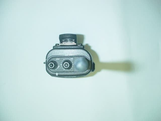
PM3GT40
Dec 08, 2004UHF LMRS TRANSMITTER
Equipment Class
TNF - Licensed Non-Broadcast Transmitter Held to Face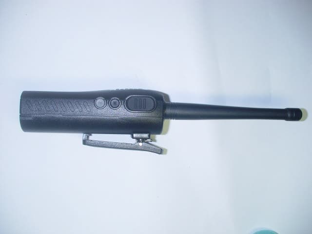
PM3GT10
Dec 08, 2004UHF LMRS TRANSMITTER
Equipment Class
TNF - Licensed Non-Broadcast Transmitter Held to Face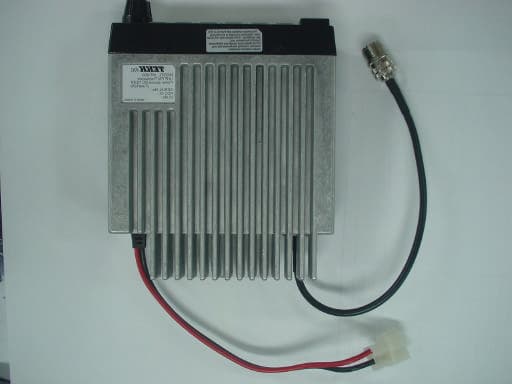
PM3MT900
Nov 28, 2004LAND MOBILE RADIO SERVICE GMRS TRANSMITTER
Equipment Class
TNB - Licensed Non-Broadcast Station Transmitter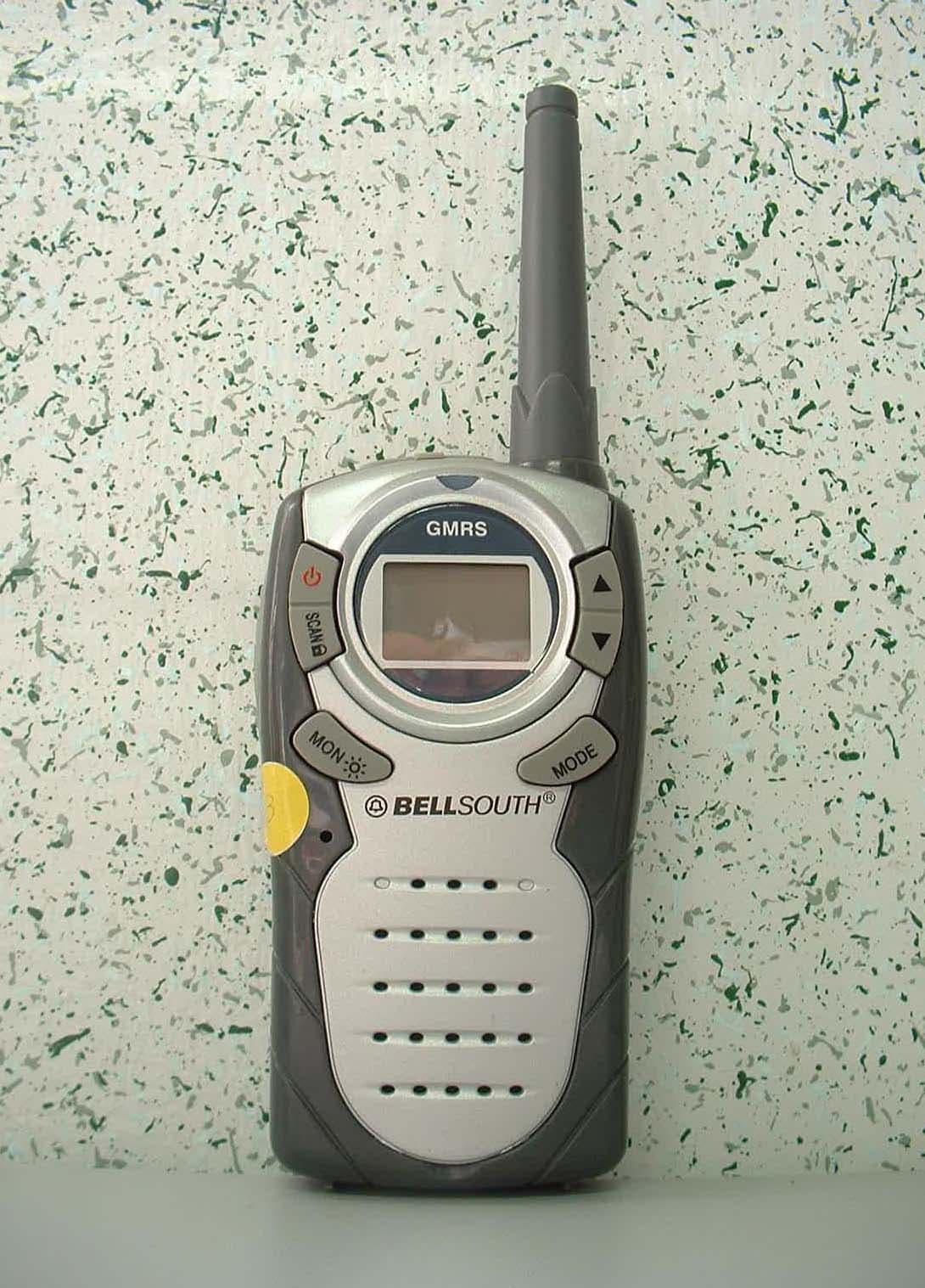
PM3GR5500
Jul 18, 2004GMRS/FRS UHF Transceiver
Equipment Class
FRF - Part 95 Family Radio Face Held Transmitter
PM3GX80
Jul 01, 2004Transceiver, VHF, PTT
Equipment Class
TNF - Licensed Non-Broadcast Transmitter Held to Face