PYN12002ALicensed Transmitter
ComSonics, Inc.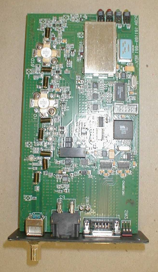
Click to zoom
Application Details
- Equipment Class
- TNB - Licensed Non-Broadcast Station Transmitter
- Date of Grant
- Aug 11, 2002
- Application Purpose
- Original Equipment
- Date of Application
- Apr 18, 2002
- Equipment Note
- Licensed Transmitter
- Frequency Range
- 27.45000000 - 27.49000000
- Company
- ComSonics, Inc.
- Country
- United States
Documents & Files
Document Text
Text extracted from the exhibit documents filed with the FCC. Open a document above to read the original.
Users Manual
Ingression Measurement Transmitter Operating Instructions Included in the package you will find: 1) One Ingression Measurement Transmitter, suitable for documentation purposes. 2) Two Ingression Measurement Transmitters - modified, suitable for F.C.C. Certification Testing. 3) One power cable, for applying DC power to the unit 4) One cable with DB-9 connectors on each end. * 5) All documentation required per the "checklist" issued by Washington Labs. Additional items required to operate the transmitter include: 1) a personal computer with a serial port running the Disk Operating System (DOS) 2) a regulated DC power supply of 13.8 volts capable of supplying 20 amperes 3) 50 ohm load for the antenna, capable of dissipating 20 watts Plug the DC power cable into the "POWER" jack on the rear panel of the IMT. Plug the DB-9 connector into the DB-9 receptacle on the rear panel of the IMT. Connect a suitable load (resistive, 50 ohm) to the "ANTENNA" connector on the rear panel of the IMT. DO NOT OPERATE THIS TRANSMITTER WITHOUT A PROPER 50 OHM LOAD! After making sure the power supply is in the "off" state, connect the free end of the power cable to the DC power supply. Red wire is positive and black wire is negative. Connect the other end of the DB-9 cable to the test computer Flip the power switch on the power supply to the "ON" state. Flip the power switch on the front panel of the IMT to the "ON" state. Copy the test program "IMT-TEST.EXE" from the cdrom to your test computer. The main screen of the test program will display all instructions necessary to proceed with setting frequency and transmit control. It is possible that, during the testing cycle, the IMT will overheat. There is a built-in temperature sensor that prevents transmitter operation when this condition occurs. There is an LED on the front panel that will illuminate indicating this condition. This transmitter was designed with a 1:9 duty cycle, specifically 100mS on and 900mS off. The modified test units have larger wattage collector resistors, giving the ability to transmit for longer periods of time. Do not transmit for more than 5 to 6 seconds at a time. Damage to these resistors will occur. There is a 3 pin header located near U5. Placing the jumper on one side of the header will enable the FM deviation and placing it on the other side of the header will disable the FM deviation. * You must use the cable provided. The connector on the rear panel of the IMT is not standard.
Cover Letter(s)
February 4, 2002 Chief, Authorizations Branch Federal Communications Commission 7435 Oakland Mills Road Columbia, MD 21046 To Whom It May Concern: Please be advised that ComSonics, Inc. authorizes Washington Laboratories, Ltd. to act on our behalf, until otherwise notified, for applications submitted to the Federal Communications Commission (FCC). We certify that we are not subject to denial of federal benefits, that includes FCC benefits, pursuant to Section 5301 of the Anti-Drug Abuse Act of 1988, U.S.C. 862. Further, no party, as defined in 47 CFR 1.2002(b), to the application is subject to denial of federal benefits, that includes FCC benefits. Thank you for your attention to this matter. Dick Shimp Chief of New Technology ComSonics, Inc.
Internal Photos
Overall View, Disassembled PCB Top PCB Top, Shield Removed PCB Bottom
Operational Description
Qualifier Transmitter Theory of Operation Please refer to the Qualifier Block Diagram (imt-block.pdf) and Qualifier Schematics (imt-sch1.pdf through imt-sch8.pdf) R.F. Generation and Amplification - Signal Path Description RF energy is produced by a voltage controlled oscillator circuit at Q8. Correction voltage is supplied by PLL at U4 for tuning the tank circuit varactor. The PLL reference signal is produced by VCXO1, a voltage controlled crystal oscillator operating at 15.36 MHz. The PLL is programmed to provide one of three frequencies by the microcontroller at U11. 27.45 MHz, 27.47 MHz, and 27.49 MHz, therefore providing a channel spacing of 20KHz. The RF energy from oscillator Q8 is amplified by buffer stage Q21. There is a ’PI’ type attenuator pad providing -10dB of gain, used to limit the amount of RF energy between the VCO buffer at Q21 and the next gain stage in the series at A1. A1 is a MMIC providing about +20dB of gain. From there, the RF energy is passed through a variable attenuator, comprised of PIN diodes D8 and D9. This variable attenuator provides -1dB to -55dB of gain, giving ample control range over the output signal. The RF energy is then passed into the driver stage at Q20, which provides a +13dB gain. The final stage in the chain at Q1 provides +13dB worth of gain. The RF signal is then low pass filtered and finally band pass filtered before connecting to the external antenna connector. The band pass filter serves another purpose, that is to provide a high impedence at the antenna connector at 433 MHz, the frequency at which the ASH receiver at IC9 operates. R.F. Power Control The RF energy is sampled near the antenna connector by an AD8307 at U9. This device produces a voltage output that is proportional to the RF input signal level. The voltage output is gain and D.C. offset corrected by an op-amp at U10A. It is then compared to a reference voltage by an op-amp at U15A. The reference voltage is produced by a resistor network, controlled by the microcontroller through a 1 of 8 decoder at U16. The output from this comparison at U15A is fed into the variable PIN diode attenuator at D8 and D9, providing a gain control range of -1dB to -55dB. GMSK Signal Generation and Two Point Modulation System The GMSK signal is produced by an MX-589 at U5. This signal is filtered by an op-amp network comprised of U6B, U6A, U8B, U8A, U7A, and U7B. The signal path splits at U7A and U7B, with the output from U7A going to the VXCO at VXCO1, providing a reference offset for the PLL and the output from U7B going to the varactor diode in the oscillator’s tank circuit at D5. By applying the modulating signal to both the oscillator and the PLL reference source simultaneously, you minimize the distorting characteristics caused by the PLL’s normal operation. The modulating frequency range runs from D.C. through 7.2 KHz, deviating the output frequency by 15 KHz. Temperature Sensor - Thermal Shutdown The sensor at IC6 is used to monitor the temperature of the final amplifier. The voltage from the sensor is compared to a reference voltage by an op-amp at IC5B. When the temperature sensor’s voltage exceeds that of the reference voltage, an input pin on the microcontroller is pulled low. The controlling software will monitor this pin every 10mS and when an over temperature condition is met, the microcontroller software will prevent the unit from further transmissions. There is an LED on the front panel that will notify a user of this condition. VSWR Sensor There is a VSWR monitoring circuit, comprised of detectors DX1, and DX2, and an op-amp at IC5A. When this detector circuit detects a VSWR level that is above a preset level, the op-amp will pull a pin on the microcontroller low. The controlling software will then prevent any further transmissions until the power is cycled OFF and back ON. This is intended to prevent the use of the transmitter with an improperly matched antenna. There is an LED on the front panel that will notify a user of this condition. NOTE: The units sent to your facility for testing will not require a power off-on sequence to reset from a mismatch at the antenna connector. PLL Lock Monitoring The microcontroller monitors the state of the PLL device and will prevent transmissions when an "out of lock" condition is detected. ASH Receiver (Command Link) There is an ASH receiver at IC9 tuned to 433.92 MHz. This receiver is used for data reception from the Qualifier hand held unit. The data output from this device is delivered to both the main microcontroller at U11 and to an additional microcontroller at U1000. The device at U1000 is used to detect a start of transmission sequence from the data stream and notify the microcontroller at U11 of this. The main microcontroller at U11 will then parse the data stream and extract the control message from it. This data stream is used to control the operating characteristics of the IMT unit, such as when to transmit, what power level to use, how many transmissions, the frequency to use, etc. Output Frequency Selection The operating frequency is controlled by the microcontroller at U11 with inputs either from the command link data stream or from an external computer. The frequency selection is one of three possible frequencies, 27.45 MHz, 27.47 MHz, or 27.49 MHz. Safety Shutdown In case of microcontroller failure, the unit will cease transmitting within 240 mS. There is an R-C circuit in the transmitter’s control line that will shut power off to the driver and final amplifier stages. NOTE: This feature has been disabled in the two units your facility has for testing. Modes of Operation The transmitter will operate in one of two modes. Mode one is an on/off cycling of the transmission signal with a low duty cycle. The transmitter will be ON for 100mS then OFF for 900mS, repeating. Mode two, the transmitter will transmit three short bursts, followed by a period of inactivity, then may transmit this three burst pattern again, up to two addi…
Text truncated - open the document above for the full version.
Parts List/Tune Up Info
Qualifier Transmitter Bill of Materials1 1 101110-001 PCB TRANSMITTER QUALIFIER 1 EA P1 2 101109 ASSY DWG PCBA TRANSMITTER QUALIFIER A/R EA S Y1 3 S101109 SCHEMATIC PCBA TRANSMITTER QUALIFIER A/R EA S Y1 4 T101109 TP PCBA TRANSMITTER QUALIFIER A/R EA S Y1 10 EC-645 CAP SM 47UF 10V REEL 2 EA P C6, C481 11 EC-686 CAP SM TANT 1UF 16V (REEL) 14 EA P C63, C89, C90, C92, C94, C95, C96, C97, C98, C121, C122, C134, C135, CX211 12 EC-875 CAP TANT 10UF 16V A-PKG SM (REEL) 3 EA P C88, C129, C1301 13 EC-661 CAP SM 33UF 16V TANT REEL 2 EA P C2, C31 15 EC-654 CAP SM 0.001UF NPO 50V REEL 7 EA P C11, C13, C43, C53, C82, C102, C1081 16 EC-642 CAP SM 0.01UF X7R 50V 0805 (REEL) 6 EA P C12, C51, C56, C71, C85, C1071 17 EC-778 CAP SM .033UF X7R 50V 5% 0805 REEL 2 EA P C66, C671 18 EC-804 CAP SM .1UF X7R 50V 5% 0805 (REEL) 17 EA P C1, C4, C7, C40, C49, C84, C100, C103, C104, C106, C109, C114, C124, C126, C127, C133, CX161 19 EC-679 CAP SM 100PF 50V NPO 0805 REEL 2 EA P C83, C861 20 EC-650 CAP SM 10PF NPO 50V 0805 REEL 2 EA P C112, CX21 21 EC-656 CAP SM 18PF COG 50V 0805 REEL 5 EA P C70, C73, C74, C91, C931 23 EC-676 CAP SM 330PF 50V NPO 0805 1 EA P C381 24 EC-729 CAP SM 390PF 50V NPO 0805 REEL 1 EA P C681 25 EC-730 CAP SM 470PF 50V NPO 0805 REEL 3 EA P C58, C64, C721 26 EC-740 CAP SM 68PF 0805 NPO 50V REEL 2 EA P C28, C1111 27 EC-646 CAP SM 0.1UF X7R 50V 1206 REEL 8 EA P C8, C46, C55, C57, C99, C110, CX5, CX91 28 EC-665 CAP SM 0.33UF 50V 1206 REEL 1 EA P C451 29 EC-833 CAP SM 270PF NPO 50V 5% 1206 (REEL) 1 EA P C27, C301 30 EC-652 CAP SM 2.2UF 20V 1 EA P CX111 31 EC-657 CAP SM 12PF NPO 50V 0805 REEL 2 EA P CX23, CX251 32 EC-879 CAP SM TRIMMER 6-35PF 5 EA P C116, C117, C118, C119, CX2A1 33 EC-715 CAP SM 39PF NPO 50V 5% 0805 1 EA P C651 34 EC-716 CAP SM 0.01 X7R 50V 10% 0603 REEL 10 EA P C16A, C39, C59A, CX1, CX6, CX7, CX8, CX12, CX17, CX261 35 EC-724 CAP TANT 10UF 6.3V B-PKG SM 1 EA P CX141 36 EC-734 CAP SM 5.6PF 50V NPO 0805 1 EA P CX241 37 EC-752 CAP SM 100PF NPO 50V 0603 REEL 4 EA P CX2B, CX13, CX15, CX221 38 EC-757 CAP SM 0.1UF Y5V 25V 0603 REEL 5 EA P C101, C125, C132, CX3, CX41 39 EC-761 CAP SM 390PF NPO 50V 0603 REEL 1 EA P C691 40 EC-811 CAP SM TANT 2.2UF 20V SIZE A (REEL) 1 EA P C91 41 EC-838 CAP SM 12PF NPO 200V 10% 1206 (REEL) 3 EA P C76, CX18, CX201 42 EC-822 CAP SM 150PF NPO 200V 10% 1206 (REEL) 2 EA P C25, C801 43 EC-823 CAP SM 220PF NPO 200V 10% 1206 (REEL) 3 EA P C18, C23, C1131 44 EC-818 CAP SM 33PF NPO 200V 10% 1206 (REEL) 1 EA P C1151 45 EC-819 CAP SM 47PF NPO 200V 10% 1206 (REEL) 1 EA P C811 46 EC-821 CAP SM 68PF NPO 200V 10% 1206 (REEL) 1 EA P C791 47 EC-841 CAP SM 1UF X7R 25V 10% 1206 (REEL) 6 EA P C41, C50, C54, C120, C140, C5601 49 EC-867 CAP SM 0.22UF X7R 16V 0805 (REEL) 1 EA P C521 50 EC-869 CAP SM 15PF NPO 50V 1206 (REEL) 1 EA P C1281 51 EC-870 CAP SM 300PF NPO 200V 0805 (REEL) 1 EA P C151 52 EC-868 CAP SM 330PF NPO 50V 1206 (REEL) 1 EA P C321 53 EC-872 CAP SM 5.6PF NPO 50V 0805 (REEL) 1 EA P CX191 54 EC-873 CAP SM 5600PF X7R 50V 0603 (REEL) 1 EA P C601 55 EC-874 CAP SM 5600PF X7R 50V 0805 (REEL) 3 EA P C59, C61, C621 56 EC-871 CAP SM 91PF NPO 50V 1206 (REEL) 1 EA P C21 1 60 RW-853 RES SM 1/10W 5% 22 0805 REEL 1 EA P R441 61 RX-531 RES SM 1/10W 5% 39 0805 (REEL) 1 EA P R161 62 RW-849 RES SM 1/10W 5% 51 0805 REEL 2 EA P R97, R1001 63 RW-882 RES SM 1/10W 5% 82 0805 REEL 1 EA P R841 64 RW-841 RES SM 1/10W 5% 200 0805 REEL 1 EA P R101 65 RW-863 RES SM 1/10W 5% 300 2 EA P R96, R1011 66 RW-876 RES SM 1/10W 5% 330 0805 REEL 1 EA P R591 67 RW-869 RES SM 1/10W 5% 390 2 EA P R25, R1191 68 RW-875 RES SM 1/10W 5% 430 0805 REEL 6 EA P R22, R54, R55, R56, R56A, R56B1 69 RW-767 RES SM 1/10W 5% 470 (REEL) 5 EA P R109, R110, R113, R114, R1151 70 RW-999 RES SM 1/10W 5% 560 0805 (REEL) 2 EA P R60, R611 71 RW-889 RES SM 1/10W 5% 1.6K 0805 2 EA P R63, R641 72 RW-819 RES SM 1/10W 5% 100K 0805 REEL 2 EA P R42, R431 73 RX-790 RES SM 1/16W 5% 5.6K 0603 (REEL) 1 EA P R1A1 74 RW-898 RES SM 1/10W 5% 10M 1 EA P R371 75 RX-559 RES SM 1/10W 5% 220K 0805 (REEL) 3 EA P R34, R36, R391 76 RW-850 RES SM 1/10W 5% 22K 0805 REEL 1 EA P R711 77 RW-862 RES SM 1/10W 5% 3.3K 0805 REEL 3 EA P R13, R23, R851 78 RX-569 RES SM 1/16W 5% 1K 0603 REEL 1 EA P R59A1 79 RW-768 RES SM 1/10W 5% 33K 1 EA P R181 80 RW-859 RES SM 1/10W 5% 39K 0805 REEL 3 EA P R27, R90, R911 81 RW-845 RES SM 1/10W 5% 47K 0805 REEL 5 EA P R24, R31, R35, R65, R671 82 RW-825 RES SM 1/10W 5% 5.1K 0805 REEL 2 EA P R76, R1201 83 RW-979 RES SM 1/10W 5% 6.2K 0805 REEL 2 EA P R82, R831 84 RW-824 RES SM 1/10W 5% 1.8K 0805 REEL 1 EA P R211 85 RW-857 RES SM 1/10W 1% 1K 0805 REEL 1 EA P R69, R751 86 RW-873 RES SM 1/10W 5% 100 0805 REEL 2 EA P R121, R1221 87 RW-880 RES SM 0 JUMPER 0805 (REEL) 4 EA P C123, R29, R38, R1041 88 RW-881 RES SM 1/10W 5% 1.2K 0805 REEL 1 EA P R1231 89 RW-899 RES SM 1/10W 1% 11K 0805 2 EA P R74, R771 90 RW-903 RES SM 1/10W 1% 10K 0805 REEL 5 EA P R92, R93, R94, R95, R1061 91 RW-909 RES SM 1/10W 5% 2K 0805 REEL 2 EA P R50, R1021 92 RW-947 RES SM 1/10W 5% 56 0805 REEL 1 EA P R1241 93 RW-953 RES SM 1/10W 1% 20.0K 2 EA P R88, R891 94 RW-954 RES SM 1/10W 1% 33.2K 1 EA P R531 95 RW-995 RES SM 1/10W 1% 100K 0805 REEL 1 EA P R171 96 RX-501 RES SM 1/10W 5% 51K 0805 REEL 1 EA P R471 97 RX-532 RES SM 1/10W 5% 2.7K 0805 (REEL) 2 EA P R116, R1171 98 RX-541 RES SM 1/16W 5% 100 0603 REEL 1 EA P RX171 99 RX-542 RES SM 1/16W 5% 10 0603 REEL 3 EA P RX6, RX7A, RX141 100 QIC-918 IC SM GMSK ENCODER/DECODER TUBE 1 EA P U51 101 QIC-729 IC HEX INVERTER SM TUBE 2 EA P IC4, U21 103 QIC-921 IC MICROPROC 8051COMP 12K FLASH (TUBE) 1 EA P U11- bake as needed prior to assembly.1 104 QIC-924 IC FREQ SYNTH 1.1GHz DUAL MOD (TUBE) 1 EA P U41 105 QIC-923 IC SM VOLTAGE REG +5 AUTOMOTIVE (TUBE) 2 EA P U1, U31 106 QIC-990 IC DUAL RS232 TX/RX SM TUBE 2 EA P U12, U141 107 QIC-976 IC AMPLIFIER LOGARITHMIC 1 EA P U91 108 QIC-886 IC RF AMP DC-8GHz SM 1 EA P A11 109 QIC-837 IC NPROCESSOR RESET SO223 SM (REEL) 1 EA P U13 1 110 QIC-930 TRANSISTOR FLANGED NPN RF POWER 2 EA P Q1, Q201 112 QIC-65…
Text truncated - open the document above for the full version.
Test Report
Document 6880-01, Rev. 0 FCC ID: PYN12002A FCC Certification Test Report Washington Laboratories, Ltd April 2002 FCC Certification Test Report for ComSonics, Inc. PYN12002A April 18, 2002 - Prepared for: ComSonics, Inc. 1350 Port Republic Road Harrisonburg, VA 22801 Prepared By: Washington Laboratories, Ltd. 7560 Lindbergh Drive Gaithersburg, Maryland 20879 FCC Certification Test Report Document 6880-01, Rev. 0 FCC ID: PYN12002A FCC Certification Test Report Washington Laboratories, Ltd April 2002 FCC Certification Test Program FCC Certification Test Report for the ComSonics, Inc. 27 MHz Ingression Measurement Transmitter PYN12002A April 18, 2002 WLL JOB# 6880 Prepared by: Brian J. Dettling Documentation Specialist Reviewed by: Michael F. Violette President Document 6880-01, Rev. 0 FCC ID: PYN12002A FCC Certification Test Report Washington Laboratories, Ltd April 2002 ii Abstract This report has been prepared on behalf of ComSonics, Inc. to support the attached Application for Equipment Authorization. The test report and application are submitted for a Licensed Transmitter under Part 90.35 of the FCC Rules and Regulations. This Federal Communication Commission (FCC) Certification Test Report documents the test configuration and test results for a ComSonics, Inc. 27 MHz Ingression Measurement Transmitter. Testing was performed on an Open Area Test Site (OATS) of Washington Laboratories, Ltd, 7560 Lindbergh Drive, Gaithersburg, MD 20879. Site description and site attenuation data have been placed on file with the FCC's Sampling and Measurements Branch at the FCC laboratory in Columbia, MD. Washington Laboratories, Ltd. has been accepted by the FCC and approved by NIST NVLAP (NVLAP Lab Code: 200066-0) as an independent FCC test laboratory. The ComSonics, Inc. 27 MHz Ingression Measurement Transmitter complies with the limits for a Licensed Transmitter device under Part 90.35 of the FCC Rules and Regulations. Document 6880-01, Rev. 0 FCC ID: PYN12002A FCC Certification Test Report Washington Laboratories, Ltd April 2002 iii Table of Contents Abstract......................................................................................................ii 1 Introduction...................................................................................................................1 1.1 Compliance Statement..........................................................................................1 1.2 Test Scope..........................................................................................................1 1.3 Contract Information............................................................................................1 1.4 Test Dates...........................................................................................................1 1.5 Test and Support Personnel..................................................................................1 1.6 Abbreviations.......................................................................................................2 2 Equipment Under Test....................................................................................................3 2.1 EUT Identification & Description..........................................................................3 2.2 Test Configuration................................................................................................3 2.3 Testing Algorithm.................................................................................................3 2.4 Test Location.......................................................................................................4 2.5 Measurements......................................................................................................4 2.5.1 References...................................................................................................4 2.6 Measurement Uncertainty.....................................................................................4 3 Test Equipment..............................................................................................................4 4 Test Results...................................................................................................................5 4.1 Duty Cycle Correction.........................................Error! Bookmark not defined. 4.2 RF Power Output: (FCC Part §2.1046)...............................................................5 4.3 Modulation Characteristics: (FCC Part §2.1047); Audio Frequency Response......6 4.4 Occupied Bandwidth: (FCC Part §2.1049)..........................................................6 4.5 Spurious Emissions at Antenna Terminals (FCC Part §2.1051...............................8 4.6 Radiated Spurious Emissions: (FCC Part §2.1053).............................................13 4.6.1 Test Procedure........................................................................................13 4.7 Frequency Stability: (FCC Part §2.1055)...........................................................15 4.8 Transient Frequency Response (Part 90.214).....................................................16 5 Transmitter Environmental Assessment, Maximum Permissible Exposure (MPE)............17 5.1 SCOPE.............................................................................................................17 5.2 REFERENCE....................................................................................................17 Document 6880-01, Rev. 0 FCC ID: PYN12002A FCC Certification Test Report Washington Laboratories, Ltd April 2002 iv List of Tables Table 1. Device Summary....................................................................................................3 Table 2: Test Equipment List...............................................................................................5 Table 3. Duty Cycle Correction............................................Error! Bookmark not defined. Table 4. RF Power Output.............................…
Text truncated - open the document above for the full version.
Test Report
Document 6880-01, Rev. 1 FCC ID: PYN12002A FCC Certification Test Report Washington Laboratories, Ltd April 2002 FCC Certification Test Report for ComSonics, Inc. PYN12002A Revision 1 July 18, 2002 - Prepared for: ComSonics, Inc. 1350 Port Republic Road Harrisonburg, VA 22801 Prepared By: Washington Laboratories, Ltd. 7560 Lindbergh Drive Gaithersburg, Maryland 20879 FCC Certification Test Report Document 6880-01, Rev. 1 FCC ID: PYN12002A FCC Certification Test Report Washington Laboratories, Ltd April 2002 FCC Certification Test Program FCC Certification Test Report for the ComSonics, Inc. 27 MHz Ingression Measurement Transmitter PYN12002A Revision 1 July 18, 2002 WLL JOB# 6880 Prepared by: Brian J. Dettling Documentation Specialist Reviewed by: Michael F. Violette President Document 6880-01, Rev. 1 FCC ID: PYN12002A FCC Certification Test Report Washington Laboratories, Ltd April 2002 ii Abstract This report has been prepared on behalf of ComSonics, Inc. to support the attached Application for Equipment Authorization. The test report and application are submitted for a Licensed Transmitter under Part 90.35 of the FCC Rules and Regulations. This Federal Communication Commission (FCC) Certification Test Report documents the test configuration and test results for a ComSonics, Inc. 27 MHz Ingression Measurement Transmitter. Testing was performed on an Open Area Test Site (OATS) of Washington Laboratories, Ltd, 7560 Lindbergh Drive, Gaithersburg, MD 20879. Site description and site attenuation data have been placed on file with the FCC's Sampling and Measurements Branch at the FCC laboratory in Columbia, MD. Washington Laboratories, Ltd. has been accepted by the FCC and approved by NIST NVLAP (NVLAP Lab Code: 200066-0) as an independent FCC test laboratory. The ComSonics, Inc. 27 MHz Ingression Measurement Transmitter complies with the limits for a Licensed Transmitter device under Part 90.35 of the FCC Rules and Regulations. Document 6880-01, Rev. 1 FCC ID: PYN12002A FCC Certification Test Report Washington Laboratories, Ltd April 2002 iii Table of Contents Abstract......................................................................................................ii 1 Introduction...................................................................................................................1 1.1 Compliance Statement..........................................................................................1 1.2 Test Scope..........................................................................................................1 1.3 Contract Information............................................................................................1 1.4 Test Dates...........................................................................................................1 1.5 Test and Support Personnel..................................................................................1 1.6 Abbreviations.......................................................................................................2 2 Equipment Under Test....................................................................................................3 2.1 EUT Identification & Description..........................................................................3 2.2 Test Configuration................................................................................................3 2.3 Testing Algorithm.................................................................................................3 2.4 Test Location.......................................................................................................4 2.5 Measurements......................................................................................................4 2.5.1 References...................................................................................................4 2.6 Measurement Uncertainty.....................................................................................4 3 Test Equipment..............................................................................................................5 4 Test Results...................................................................................................................6 4.1 Emission Designation Calculation..........................................................................6 4.2 RF Power Output: (FCC Part §2.1046)...............................................................6 4.3 Modulation Characteristics: (FCC Part §2.1047); Audio Frequency Response......6 4.4 Occupied Bandwidth: (FCC Part §2.1049)..........................................................7 4.5 Spurious Emissions at Antenna Terminals (FCC Part §2.1051...............................9 4.6 Radiated Spurious Emissions: (FCC Part §2.1053).............................................14 4.6.1 Test Procedure........................................................................................14 4.7 Frequency Stability: (FCC Part §2.1055)...........................................................16 4.8 Transient Frequency Response (Part 90.214).....................................................17 5 Transmitter Environmental Assessment, Maximum Permissible Exposure (MPE)............18 5.1 SCOPE.............................................................................................................18 5.2 REFERENCE....................................................................................................18 Document 6880-01, Rev. 1 FCC ID: PYN12002A FCC Certification Test Report Washington Laboratories, Ltd April 2002 iv List of Figures Figure 1. Device Summary...................................................................................................3 Figure 2: Test Equipment List..............................................................................................5 Figure 3. RF Power Output.............................................................................................…
Text truncated - open the document above for the full version.
Test Setup Photos
Radiated Emissions Test Setup
Contact Information
Applicant
Richard L Shimp(Chief of Technology)
Technical Contact
Washington Laboratories, Ltd.Gregory M Snyder
[email protected]301/ 417-0220
7560 Lindbergh Drive · Gaithersburg, Maryland · United States
Non-Technical Contact
Washington Laboratories, Ltd.Brian J Dettling
[email protected]301/ 417-0220
Test Firm
Washington Laboratories, Ltd.Michael Violette
Technical Specifications
| # | Rule Parts | Frequency Range | Power Output | Emission | Tolerance |
|---|---|---|---|---|---|
| 1 | 90 | 27.45 MHz - 27.49 MHz | 20 W | 50K4G1D | 0.0020000000 ppm |
Other Applications from ComSonics, Inc.
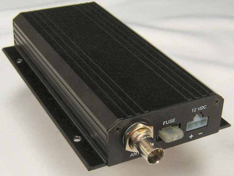
PYN2007VMD
Mar 20, 2008Vehicle Mounted Transmitter
Equipment Class
TNB - Licensed Non-Broadcast Station Transmitter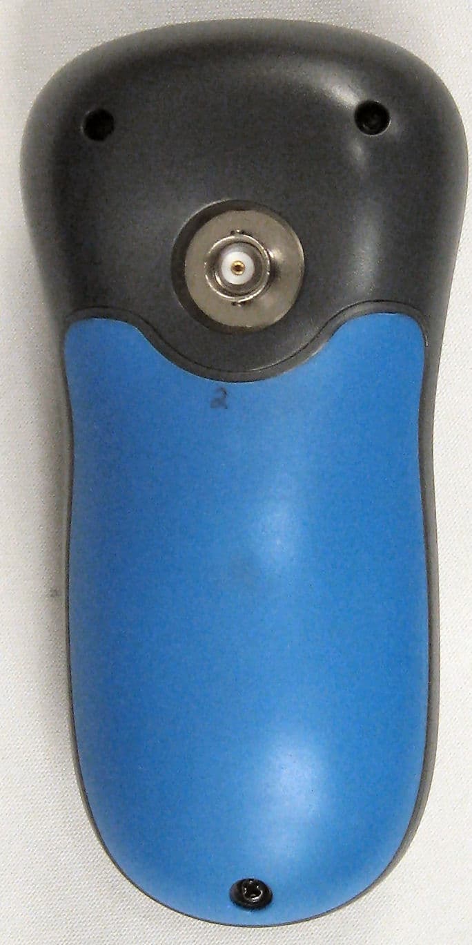
PYN2007HHD
Sep 09, 2007Remote Control Device
Equipment Class
DSC - Part 15 Security/Remote Control Transmitter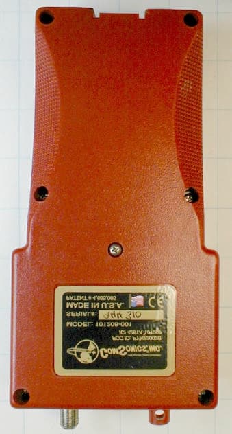
PYN22002B
Dec 09, 2002Home Qualification System
Equipment Class
DSC - Part 15 Security/Remote Control Transmitter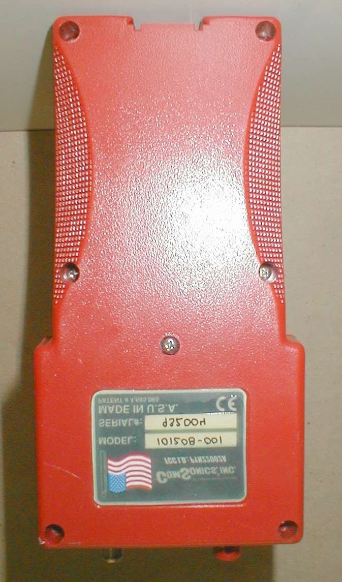
PYN22002A
Mar 26, 2002Wireless Remote
Equipment Class
DSC - Part 15 Security/Remote Control Transmitter