QIPPHS8-PGSM/GPRS/UMTS/HSPA Module
Telit Cinterion Deutschland GmbH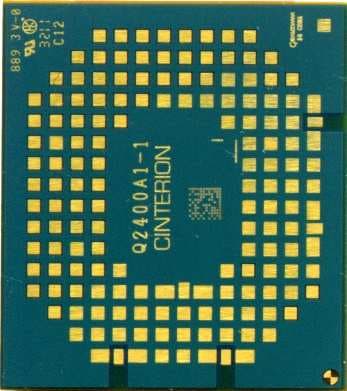
Click to zoom
Application Details
- Equipment Class
- JBP - Part 15 Class B Computing Device Peripheral
- Date of Grant
- Dec 06, 2011
- Application Purpose
- Original Equipment
- Date of Application
- Dec 06, 2011
- Equipment Note
- GSM/GPRS/UMTS/HSPA Module
- Country
- Germany
Documents & Files
Document Text
Text extracted from the exhibit documents filed with the FCC. Open a document above to read the original.
Users Manual
PHS8-P Version:01.000 DocId:PHS8-P_HIO_v01.000 Hardware Interface Overview GENERAL NOTE THE USE OF THE PRODUCT INCLUDING THE SOFTWARE AND DOCUMENTATION (THE "PROD- UCT") IS SUBJECT TO THE RELEASE NOTE PROVIDED TOGETHER WITH PRODUCT. IN ANY EVENT THE PROVISIONS OF THE RELEASE NOTE SHALL PREVAIL. THIS DOCUMENT CON- TAINS INFORMATION ON CINTERION PRODUCTS. THE SPECIFICATIONS IN THIS DOCUMENT ARE SUBJECT TO CHANGE AT CINTERION'S DISCRETION. CINTERION WIRELESS MODULES GMBH GRANTS A NON-EXCLUSIVE RIGHT TO USE THE PRODUCT. THE RECIPIENT SHALL NOT TRANSFER, COPY, MODIFY, TRANSLATE, REVERSE ENGINEER, CREATE DERIVATIVE WORKS; DISASSEMBLE OR DECOMPILE THE PRODUCT OR OTHERWISE USE THE PRODUCT EXCEPT AS SPECIFICALLY AUTHORIZED. THE PRODUCT AND THIS DOCUMENT ARE PROVIDED ON AN "AS IS" BASIS ONLY AND MAY CONTAIN DEFICIENCIES OR INADEQUACIES. TO THE MAXIMUM EXTENT PERMITTED BY APPLICABLE LAW, CINTERION WIRELESS MODULES GMBH DIS- CLAIMS ALL WARRANTIES AND LIABILITIES. THE RECIPIENT UNDERTAKES FOR AN UNLIMITED PERIOD OF TIME TO OBSERVE SECRECY REGARDING ANY INFORMATION AND DATA PRO- VIDED TO HIM IN THE CONTEXT OF THE DELIVERY OF THE PRODUCT. THIS GENERAL NOTE SHALL BE GOVERNED AND CONSTRUED ACCORDING TO GERMAN LAW. Copyright Transmittal, reproduction, dissemination and/or editing of this document as well as utilization of its con- tents and communication thereof to others without express authorization are prohibited. Offenders will be held liable for payment of damages. All rights created by patent grant or registration of a utility model or design patent are reserved. Copyright © 2011, Cinterion Wireless Modules GmbH Trademark Notice Microsoft and Windows are either registered trademarks or trademarks of Microsoft Corporation in the United States and/or other countries. All other registered trademarks or trademarks mentioned in this document are property of their respective owners. PHS8-P_HIO_v01.000Page 2 of 412011-11-10 Confidential / Released PHS8-P Hardware Interface Overview 2 Document Name: PHS8-P Hardware Interface Overview Version: 01.000 Date: 2011-11-10 DocId: PHS8-P_HIO_v01.000 Status Confidential / Released PHS8-P Hardware Interface Overview Contents 41 PHS8-P_HIO_v01.000Page 3 of 412011-11-10 Confidential / Released Contents 1Introduction ................................................................................................................. 6 1.1Related Documents ........................................................................................... 6 1.2Terms and Abbreviations ................................................................................... 6 1.3Regulatory and Type Approval Information ..................................................... 10 1.3.1Directives and Standards .................................................................... 10 1.3.2SAR requirements specific to portable mobiles .................................. 13 1.3.3SELV Requirements ........................................................................... 14 1.3.4Safety Precautions .............................................................................. 14 2Product Concept ....................................................................................................... 16 2.1Key Features at a Glance ................................................................................ 16 2.2PHS8-P System Overview ............................................................................... 19 3Application Interface................................................................................................. 20 3.1Operating Modes ............................................................................................. 21 3.2Power Supply ................................................................................................... 22 3.3USB Interface................................................................................................... 23 3.4Serial Interface ASC0 ...................................................................................... 24 3.5UICC/SIM/USIM Interface ................................................................................ 26 3.6Analog Audio Interface..................................................................................... 28 3.7Digital Audio Interface ...................................................................................... 28 4GPS Receiver............................................................................................................. 29 5Antenna Interfaces.................................................................................................... 30 5.1GSM/UMTS Antenna Interface ........................................................................ 30 5.1.1Antenna Installation ............................................................................ 31 5.2GPS Antenna Interface .................................................................................... 32 6Mechanics.................................................................................................................. 34 6.1Mechanical Dimensions of PHS8-P ................................................................. 34 7Sample Application................................................................................................... 36 8Reference Approval .................................................................................................. 38 8.1Reference Equipment for Type Approval ......................................................... 38 8.2Compliance with FCC and IC Rules and Regulations ..................................... 39 9Appendix.................................................................................................................... 40 9.1List of Parts and Accessories........................................................................... 40 PHS8-P Hardware Interface Overview Ta b l e s 41 PHS8-P_HIO_v01.000Page 4 of 412011-11-10 Confidential / Releas…
Text truncated - open the document above for the full version.
Cover Letter(s)
r---------~~ Cintenon Wireless Modules GmbH· Siemensdamm 50 • 13629 Benin· Germany Federal Communication Commission Name Thorsten Liebig Equipment Authorization Division, Application Department Manager Approval Processing Branch 7435 Oakland Mills Road Phone +49 30 31102-8241 Columbia, MD 21048 Fax +493031102-8305 E-Mail [email protected] Your letter of Our reference Date 23 November 2011 Request for Sbort Term Confidentiality FCC ID: QIPPHS8-P To Whom It May Concern: In accordance with §0.459(d) of CFR 47 and Public Notice DA 04-1705, Cinterion requests The following item 1. User Guide / Installation Manual 2. Internal Photographs be held short term confidential until 31 sI of December 2011 These items contain detailed system and equipment description and related information about the product which Cinterion considers to be proprietary, confidential and a custom design which otherwise would not be released to the general public. Since this design is a basis from which future technological products will evolve, Cinterion also feels that this information would be of benefit to its competitors, and that the disclosure of the information in these exhibits would give our competitors an unfair advantage in the market. Sincerely Thorsten Liebig Manager Approval Registered office: Managing directors: Commercial register, Reg. no.: Cintenon Wireless Modules GmbH Norbert Muhrer. Sebastien Gallois Amtsgericht München, HRB 172715 St.-Martin-Straße 53 WEEE-Reg.-Nr. DE 58893809 81669 München Genmany
Cover Letter(s)
--;;;;; Cintarion Wireless Modules GmbH· Siemensdamm 5.0 • 13629 Bertin • Germany Name Thorsten Liebig Federal Communication Commission Department Manager Approval Equipment Authorization Division, Application Processing Branch 7435 Oakland Mills Road Phone +493031102-8241 Fax +493031102-8305 Columbia, MD 21048 E-Mail [email protected] Your letter of Our reference Date 23 November 2011 TO WHOM IT MA Y CONCERN Pursuant to Paragraphs §0.457 and 0.459 of the Commission's Rules (47 C.F.R.) and Section §552(b)(4) of the Freedom of Information Act, Cinterion requests confidentiality for the following products: FCC ID Number Product Title/Model QIPPHS8-P Cinterion Wireless Module PHS8-P For the product stated above, we request that the following information be held confidential: 1. Circuit diagrams, BOM, and PCBs submitted as Equipment Authorization Electronic Filing aUachment: "schematics". 2. Block diagram submiUed as Equipment Authorization Electronic Filing attachment: "blockdiagram" . 3. Operational description submiUed as Equipment Authorization Electronic Filing attachment: "operational description" (highly technical / not addressed to the public) 4. Tune Up Information submitted as Equipment Authorization Electronic Filing attachment: "Tune Up Info" The above exhibits contain Cinterion trade secrets and proprietary information that could be of benefit to our competitors regarding the design of our mobile handset. This material is not customarily available to the general public and we request that it be withheld trom public inspection. If you have any questions, please feel free to contact me at the address shown below. Sincerely, Thorsten Liebig Approval Manager Registered office : MaMging directors: Commercial r egister. Reg. no.: Cintarion Wireless Modules GmbH Norbert Muhrer. Sebastian Gallois Amts gericht München. HRB 172715 St-Martin-Straße 53 WEEE·Reg .-Nr. DE 58893809 81669 München Germany
Cover Letter(s)
___d= ----=-- - - Cinterion Wire!ess Modules GmbH' Siemensdamm 50 • 13629 Bertin • Germany Name Thorsten Liebig Department Manager Approval Federal Communication Commission 7435 Oakland Mills Road Phone +493031102-8241 Columbia, MD 21,048 Fax +4930 31102-number E-Mail [email protected] Your letter of Our reference Date 06 December 2011 Request for Single Modular Approval for QIPPHS8-P To Whom It May Concern: We, Cinterion Wireless Modules GmbH, hereby requests for single modular approval ace to FCC KOB 996369 "Transmitter Module Equipment Authorization Guide" BrandfTrade/Manufacturer's name: Cinterion Wireless Module PHS8-P Model name: PHS8-P FCC certification number: QIPPHS8-P Cinterion confirms that the product complies with the requirements ace to FCC KOB 996369 identified below: 1. The modular transmitter has its own RF shielding. 2. The module has buffered modulation/data inputs to ensure that the device will comply with Part 15 requirements with any type of input signal 3. The module has its own power supply regulation on the module. 5. The modular transmitter is tested in a stand-alone configuration. 6. The modular transmitter is labelled with its own FCC 10 number. Labelling instructions for host devices are stated in the integration manual. 7. The modular transmitter is comply with any specific rules or operating requirements that ordinarilly apply to a complete transmitter and the manufacturer provide adequate instructions along with the module to explain any such requirements 8. The modular transmitter complies with RF exposure requirements for mobile and fixed host devices in its final configuration. Thorsten Liebig (Manager Approval) Registered office: Managing directors: Commercial register, Reg . no.: Cinterion Wireless Modules GmbH Norbert Muhrer. Sebeslien Gallois AmtsgerichI München. HRB 1172715 St.-Martin-Straße 53 WEEE·Reg.·Nr. DE 58893809 81669 München Germany
External Photos
Cinterion Wireless Module PHS8-P PHS8-P Top side PHS8-P Bottom Side
ID Label/Location Info
Cinterion Wireless Module PHS8-P Label PHS8 -P Label Remark: The final lable will be etched/engraved with the proper model name designation such as Model: PHS8-P or M/N: PHS8-P PH8 Label location
Internal Photos
Cinterion Wireless Module PHS8-P PHS8-P Top side PHS8-P Bottom Side
RF Exposure Info
7 layers AG Aufsichtsratsvorsitzender Registergericht registered in: Borsigstrasse 11 Chairman of the Supervisory Board: Düsseldorf, HRB 44096 40880 Ratingen, Germany Markus Becker USt-IdNr VAT No.: Phone: +49 (0) 2102 749 0 Vorstand Board: DE 203159652 Fax: +49 (0) 2102 749 350 Dr. H.-J. Meckelburg TAX No. 147/5869/0385 www.7Layers.com Mr. René Houx 2011-12-01 Phone +49 (0) 2102 749 318 Fax +49 (0) 2102 749 350 e-Mail : René[email protected] Maximum Permissible Exposure for product: Cinterion Wireless Module PHS8-P Dear Mr. Liebig, please find enclosed your Maximum Permissible Exposure calculations for the Cinterion Wireless Module PHS8-P. Best Regards René Houx (Project Manager) Cinterion Wireless Modules GmbH Mr. Thorsten Liebig Siemensdamm 50 13629 Berlin Germany MDE_CINTE_1108 - 2 - Maximum Permissible Exposure (as specified in Table 1B of 47 CFR 1.1310 – Limits for Maximum Permissible Exposure (MPE), Limits for General Population/Uncontrolled Exposure) Frequency range (MHz)Power density (mW/cm²) 300 – 1500 f/1500 1,500 – 100000 1.0 General Comment Calculations 850 MHz band Maximum average output power at Antenna terminal: 30.49 dBm (Max average power = 33.50 dBm – 3.01 dBm duty cycle) Maximum output power at Antenna terminal: 33.80 dBm (Max peak power = 33.80 dBm) Prediction distance R: 20 cm Prediction frequency: 824.20 MHz MPE limit S: 0.5495 mW/cm² Equation OET bulletin 65, page 18, edition 97-01: S = P*G / (4πR²) S = power density P = power input to the antenna G = power gain of the antenna in the direction of interest relative to an isotropic radiator R = distance to the centre of radiation of the antenna Maximum permissible antenna gain (Table 1B of 47 CFR 1.1310): 3.92 dBi Maximal permissible antenna gain considering output power limitation of 7 Watts ERP (FCC §22.931). G=10*log(7000)-33.80+2.15 6.79 dBi Prediction The maximum allowed MPE value of 0. 5495 mW/cm² will be reached in a distance of 20 cm in case that an antenna with an antenna gain of 3.92 dBi is used. Considering the max output power of 7 Watts ERP (FCC §22.931) for mobile stations the maximum antenna gain is 6.79 dBi, which is higher than 3.92 dBi. For mobile stations the antenna gain is limited to 3.92 dBi in accordance to the FCC regulations. - 3 - Calculations 1900 MHz band Maximum average output power at Antenna terminal: 27.29 dBm (Max average power = 30.30 dBm – 3.01 dBm duty cycle) Maximum output power at Antenna terminal: 30.50 dBm (Max peak power = 30.50 dBm) Prediction distance R: 20 cm Prediction frequency: 1880.00 MHz MPE limit S: 1 mW/cm² Equation OET bulletin 65, page 18, edition 97-01: S = P*G / (4πR²) S = power density P = power input to the antenna G = power gain of the antenna in the direction of interest relative to an isotropic radiator R = distance to the centre of radiation of the antenna Maximum permissible antenna gain (Table 1B of 47 CFR 1.1310): 9.72 dBi Maximum permissible antenna gain for mobile / portable stations: 2.51 dBi (Considering 2 Watts EIRP FCC §24.235: G=10*log(2000)-30.50) Prediction The maximum allowed MPE value of 1 mW/cm² will be reached in a distance of 20 cm in case that an antenna with an antenna gain of 9.72 dBi is used. Considering the max output power of 2 Watts EIRP (FCC §24.235) for mobile / portable stations the maximum antenna gain is 2.51 dBi, which is lower than 9.72 dBi. For mobile and portable stations the antenna gain is limited to 2.51 dBi in accordance with the FCC regulations.
Test Report
Final Report on Cinterion Wireless Module PHS8-P HW: B1 SW: Revision 02.000 MDE_CINTE_1108_FCCa acc. Title 47 CFR chapter I part 15 subpart B Report Reference: November 10, 2011Date: Test Laborator y: 7Layers AG Borsigstr. 11 40880 Ratingen Germany Note: The following test results relate only to the devices specified in this document. This report shall not be reproduced in parts without the written approval of the test laboratory. 7Layers AG Aufsichtsratsvorsitzender Registergericht registered in: Borsigstrasse 11 Chairman of the Supe rv isory Board: Düsseldorf, HRB 44096 40880 Ratingen, Germany Markus Becker USt-IdNr VAT No.: Phone: +49 (0) 2102 749 0 Vorstand Board: DE 203159652 Fax: +49 (0) 2102 749 350 Dr. H.-J. Meckelburg TAX No. 147/5869/0385 www.7Layers.com Reference: MDE_CINTE_1108_FCCa acc. Title 47 CFR chapter I part 15 subpart B 2.2Detailed Description of OUT Samples Sample : C01 OUT IdentifierPHS8-P Sample DescriptionSample #03 HW StatusB1 SW StatusRevision 02.000 Date of Receipt2011/10/10 Low VoltageLow Temp.3.3 V-10 °C High Temp.High Voltage4.2 V+55 °C Normal Temp.Nominal Voltage4.2 V+20 °C Parameter List: ValueParameter Description Parameter for Scope FCC_v2 IMEI004401080650142 2.3OUT Features Features for OUT: PHS8-P Allowed ValuesDesignationDescriptionSupported Value(s) Features for scope: FCC_v2 ACThe OUT is powered by or connected to AC Mains DCThe OUT is powered by or connected to DC Mains EDGE850EUT supports EDGE in the band 824 MHz - 849 MHz EDGE1900 EUT supports EDGE in the band 1850 MHz - 1910 MHz FDD2EUT supports UMTS FDD2 in the band 1850 MHz - 1910 MHz FDD5EUT supports UMTS FDD5 in the band 824 MHz - 849 MHz GSM850EUT supports GSM850 band 824MHz - 849MHz HSDPA- FDD2 EUT supports UMTS FDD2 HSDPA in the band 1850 MHz - 1910 MHz HSDPA- FDD5 EUT supports UMTS FDD5 HSDPA in the band 824 MHz - 849 MHz HSUPA- FDD2 EUT supports UMTS FDD2 HSUPA in the band 1850 MHz - 1910 MHz HSUPA- FDD5 EUT supports UMTS FDD5 HSUPA in the band 824 MHz - 849 MHz PantCpermanent fixed antenna connector, which may be built-in, designed as an indispensable part of the equipment PCS1900EUT supports PCS1900 band 1850MHz - 1910MHz Page 4 of 24 Reference: MDE_CINTE_1108_FCCa acc. Title 47 CFR chapter I part 15 subpart B 2.4Auxiliary Equipment AE No.Serial No.SW StatusHW StatusDescriptionType Designation AE 02----Flex cable AE Ant1----GSM/UMTS antenna AE 04----Shielded housing AE Ant2----UMTS antenna AE Ant3ANN-MS-0-005 M827B 601657--GPS antenna AE 07Cherry RS 6000G 0000273 2P28 --Keyboard AE 01DSB75_B1.1_0152---Evaluation board AE 08LG Flatron L1740BQ509WANF1W607TFT display AE 09PS-2403D---AC/DC external power supply AE 06Toshiba PA3378E- 3AC3 G71C0006R310--AC/DC Laptop Adapter AE 05Toshiba TECRA M987060248HLaptop 2.5Operating Mode(s) Ref.-No.Description op-01Sample is transmitting on GSM 850 TCH 190 and GPS active op-02Sample is transmitting on GSM 1900 TCH 661 and GPS active Page 5 of 24 Reference: MDE_CINTE_1108_FCCa acc. Title 47 CFR chapter I part 15 subpart B 2.6Setups used for Testing For each setup a relation is given to determine if and which samples and auxiliary equipment is used. The left side list all OUT samples and the right side lists all auxiliary equipment for the given setup. Sample No.Sample DescriptionAE No.AE Description Setup No.List of OUT samplesList of auxiliary equipment C01_ACDC_supply (Sample #03) AE 02Flex cableC01Sample #03Sample: AE Ant1GSM/UMTS antenna AE 04Shielded housing AE Ant2UMTS antenna AE Ant3GPS antenna AE 07Keyboard AE 01Evaluation board AE 08TFT display AE 09AC/DC external power supply AE 06AC/DC Laptop Adapter AE 05Laptop C01_comp_per (Sample #03) AE 02Flex cableC01Sample #03Sample: AE Ant1GSM/UMTS antenna AE 04Shielded housing AE Ant2UMTS antenna AE Ant3GPS antenna AE 07Keyboard AE 01Evaluation board AE 08TFT display AE 06AC/DC Laptop Adapter AE 05Laptop Page 6 of 24 Reference: MDE_CINTE_1108_FCCa acc. Title 47 CFR chapter I part 15 subpart B 3Results 3.1General Available at the test laboratory. The results of the inspection are described on the following pages, where 'Conformity' or 'Passed' means that the certification criteria were verified and that the tested device is conform to the applied standard. In cases where 'Declaration' is printed, the required documents are available in the manufacturers product documentation. In cases where 'not applicable' is printed, the test case requirements are not relevant to the specific equipment implementation. Documentation of tested devices: Interpretation of the test results: 3.2List of the Applicable Body (Body for Scope: FCC_v2) DesignationDescription Part 15, Subpart B - Unintentional RadiatorsFCC47CFRChIPART15bRADIO FREQUENCY DEVICES 3.3List of Test Specification Test Specification:FCC part 2 and 15 Version10-1-10 Edition Title:PART 2 - GENERAL RULES AND REGULATIONS PART 15 - RADIO FREQUENCY DEVICES Page 7 of 24 Reference: MDE_CINTE_1108_FCCa acc. Title 47 CFR chapter I part 15 subpart B 3.4Summary Test Case Identifier / Name SetupDate of TestResultTest (condition)Ref. Lab 15b.1 Conducted Emissions (AC Power Line) §15.107 15b.1; Mode = transmit2011/11/07C01_ACDC_sup ply Lab 1Passed operating mode: op-01 2011/11/07C01_comp_perLab 1Passed operating mode: op-01 15b.2 Spurious Radiated Emissions §15.109 15b.2; Mode = transmit2011/11/07C01_comp_perLab 2Passed operating mode: op-02 Page 8 of 24 Reference: MDE_CINTE_1108_FCCa acc. Title 47 CFR chapter I part 15 subpart B 3.5Detailed Results 3.5.115b.1 Conducted Emissions (AC Power Line) §15.107 Test1: 15b.1; Mode = transmit Result:Passed Setup No.:C01_comp_per Date of Test:2011/11/07 7:51 Body:FCC47CFRChIPART15bRADIO FREQUENCY DEVICES Test Specification:FCC part 2 and 15 Page 9 of 24 Reference: MDE_CINTE_1108_FCCa acc. Title 47 CFR chapter I part 15 subpart B Detailed Results: AC MAINS CONDUCTED EUT: PHS8-P (CZ800c01) / 07.11.2011 Manufacturer: Cinterion Operating Condition: GSM 850 TCH 190, GPS RX Test Site: 7 layers Ratingen Operator: Gal Test Specificatio…
Text truncated - open the document above for the full version.
Test Setup Photos
Test Laboratory: Borsigstr. 11 Germany 7Layers AG 40880 Ratingen Note: The following test results relate only to the devices specified in this document. This report shall not be reproduced in parts without the written approval of the test laboratory. 7Layers AG Aufsichtsratsvorsitzender h Registergerichth registered in: Borsigstrasse 11 Chairman of the Supervisory Board: Düsseldorf, HRB 44096 40880 Ratingen, Germany Markus Becker USt-IdNr h VAT No.: Phone: +49 (0) 2102 749 0 Vorstandh Board: DE 203159652 Fax: +49 (0) 2102 749 350 Dr. H.-J. Meckelburg TAX No. 147/5869/0385 www.7Layers.com Photo Report on GSM/UTRA transceiver Cinterion Wireless Module PHS8-P Report Reference: MDE_CINTE_1108_FCC_IC_Photo Test report Reference: MDE_CINTE_1108_FCC_IC_Photo Page 2 of 6 1 Photo Report 1.1 Photos of test setups Photo 1: Test setup for radiated measurements (Enclosure, 30 MHz to 1 GHz) acc. to requirements of IC Test report Reference: MDE_CINTE_1108_FCC_IC_Photo Page 3 of 6 Photo 2: Test setup for radiated measurements (Enclosure, 30 MHz to 1 GHz) acc. to requirements of FCC, for unintentional radiation, computer peripheral setup Test report Reference: MDE_CINTE_1108_FCC_IC_Photo Page 4 of 6 Photo 3: Test setup for radiated measurements acc. to requirements of IC (Enclosure, above 1 GHz) and acc. to requirements of FCC for intentional radiation (Enclosure, above 30 MHz) Test report Reference: MDE_CINTE_1108_FCC_IC_Photo Page 5 of 6 Photo 4: Test setup for conducted measurements (AC Port (power line)), computer peripheral setup Photo 5: Test setup for conducted measurements (AC Port (power line)), computer peripheral setup Test report Reference: MDE_CINTE_1108_FCC_IC_Photo Page 6 of 6 1.2 Photos of the EUT Photo 6: EUT (top side) Photo 7: EUT (rear side)
Contact Information
Applicant
Leandro Wan-Dall(Head of Certification Management)
Test Firm
7layers AGRobert Machulec
Technical Specifications
| # | Rule Parts | Frequency Range | Power Output |
|---|---|---|---|
| 1 | 15B | - | - |
Other Applications from Telit Cinterion Deutschland GmbH
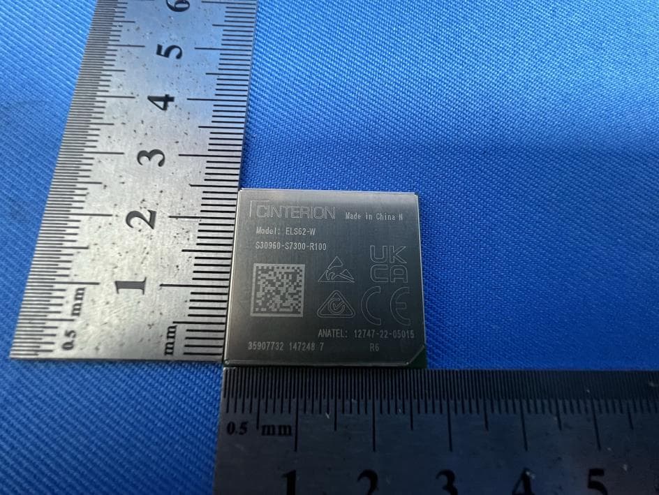
QIPELS62-W
Oct 09, 2023IoT Module
Equipment Class
PCB - PCS Licensed Transmitter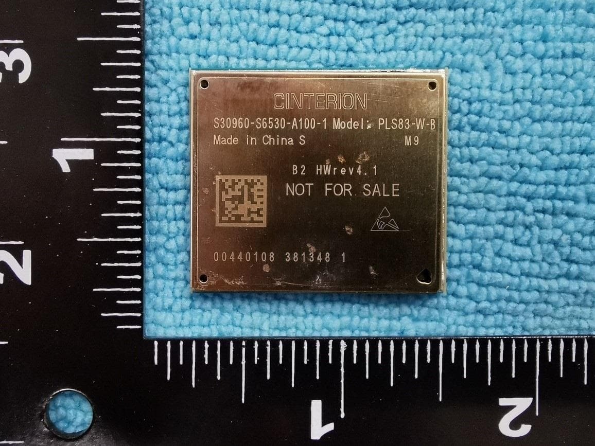
QIPPLS83-W-B
Nov 22, 2022Module
Equipment Class
JBP - Part 15 Class B Computing Device Peripheral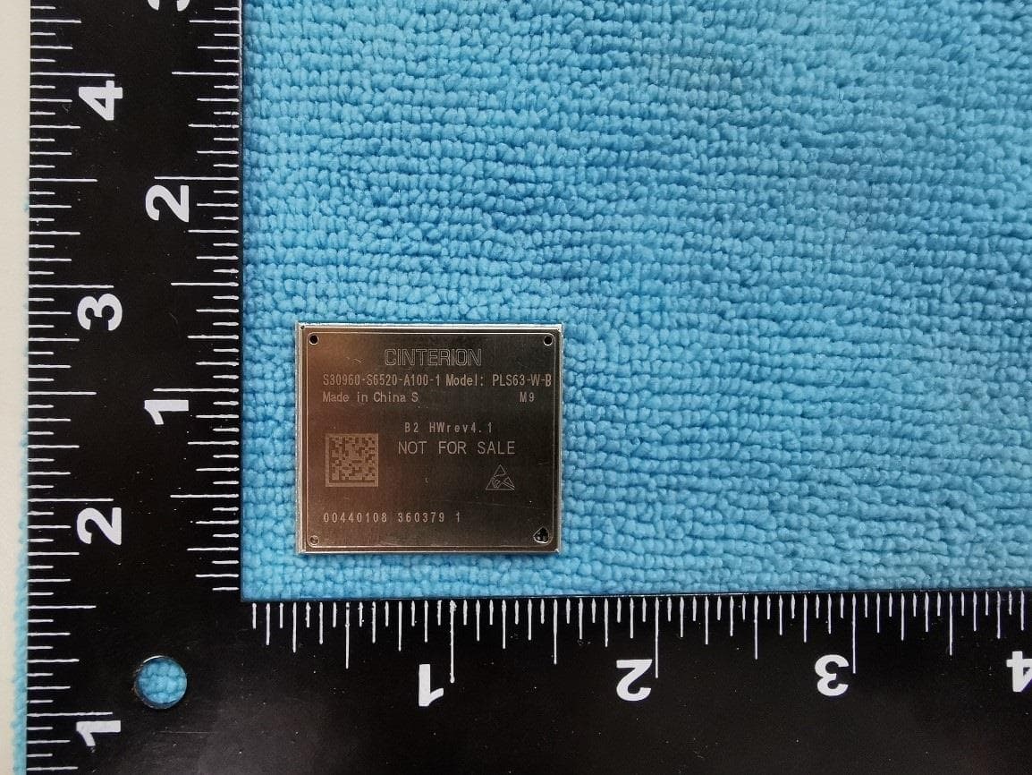
QIPPLS63-W-B
Nov 22, 2022Module
Equipment Class
PCB - PCS Licensed Transmitter
QIPPLS63-X-B
Nov 10, 2022Module
Equipment Class
PCB - PCS Licensed Transmitter
QIPPLS83-X-B
Nov 06, 2022Module
Equipment Class
JBP - Part 15 Class B Computing Device Peripheral