QIPTC65Quadband GSM/GPRS Module
Telit Cinterion Deutschland GmbH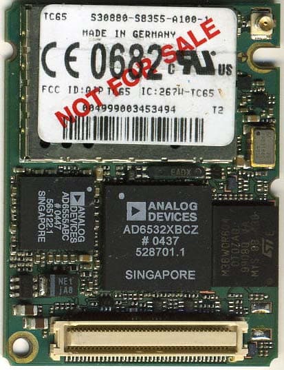
Click to zoom
Application Details
- Equipment Class
- PCB - PCS Licensed Transmitter
- Date of Grant
- Jun 09, 2005
- Application Purpose
- Original Equipment
- Date of Application
- Jun 09, 2005
- Equipment Note
- Quadband GSM/GPRS Module
- Frequency Range
- 824.20000000 - 848.80000000
- Country
- Germany
Documents & Files
Document Text
Text extracted from the exhibit documents filed with the FCC. Open a document above to read the original.
Users Manual
Hardwa r e Interface Descri p tion TC65 Siemens Cellular Engine Version: 00.450 DocID: TC65_HD_V00.450 s TC65 Hardware Interface Description Strictly confidential / Draft s TC65_HD_V00.450 Page 2 of 96 20.04.2005 Document Name: TC65 Hardware Interface Description Version: 00.450 Date: April 20, 2005 DocId: TC65_HD_V00.450 Status: Strictly confidential / Draft General note Product is deemed accepted by Recipient and is provided without interface to Recipient ́s products. The Product constitutes pre-release version and code and may be changed substantially before commercial release. The Product is provided on an “as is” basis only and may contain deficiencies or inadequacies. The Product is provided without warranty of any kind, express or implied. To the maximum extent permitted by applicable law, Siemens further disclaims all warranties, including without limitation any implied warranties of merchantability, fitness for a particular purpose and noninfringement of third-party rights. The entire risk arising out of the use or performance of the Product and documentation remains with Recipient. This Product is not intended for use in life support appliances, devices or systems where a malfunction of the product can reasonably be expected to result in personal injury. Applications incorporating the described product must be designed to be in accordance with the technical specifications provided in these guidelines. Failure to comply with any of the required procedures can result in malfunctions or serious discrepancies in results. Furthermore, all safety instructions regarding the use of mobile technical systems, including GSM products, which also apply to cellular phones must be followed. Siemens AG customers using or selling this product for use in any applications do so at their own risk and agree to fully indemnify Siemens for any damages resulting from illegal use or resale. To the maximum extent permitted by applicable law, in no event shall Siemens or its suppliers be liable for any consequential, incidental, direct, indirect, punitive or other damages whatsoever (including, without limitation, damages for loss of business profits, business interruption, loss of business information or data, or other pecuniary loss) arising out the use of or inability to use the Product, even if Siemens has been advised of the possibility of such damages. Subject to change without notice at any time. Copyright Transmittal, reproduction, dissemination and/or editing of this document as well as utilization of its contents and communication thereof to others without express authorization are prohibited. Offenders will be held liable for payment of damages. All rights created by patent grant or registration of a utility model or design patent are reserved. Copyright © Siemens AG 2005 TC65 Hardware Interface Description Strictly confidential / Draft s TC65_HD_V00.450 Page 3 of 96 20.04.2005 Contents 0 Document History .........................................................................................................7 1 Introduction ...................................................................................................................8 1.1 Related Documents ...............................................................................................8 1.2 Terms and Abbreviations .......................................................................................9 1.3 Type Approval......................................................................................................12 1.4 Safety Precautions...............................................................................................14 2 Product Concept .........................................................................................................16 2.1 Key Features at a Glance ....................................................................................16 2.2 TC65 System Overview .......................................................................................19 2.3 Circuit Concept ....................................................................................................20 3 Application Interface...................................................................................................21 3.1 Operating Modes .................................................................................................22 3.2 Power Supply.......................................................................................................24 3.2.1 Minimizing Power Losses ......................................................................24 3.2.2 Measuring the Supply Voltage V BATT+ ....................................................25 3.2.3 Monitoring Power Supply by AT Command ...........................................25 3.3 Power Up / Power Down Scenarios.....................................................................26 3.3.1 Turn on TC65.........................................................................................26 3.3.1.1 Turn on TC65 Using Ignition Line IGT ...................................................26 3.3.1.2 Turn on TC65 Using the VCHARGE Signal...........................................28 3.3.1.3 Reset TC65 via AT+CFUN Command ...................................................29 3.3.1.4 Reset TC65 in Case of Emergency via EMERG_RST ..........................29 3.3.2 Turn off TC65.........................................................................................30 3.3.2.1 Turn off TC65 Using AT Command .......................................................30 3.3.2.2 Leakage Current in Power Down Mode .................................................31 3.3.3 Automatic Shutdown ..............................................................................32 3.3.3.1 Temperature Dependent Shutdown.......................................................32 3.3.3.2 Temperature Control during Emergency call .........................................33 3.3.3.3 Un…
Text truncated - open the document above for the full version.
Users Manual
TC65 Hardware Interface Description Strictly confidential / Draft s TC65_HD_V00.450 Page 49 of 96 20.04.2005 3.11.1 Installing the USB Modem Driver This section assumes you are familiar with installing and configuring a modem under Windows 2000 and Windows XP. As both operating systems use multiple methods to access modem settings this section provides only a brief summary of the most important steps. Take care that the “usbmodem.inf” file delivered with TC65 is at hand. Connect the USB cable to the TC65 host application (for example the evaluation board DSB75) and the PC. Windows detects TC65 as a new USB modem, opens the Found New Hardware Wizard and reports that it is searching for the “Siemens AG WM USB Modem” driver. Follow the instructions on the screen and specify the path where the “usbmodem.inf” file is located. Windows will copy the required software to your computer and configure the modem by assigning a free COM port. If you are already using more than one COM port then the next free one will be allocated. Click Finish to complete the installation. Notes for Windows 2000 only: • During the installation procedure you will be prompted for the “usbser.sys” driver. Make sure the file is present before you start installing the above inf file. The “usbser.sys” file is not delivered as a single file, but must be extracted from a Windows 2000 cabinet file. This is either the file “driver.cab” located in the “I386” folder of the original Windows 2000 CD or a later cabinet file inside the Service Pack. SP4 for example includes the “sp4.cab” file which can be found in its “I386” folder. The “usbser.sys” driver from the Service Pack has priority over one provided with the standard Windows 2000 install CD. • It is necessary to restart Windows 2000 to make the changes take effect. TC65 Hardware Interface Description Strictly confidential / Draft s TC65_HD_V00.450 Page 50 of 96 20.04.2005 You can find the “Siemens AG WM USB Modem” listed under Control Panel | Phone and Modem Options | Modems. Troubleshooting for installation problems If Windows fails to assign the next free COM port to TC65 and, for example, allocates a COM port already used by another modem you can manually select a free port as follows: Open the Windows Device Manager, select the installed “Siemens AG WM USB Modem”, click Properties, select the Advanced tab and click Advanced Port settings . From the listbox COM Port Number choose a free port. To make the changes take effect disconnect and re- connect the USB cable. If not yet successful, also restart Windows. TC65 Hardware Interface Description Strictly confidential / Draft s TC65_HD_V00.450 Page 51 of 96 20.04.2005 3.12 I 2 C Interface I 2 C is a serial, 8-bit oriented data transfer bus for bit rates up to 400kbps in Fast mode. It consists of two lines, the serial data line I2CDAT and the serial clock line I2CCLK. The TC65 module acts as a single master device, e.g. the clock I2CCLK is driven by module. I2CDAT is a bi-directional line. Each device connected to the bus is software addressable by a unique 7-bit address, and simple master/slave relationships exist at all times. The module operates as master- transmitter or as master-receiver. The customer application transmits or receives data only on request of the module. To configure and activate the I 2 C bus use the AT^SSPI command. If the I 2 C bus is active the two lines I2CCLK and I2DAT are locked for use as SPI lines. Vice versa, the activation of the SPI locks both lines for I 2 C. Detailed information on the AT^SSPI command as well explanations on the protocol and syntax required for data transmission can be found in [1]. The I 2 C interface can be powered from an external supply or via the VEXT line of TC65. If connected to the VEXT line the I 2 C interface will be properly shut down when the module enters the Power-down mode. If you prefer to connect the I 2 C interface to an external power supply, take care that VCC of the application is in the range of V VEXT and that the interface is shut down when the PWR_IND signal goes high. See figures below as well as Section 7 and Figure 38. In the application I2CDAT and I2CCLK lines need to be connected to a positive supply voltage via a pull-up resistor. For electrical characteristics please refer to Table 17. GSM module I2CDAT I2CCLK GND I2CDAT I2CCLK GND Application VCC R p R p w VEXT Figure 15: I 2 C interface connected to VCC of application TC65 Hardware Interface Description Strictly confidential / Draft s TC65_HD_V00.450 Page 52 of 96 20.04.2005 GSM module I2CDAT I2CCLK GND I2CDAT I2CCLK GND Application VEXT R p R p Figure 16: I 2 C interface connected to VEXT line of TC65 Note: Good care should be taken when creating the PCB layout of the host application: The traces of I2CCLK and I2CDAT should be equal in length and as short as possible. TC65 Hardware Interface Description Strictly confidential / Draft s TC65_HD_V00.450 Page 53 of 96 20.04.2005 3.13 Audio Interfaces TC65 comprises three audio interfaces available on the board-to-board connector: • Two analog audio interfaces, both with balanced or single-ended inputs/outputs. • Serial digital audio interface (DAI) designed for PCM (Pulse Code Modulation). This means you can connect up to three different audio devices, although only one interface can be operated at a time. Using the AT^SAIC command you can easily switch back and forth. Analog switch Digital Audio Interface Ai r Interface DSP MUX MUX D A MICN2 MICP2 MICN1 MICP1 USC6 USC5 USC4 USC3 USC2 AGND USC0 USC1 D A EPP2 EPN2 EPP1 EPN1 VMIC MUX Figure 17: Audio block diagram To suit different types of accessories the audio interfaces can be configured for different audio modes via the AT^SNFS command. The electrical characteristics of the voiceband part vary with the audio mode. For example, sending and receiving amplification, sidetone paths, noise suppression etc. depend on the selected mode and can be altered with AT commands (except for mode 1). Both …
Text truncated - open the document above for the full version.
External Photos
Siemens Cellular Engine TC65 Photos TC65: component side TC65: component side shielding opened TC65: rear side
ID Label/Location Info
Siemens Cellular Engine TC65 Photos TC65: component side TC65: component side shielding opened
Internal Photos
Siemens Cellular Engine TC65 Photos TC65: component side TC65: component side shielding opened TC65: rear side
Operational Description
www.siemens.com/wm TC65 Wireless Modules TC65 – The m2m Application Platform The new Java ™ -based TC65 is the first product of its kind giving developers a complete hardware and software platform with which to create brand-new m2m applications. But that’s not all – quadband and GPRS class 12 provide top-quality GSM/GPRS connectivity. Thanks to the variety of interfaces included, like GPIOs, I 2 C bus and SPI bus, plus its integrated TCP/IP stack, the TC65 can be utilized in just about any m2m application you can imagine, •Remote metering and remote control systems •Security systems, e.g. alarm systems •Vending machines •POS devices and automatic teller machines •... and many more applications. The TC65 supports IMP 2.0, the new Java ™ profile specially developed for data communication modules. It is downward-compatible with IMP 1.0, which was used in the TC45 - TC65’s predecessor. An on-board ARM processor ensures high-speed data processing, while the quadband technology makes it possible for you to employ the module in any GSM network in the world. Java ™ is a complete software development platform with which to create license-free, hardware-independent applications. Using TC65, product developers can cut down their bill of material costs as well as speed up their time-to-market. Thanks to the IMP 2.0 profile, the TC65 enables simple yet safe over-the-air software updates and data encryption for applications in which security is a top issue. As far as environmental friendliness is concerned, the module is ahead of the times: the TC65 is lead-free, meeting the European requirement on limiting the use of certain hazardous substances in electrical and electronic devices (RoHS). TC65 – The Next Generation Java ™ Module General features •Quadband: 850/900/1800/1900 MHz •GSM release 99 •Output power: • Class 4 (2 W) for EGSM 850 and 900 • Class 1 (1 W) for GSM 1800 and 1900 •AT commands Hayes GSM 07.05 and GSM 07.07 •SIM application toolkit release 99 •Supply voltage range: 3.2 to 4.5 V •Recommended supply voltage: 3.8 +/- 0.2 V •Power consumption: • Power down 50 μA • Sleep mode (registered DRX =6) 3 mA • Talk mode (average) 300 mA • GPRS class 12 (average) 600 mA •Charging control for Lithium batteries •Dimensions: 34 x 45 x 3.5 mm •Weight < 10 g •Ambient temperature range: – 30 to + 65°C •Automatic switch off at + 75 °C Open application platform features •ARM7 processor •Memory: 400 kbytes (RAM) and 1.7 Mbytes (Flash) •Improved power-saving modes •TCP/IP stack access via AT commands Java ™ features •CLDC 1.1 Hl •J2ME ™ profile IMP 2.0 •Secure data transmission with HTTPS and PKI •Support of TCP, UDP, HTTP, FTP, SMTP, POP3 •Application SW and module FW update over-the-air Specification for GPRS data transmission •Multislot class 12 •PBCCH support •Coding scheme 1 to 4 •Class B mobile station Specification for CSD data transmission •Up to 14.4 kbit/s •V.110 •Non-transparent mode •USSD support Specification for fax • Group 3, class 1 Specification for voice • Triple-rate codec for HR, FR, and EFR • Adaptive multirate AMR • Basic hands-free operation • Echo cancellation • Noise reduction Specification for SMS • Via GSM or GPRS • Point-to-point MO and MT • Text and PDU mode • SMS cell broadcast Approvals • R&TTE, FCC, UL, IC, GCF, PTBRC • Local approvals and network operator certifications Interfaces • Molex 80-pin board-to-board connector • Hirose U.FL 50 ohm antenna connector • Antenna solder pad • Audio: 2 x analog, 1x digital • 2 serial interfaces with the ITU-T V.24 protocol • USB 2.0 full speed • SIM card interface, 3 V, 1.8 V •I 2 C bus and SPI bus • 2 x analog in (ADC) • 1 x analog out (PWM) • 10 GPIOs More about Siemens Wireless Modules at: www.siemens.com/wm Copyright 2005, Siemens AG Wireless Modules Haidenauplatz 1 81667 Munich, Germany Subject to changes in technology, design and availability Order No.: A31001-W25-A308-X-7600 Printed in Germany Java and all Java based marks are trademarks or registered trade- marks of Sun Microsystems, Inc. in the United States and other countries. Technical Data Original size
RF Exposure Info
- 2 - Maximum Permissable Exposure (as specified in Table 1B of 47 CFR 1.1310 – Limits for Maximum Permissable Exposure (MPE), Limits for General Population/Uncontrolled Exposure) Frequency range (MHz) Power density (mW/cm²) 300 – 1,500 f/1500 1,500 – 100,000 1.0 Calculations 850 MHz band Maximum peak output power at antenna input terminal: 31.5 dBm (1.41 W) (see 7 layers test report 4_SIE_0504_GSM_FCCc – FCC ID QIPMC75) Prediction distance R: 20 cm Prediction frequency: 836,4 MHz MPE limit S: 0.5576 mW/cm² Equation OET bulletin 65, page 18, edition 97-01: S = P*G / (4πR²) S = power density P = power input to the antenna G = power gain of the antenna in the direction of interest relative to an isotropic radiator R = distance to to the center of radiation of the antenna) Maximum allowable antenna gain: 2.98 dBi Prediction The maximum allowed MPE value of 0.5576 mW/cm²will be reached in a distance of 20 cm in case that an antenna with an antenna gain of 2,98 dBi would be used. This means that the power density levels in a distance of 20 cm are in accordance with the FCC regulations as long as the used antenna has a gain below 2,98 dBi. - 3 - Calculations 1900 MHz band Maximum peak output power at antenna input terminal: 28.6 dBm (0,7244 W) (see 7 layers test report 4_SIE_0504_GSM_FCCa – FCC ID QIPMC75) Prediction distance R: 20 cm Prediction frequency: 1880 MHz MPE limit S: 1 mW/cm² Equation OET bulletin 65, page 18, edition 97-01: S = P*G / (4πR²) S = power density P = power input to the antenna G = power gain of the antenna in the direction of interest relative to an isotropic radiator R = distance to to the center of radiation of the antenna) Maximum allowable antenna gain: 8.41 dBi Prediction The maximum allowed MPE value of 1 mW/cm² will be reached in a distance of 20 cm in case that an antenna with an antenna gain of 8,41 dBi would be used. This means that the power density levels in a distance of 20 cm are in accordance with the FCC regulations as long as the used antenna has a gain below 8,41 dBi.
Test Report
FCC Measurement/Technical Report on 4_Siem_0504_GSM_FCCd 7 Layers AG Borsigstr. 11 40880 Ratingen Germany Note: The following test results relate only to the devices specified in this document. This report shall not be reproduced in parts without the written approval of the testing laboratory. GSM Module TC63 Siemens Cellular Engine TC63 7 layers AG, Borsigstrasse 11 40880 Ratingen, Germany Phone: +49 (0) 2102 749 0 Fax: +49 (0) 2102 749 350 http://www.7Layers.com Aufsichtsratsvorsitzender - Chairman of the Supervisory Board: Michael Abels Vorstand - Board of Directors: Dr. Hans-Jürgen Meckelburg René Schildknecht Registergericht - registered in: Düsseldorf, HRB 44096 USt-IdNr VAT Nr: DE 203159652 Report Reference: TTI-P-G 178/99 Test Laboratory (Headquarter): Interlab is a registered trademark of 7 layers AG Table of Contents 0. Summary 0.1 Technical Report Summary 0.2 Measurement Summary 1. Administrative Data 1.1 Testing Laboratory 1.2 Project Data 1.3 Applicant Data 1.4 Manufacturer Data 2. Testobject Data 2.1 General EUT Description 2.2 EUT Main Components 2.3 Ancillary Equipment 2.4 EUT Setups 2.5 Operating Modes 3. Test Results 3.1 RF Power Output 3.3 Spurious Emissions at Antenna Terminals 3.2 Frequency Stability 3.4 Field Strength of Spurious Radiation 4. Testequipment 5. Foto Report 6. Setup Drawings 7. Annex 3 3 4 5 5 5 5 5 6 6 7 7 7 7 8 8 11 14 17 19 21 3.5 Emission and Occupied Bandwidth 3.6 Modulation Charcteristics Page 2 of 21Testreport Reference: 4_Siem_0504_GSM_FCCd 0 Summary 0.1 Technical Report Summary Type of Authorization Certification for a broadband PCS device Applicable FCC Rules Prepared in accordance with the requirements of FCC Rules and Regulations as listed in 47 CFR Ch.1 Parts 0 to 19 and Parts 20 to 69 (10-1-98 Edition). The following subparts are applicable to the results in this test report. Part 2 Subpart J - Equipment Authorization Procedures, Certification § 2.1046 Measurement required: RF power output § 2.1049 Measurement required: Occupied bandwidth § 2.1051 Measurement required: Spurious emissions at antenna terminals § 2.1053 Measurement required: Field strength of spurious emission § 2.1055 Measurement required: Frequency stability § 2.1057 Frequency spectrum to be investigated Part 24 Subpart E - Broadband PCS § 24.232 Power and antenna height limits § 24.235 Frequency stability § 24.238 Emission limits Summary Test Results: The EUT complied with all performed tests as listed in chapter 0.2 Measurement Summary. Page 3 of 21Testreport Reference: 4_Siem_0504_GSM_FCCd 1. Administrative Data 1.1 Testing Laboratory Company Name: Address: The test facility is also accredited by the following accreditation organisation: Responsible for Accreditation Scope: 7 Layers AG Borsigstr. 11 40880 Ratingen Germany DAR-Registration no. TTI-P-G 178/99 Dipl.-Ing Bernhard Retka Dipl.-Ing Arndt Stöcker Dipl.-Ing Thomas Hoell This facility has been fully described in a report submitted to the FCC and accepted under the registration number 96716 . - Deutscher Akkreditierungs Rat 2005-05-02 Dipl.-Ing. Robert Machulec 2005-05-06 2005-05-02 Responsible for testing and report Receipt of EUT: Date of Test(s): Date of Report: 1.2 Project Data Siemens AG (BLN) Thorsten Liebig Siemensdamm 50 13629 Berlin Germany please see Applicant data 1.4 Manufacturer Data Company Name: Address: Contact Person: Company Name: Address: Contact Person: 1.3 Applicant Data Page 5 of 21Testreport Reference: 4_Siem_0504_GSM_FCCd 2. Testobject Data Type Designation: Kind of Device: (optional) Voltage Type: Nominal Voltage: Equipment under Test: Siemens Cellular EngineTC63 GSM 850/900/1800/1900 GSM Module TC63 DC 4.5 V Ports 2.1 General EUT Description General product description: GSM module for mobile phones which is able to operate in the bands 850, 900, 1800 and 1900. The manufacturer declared that nominal voltage is equal to high voltage. The EUT provides the following ports: Maximum Voltage: Minimum Voltage: 4.5 V 3.2 V antenna connector enclosure + antenna The main components of EUT are listed and described in Chapter 2.2 Page 6 of 21Testreport Reference: 4_Siem_0504_GSM_FCCd Short Description Equipment under Test Type Designation 2.2 EUT Main components: Type, S/N, Short Descriptions etc. used in this Test Report HW StatusSW StatusSerial No.Date of Receipt Rev.B2.5Rev.00.432IMEI: 355633000010085 2005-05-02TC63GSM ModuleEUT A EUT A is connected to the development board. The SMA antenna connector is provided by the development board. For radiated tests an external antenna will be used additionally.. NOTE: The short description is used to simplify the identification of the EUT in this test report 2.3 Ancillary Equipment Short Description Equipment under Test Type DesignationHW StatusSW StatusSerial No.FCC Id For the purposes of this test report, ancillary equipment is defined as equipment which is used in conjunction with the EUT to provide operational and control features to the EUT. It is necessary to configure the system in a typical fashion, as a customer would normally use it. But never the less Ancillary Equipment can influence the test AE2Development BoardDSB75--B1 0077- AE1Allgon-MiniMAG Dualband Antenna Ordering number: 1140.26 --EMV Referenz Antenne_02 - Setup No.Combination of EUTsDescription 2.4 EUT Setups This chapter describes the combination of EUT's and ancillary equipment used for testing. setup_a01EUT A + AE2setup for spurious emissions conducted test setup_a02EUT A + AE1 + AE2setup for spurious emissions radiated test Op. Mode Description of Operating Modes Remarks 2.5 Operating Modes This chapter describes the operating modes of the EUT's used for testing. op-mode 1Call established on Traffic Channel (TCH) 512, Carrier Frequency 1850,2 MHz 512 is the lowest channel op-mode 2Call established on Traffic Channel (TCH) 661, Carrier Frequency 1880 MHz 661 is a mid channel of the full PCS band (blocks A to F) op-mode 3Call established on Traffic Channel (TCH) 810, Carrier Frequency…
Text truncated - open the document above for the full version.
Test Report
7 layers AG Aufsichtsratsvorsitzenderh Registergerichth registered in: Borsigstrasse 11 Chairman of the Supervisory Board: Düsseldorf, HRB 44096 40880 Ratingen, Germany Michael Abels USt-IdNr h VAT Nr: Phone: +49 (0) 2102 749 0 Vorstandh Board: DE 203159652 Fax: +49 (0) 2102 749 350 Dr. Hans-Jürgen Meckelburg www.7Layers.com René Schildknecht InterLab is a registered trademark of 7 layers AG FCC Measurement/Technical Report on GSM Module TC63 Siemens Cellular Engine TC63 Report Reference: 4_SIEM_0504_GSM_FCCe Test Laboratory: 7 layers AG Borsigstrasse 11 40880 Ratingen Germany email: [email protected] TTI-P-G 178/99 Note: The following test results relate only to the devices specified in this document. This report shall not be reproduced in parts without the written approval of the testing laboratory. Testreport Reference: 4_SIEM_0504_GSM_FCCe Page 2 of 23 Table of Contents 0 Summary 3 0.1 Technical Report Summary 3 0.2 Measurement Summary 4 1 Administrative Data 5 1.1 Testing Laboratory 5 1.2 Project Data 5 1.3 Applicant Data 5 1.4 Manufacturer Data 5 2 Testobject Data 6 2.1 General EUT Description 6 2.2 EUT Main components 7 2.3 Ancillary Equipment 7 2.4 EUT Setups 7 2.5 Operating Modes 7 3 Test Results 8 3.1 Spurious emissions at antenna terminals 8 3.2 Field strength of spurious radiation 11 4 Test Equipment 14 5 Photo Report 17 6 Setup Drawings 21 7 Annex 23 Testreport Reference: 4_SIEM_0504_GSM_FCCe Page 3 of 23 0 Summary 0.1 Technical Report Summary Type of Authorization Certification for a GSM cellular radiotelephone device Applicable FCC Rules Prepared in accordance with the requirements of FCC Rules and Regulations as listed in 47 CFR Ch.1 Parts 0 to 19 and Parts 20 to 69 (10-1-01 Edition). The following subparts are applicable to the results in this test report. Part 2 Subpart J - Equipment Authorization Procedures, Certification § 2.1046 Measurement required: RF power output § 2.1049 Measurement required: Occupied bandwidth § 2.1051 Measurement required: Spurious emissions at antenna terminals § 2.1053 Measurement required: Field strength of spurious emission § 2.1055 Measurement required: Frequency stability § 2.1057 Frequency spectrum to be investigated Part 22 Subpart H – Cellular Radiotelephone Service § 22.355 Frequency tolerance § 22.913 Effective radiated power limits § 22.917 Emission limitations for cellular Summary Test Results: The EUT complied with all performed tests as listed in chapter 0.2 Measurement Summary. Testreport Reference: 4_SIEM_0504_GSM_FCCe Page 5 of 23 1 Administrative Data 1.1 Testing Laboratory Company Name: 7 Layers AG Address Borsigstr. 11 40880 Ratingen Germany This facility has been fully described in a report submitted to the FCC and accepted under the registration number 96716 . The test facility is also accredited by the following accreditation organisation: - Deutscher Akkreditierungs Rat DAR-Registration no. TTI-P-G 178/99 Responsible for Accreditation Scope: Dipl.-Ing. Bernhard Retka Dipl.-Ing. Arndt Stöcker Dipl.-Ing. Thomas Hoell Report Template Version: 2005-04-20 1.2 Project Data Responsible for testing and report: Dipl.-Ing. Robert Machulec Receipt of EUT: 2005-05-02 Date of Test(s): 2005-05-02 Date of Report: 2005-05-06 1.3 Applicant Data Company Name: Siemens AG Address: Siemensdamm 50 13629 Berlin Germany Contact Person: Thorsten Liebig 1.4 Manufacturer Data Company Name: please see applicant data Address: Contact Person: Testreport Reference: 4_SIEM_0504_GSM_FCCe Page 6 of 23 2 Testobject Data 2.1 General EUT Description Equipment under GSM Module TC63 Type Designation: Siemens Cellular Engine TC63 Kind of Device: (optional) GSM 850/900/1800/1900 Voltage Type: DC Nominal Voltage: 4,5 V Maximum Voltage: 4,5 V Minimum Voltage: 3,2 V General product description: GSM module for mobile phones which is able to operate in the bands 850, 900, 1800 and 1900. The manufacturer declared that nominal voltage is equal to high voltage. In GSM 850 mode the card operates in channel blocks A and B from 824,2 MHz (lowest channel = 128) to 848,8 MHz (highest channel = 251). The EUT provides the following ports: Ports antenna connector enclosure The main components of the EUT are listed and described in Chapter 2.2 Testreport Reference: 4_SIEM_0504_GSM_FCCe Page 7 of 23 2.2 EUT Main components Type, S/N, Short Descriptions etc. used in this Test Report Short Description Equipment under Test Type Designation Serial No. HW Status SW Status Date of Receipt EUT A GSM Phone TC63 3556330000 10085 Rev.B2.5 Rev.00.432 2005-05-02 Remark: EUT A is connected to the development board. The SMA antenna connector is provided by the development board. For radiated tests an external antenna will be used additionally. NOTE: The short description is used to simplify the identification of the EUT in this test report. 2.3 Ancillary Equipment For the purposes of this test report, ancillary equipment is defined as equipment which is used in conjunction with the EUT to provide operational and control features to the EUT. It is necessary to configure the system in a typical fashion, as a customer would normally use it. But nevertheless Ancillary Equipment can influence the test results. Short Description Equipment under Test Type Designation HW Status SW Status Serial no. FCC ID AE1 Allgon- MiniMAG Dualband Antenna Ordering number: 1140.26 – – EMV Referenz Antenne No.02 – AE2 Develop- ment Board DSB75 B1 0077 – 2.4 EUT Setups This chapter describes the combination of EUT's and ancillary equipment used for testing. Setup No. Combination o…
Text truncated - open the document above for the full version.
Contact Information
Applicant
Paolo Schiratti(VP Global Certification)
Test Firm
7layers AGRobert Machulec
Technical Specifications
| # | Rule Parts | Frequency Range | Power Output | Emission | Tolerance |
|---|---|---|---|---|---|
| 2 | 22H | 824.2 MHz - 848.8 MHz | 1.122 W | 300KGXW | 2.5 ppm |
Other Applications from Telit Cinterion Deutschland GmbH
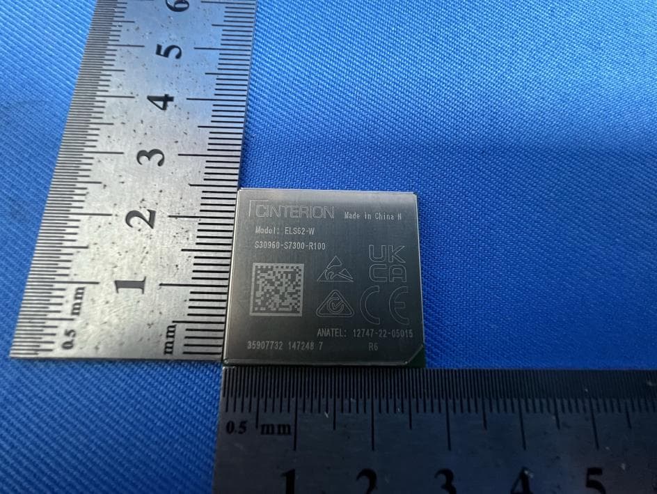
QIPELS62-W
Oct 09, 2023IoT Module
Equipment Class
PCB - PCS Licensed Transmitter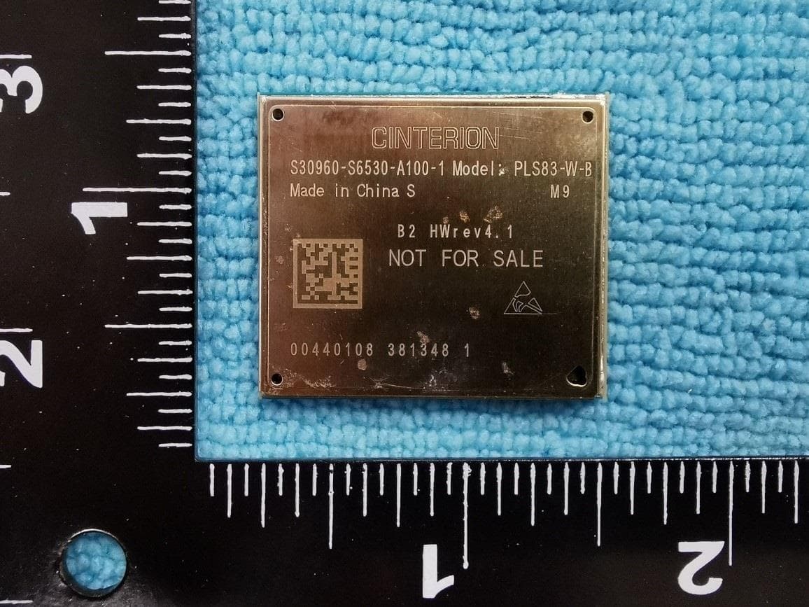
QIPPLS83-W-B
Nov 22, 2022Module
Equipment Class
JBP - Part 15 Class B Computing Device Peripheral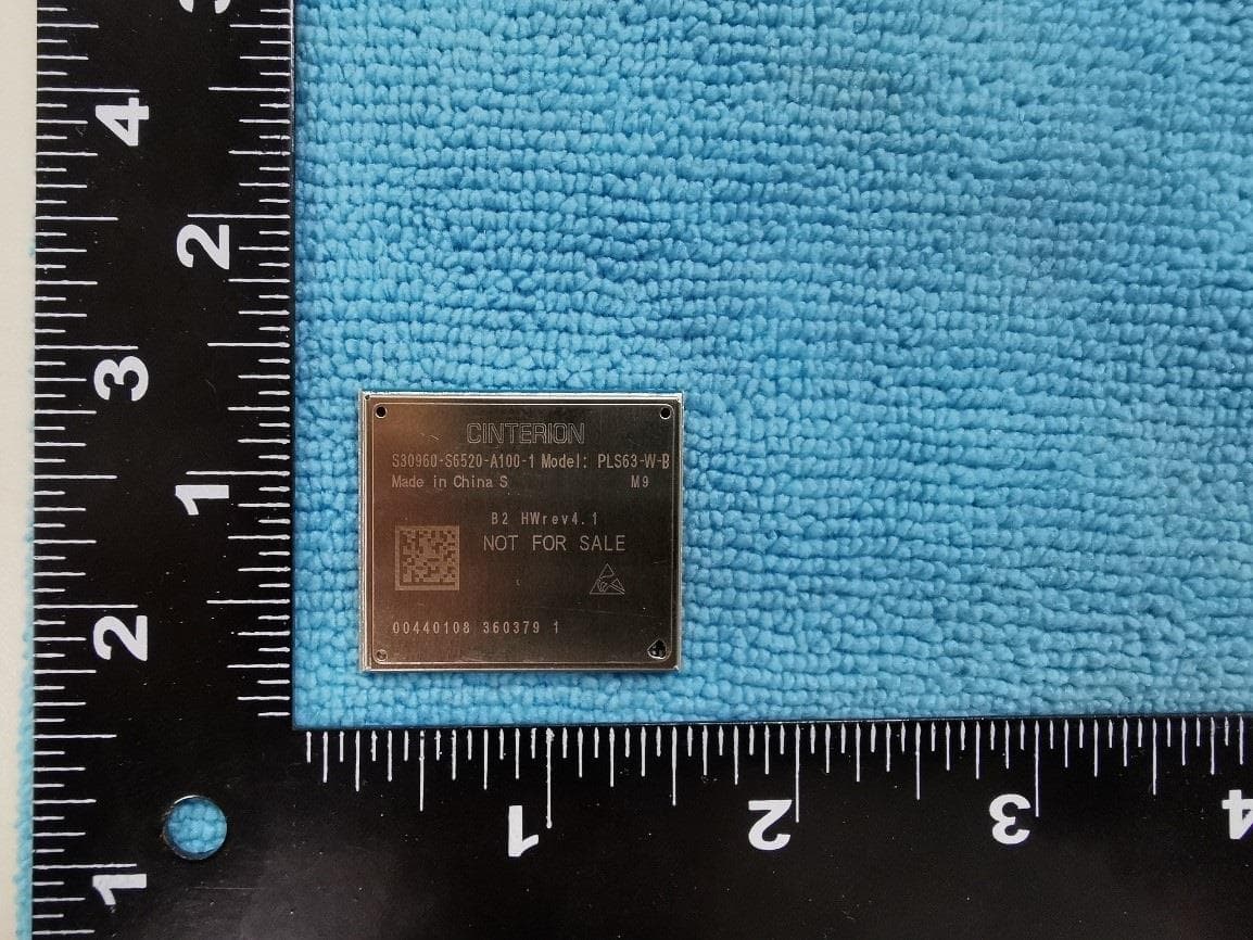
QIPPLS63-W-B
Nov 22, 2022Module
Equipment Class
PCB - PCS Licensed Transmitter
QIPPLS63-X-B
Nov 10, 2022Module
Equipment Class
PCB - PCS Licensed Transmitter
QIPPLS83-X-B
Nov 06, 2022Module
Equipment Class
JBP - Part 15 Class B Computing Device Peripheral