QS3WBPRP1PURE PCI WIRELESS LAN CARD
TwinMOS Technologies Inc.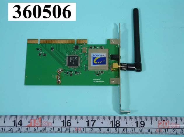
Click to zoom
Application Details
- Equipment Class
- DTS - Digital Transmission System
- Date of Grant
- Jul 14, 2003
- Application Purpose
- Original Equipment
- Date of Application
- Jul 14, 2003
- Equipment Note
- PURE PCI WIRELESS LAN CARD
- Frequency Range
- 2412.00000000 - 2462.00000000
- Company
- TwinMOS Technologies Inc.
- Country
- Taiwan
Documents & Files
Document Text
Text extracted from the exhibit documents filed with the FCC. Open a document above to read the original.
Users Manual
TwinMOS Booming 802.11b Wireless LAN Card User’s Manual TwinMOS ® Booming TwinMOS Page 1 Contents PACKAGE CONTENTS..............................................................2 INTRODUCTION..........................................................................3 WIRELESS NETWORK OVERVIEW............................................4 BOOMING WIRELESS NETWORK SCENARIOS...........6 INSTALLATION FOR LINUX .................................................................................9 INSTALLATION FOR WINDOWS..................................................11 CONFIGURATION UTILITY.........................................................19 TROUBLESHOOTING.........................................................27 TECHNICAL SPECIFICATIONS............................................28 FCC CAUTION ........................................................................................39 Booming TwinMOS Page 2 PACKAGE CONTENTS Unpack your Booming WLAN Card kit and verify that all items are present. z Booming Wireless LAN card z User’s Manual (on CD) z Driver (on CD) If any of the items described appear to be damaged or missing, please contact your reseller. Booming TwinMOS Page 3 INTRODUCTION The Booming WLAN Card is a wireless network client that complies with the IEEE 802.11b standard on wireless LANs. The IEEE 802.11b standards compliance means this adapter gives you the flexibility to connect it to any 802.11b network. The IEEE 802.11b Ethernet standard allows you to connect computers and devices at speeds up to 11Mbps, dependent upon the distance between wireless adapters, the configuration of your working environment, or the capabilities or limitations of your computer systems. This Booming WLAN Card supports following WLAN features z Automatic transmit data rate select mechanism in the transmit range of 1, 2, 5.5 and 11 Mbps. z Center frequency channel selection (2.4 GHz) z Roaming over multiple channels. z Supports power save mode z Support TKIP and AES advanced WLAN security z 128-bit Wired Equivalent Privacy (WEP) data encryption. This Booming WLAN card comes with software drivers for the most popular Microsoft Windows operating systems and can be integrated into a larger network, running Windows XP, Windows 2000, Windows ME, or Windows 98 in either Ad-Hoc mode or infrastructure mode. This manual provides a quick introduction to wireless technology and its application as it relates to networking. Take a moment to read through this manual and familiarize you with wireless technology. You should also give yourself some time to become familiar with your new wireless network. Booming TwinMOS Page 4 WIRELESS NETWORK OVERVIEW A wireless local area network (LAN) is a flexible data communications system implemented as an extension to, or as an alternative for, a wired LAN. Using radio frequency (RF) technology, wireless LANs transmit and receive data over the air, minimizing the need for wired connections. Thus, wireless LANs combine data connectivity with user mobility. A local area network that transmit and receive over the air typically in an unlicensed frequency such as the 2.4GHz band. A wireless LAN does not require lining up devices for line of sight transmission like IrDA. Wireless access points (base stations) are connected to an Ethernet hub or server and transmit a radio frequency over an area of several hundred to a thousand feet which can penetrate walls and other nonmetal barriers. Roaming users can be handed off from one access point to another like a cellular phone system. Laptops use wireless modems that plug into an existing Ethernet port or that are self contained on PC cards, while stand-alone desktops and servers use plug-in cards (ISA, PCI, etc.). Wireless LANs offer the following productivity, convenience, and cost advantages over traditional wired networks Mobility - WLAN provide LAN users to access data in any location within the operating range of the WLAN. Ad-hoc management decisions based on real-time information can significantly improve worker efficiency. Installation Speed and Simplicity - Installing a wireless LAN system can be fast and easy and can eliminate the need to pull cable through walls and ceilings. Installation Flexibility - Wireless technology allows the network to go where wire cannot go. Reduced Cost-of-Ownership - While the initial investment required for wireless LAN hardware can be higher than the cost of wired LAN hardware, overall installation expenses and life-cycle costs can be significantly lower. Long-term cost benefits are greatest in dynamic environments requiring frequent moves and changes. Scalability - Wireless LAN systems can be configured in a variety of topologies to meet the needs of specific applications and installations. Configurations are easily changed and range from peer-to-peer networks suitable for a small number of users to full infrastructure networks of thousands of users that enable roaming over a broad area. Installation Considerations Designed to go up to 300 feet (100 meters) indoors and up to 900 feet (273 meters) outdoors, Booming WLAN card lets you access your network from virtually anywhere you want. Keep in mind, however, that the number and thickness of walls, ceilings or other objects that the wireless signals must pass thru may limit range. Typical ranges vary depending on the types of materials and background RF noise in your home or business. The key to maximizing range is to follow these basic principles: Booming TwinMOS Page 5 Keep the number of walls and ceilings between the access point and your receiving device to a minimum - Each wall or ceiling can reduce your TwinMOS Booming Wireless product’s range from 3-90 feet (1-30 meters.) For some businesses or for a large residential home deployment, it may be more beneficial to have more than one access point with overlapping coverage. 1. Be aware of the direct line between Access Points, Residential Gateways, and Computers - A wall that is 1.5 feet th…
Text truncated - open the document above for the full version.
Block Diagram
Philips SemiconductorsProduct data SA2400ASingle chip transceiver for 2.45 GHz ISM band 2002 Nov 04 BLOCK DIAGRAM AGC STATE MACHINE 2 RF_IN 2 RSSI A/D 2 RX_OUT_I RSSI RX_OUT_Q AGCSET AGCRESET 0 90 CONTROL SEN SCLK SDATA TXRX TX_HI FILTER TUNING 0 90 (2.4GHz) TX_OUT_HI TX_OUT_LO 2 POWER DETECTOR A/D TXCAL STATE MACHINE PLL CP :2 D/A V_TUNE XTAL D/A XO REF_CLK 2 LOCK FIRDAC FIRDAC TX_IN_I DATA_I DATA_Q TX_IN_Q 2 2 SR02386 Figure 1. SA2400A functional block diagram.
External Photos
FCC ID: QS3WBPRP1 Number1 FRONT SIDE OF EUT FCC ID: QS3WBPRP1 Number2 REAR SIDE OF EUT
ID Label/Location Info
FCC ID: QS3WBPRP1
Internal Photos
FCC ID: QS3WBPRP1 Number1 FRONT SIDE OF EUT FCC ID: QS3WBPRP1 Number2 REAR SIDE OF EUT
Operational Description
FCC ID: QS3WBPRP1 Operational Description The transmitter of the EUT (2.4GHz WLAN PCI Card ) is powered by PCI interface. The antenna is Dipole Antenna, and the antenna connector type is SMA. The other instruction, please have a look at the users manual. DSSS Information This device is Direct Sequence Spread Spectrum, the data is mixed by pseudorandom code which is an orthogonal code. The mixed data is digital modulated by BPSK and QPSK technique depends on the data rates. The CCK coding is applied for increasing the data rate, and also the processing gain will be increased. It is capable of processing packets that are encording to IEEE Std 802.11 and IEEE Std 802.11b high-rate extension ( 1- and 2-Mbit/s Barker, 5.5- and 11-Mbit/s CCK and PBCC). The bit rates are 1,2,5.5,11Mbps in the Barker and CCK encoder mode, the symbol rates are 1,1,1.375,1.375Mbps. The chip rates are always 11Mbps. So, the Chip/symbol is 11, and 8 respectively. Although is higher bit rate, the processing gain is lower than 10, but the CCK and PBCC coding used in higher bit rate will provide 2.2dB coding gain.
Schematics
Spec Name Engineering Run Output Of RealTEK 8180 Pure PCI WLAN Card Page 1 of 5 Spec No. D-W0302-DE-1.0 Rev. 1.0 The information contained herein is the exclusive property of TwinMOS Technologies Inc. and shall not be distributed, reproduced, or disclosed in whole or in part without prior written permission of TwinMOS Technologies Inc. CALEN/AGCRESET IFLE/AGCSET PAPE ANTSEL+ ANTSEL- TRSW+ TRSW- RFLE RIFSD RIFSCK PE2/AUX TXDET RF_TXI+RF_TXI-RF_RXI+RF_RXI-RF_RXQ+RF_RXQ- RF_REF_IN RF_TXQ-RF_TXQ+ RF_REF_OUT TX/RXXTAL_1 BB2RFBB2RF.sch REQBCLKSERRBDEVSELBCBE2BCLKRUNBRSTBAD[0..31]CBE3BINTABCBE1BGNTBSTOPBFRAMEBCBE0BIRDYBPARPERRBCSTCHGTRDYBPMEBVMAINIDSELLED/HOTKEY cardbusi&powercardbus&power.sch AD[0..31] RSTB CBE3BCBE2B FRAMEB IRDYB TRDYB DEVSELB STOPB PERRBSERRB PAR CBE1BCBE0B PE1/PHITXQBB_RXQ-BB_RXQ+BB_RXI-TXDETBB_TXQ-RIFSCKRIFSDRFLEIFLE/AGCSETCALEN/AGCRESET CLKRUNB BB_TXI+BB_TXI-BB_TXQ+BB_RXI+PE2/AUXANTSEL-TRSW+PAPETRSW-VCOPDN/PHITXI/9356SELANTSEL+ CSTCHG GNTB INTAB CLK REQBPMEB VMAIN RF_REF_IN IDSEL RF_REF_OUT LED/HOTKEY LED/HOTKEY RTL8180-QFP128RTL8180-QFP128.sch BB_TXI+ BB_TXI- BB_RXI+ BB_RXI- BB_RXQ+ BB_RXQ- BB_TXQ+ BB_TXQ- RF_RXI+RF_RXI-RF_RXQ+RF_RXQ-RF_TXI+RF_TXI-RF_TXQ+RF_TXQ- VCOPD/PHITXI/9356SEL PE1/PHITXQ RF_REF_IN PE2/AUX XTAL_1TX/RX LED/HOTKEY PhilipRFPhilipRF.sch Spec Name Engineering Run Output Of RealTEK 8180 Pure PCI WLAN Card Page 2 of 5 Spec No. D-W0302-DE-1.0 Rev. 1.0 The information contained herein is the exclusive property of TwinMOS Technologies Inc. and shall not be distributed, reproduced, or disclosed in whole or in part without prior written permission of TwinMOS Technologies Inc. BB_TXI+ BB_TXI- BB_RXI+ BB_RXI- BB_RXQ+ BB_RXQ- BB_TXQ+ BB_TXQ- T2TPT3TP T7TP T8TP DR782 (1%) DR220 DR682 (1%) DR21390(1%) DR230 DC10 Note 4NP DC3 Note4NPDC4 Note 4NP T4TPT5TP T9TP T10TP DR982 (1%) DR260 DR882 (1%) DR25390 (1%) DR270 DC12 Note4NP DC6 Note 4NPDC7 Note4NP RF_RXI+ RF_RXI- RF_RXQ+ RF_RXQ- RF_TXI+ RF_TXI- RF_TXQ+ RF_TXQ- DR50DR100 VCOPD/PHITXI/9356SEL PE1/PHITXQ AGNDAGND AGNDAGND AGND AGND Note3 Spec Name Engineering Run Output Of RealTEK 8180 Pure PCI WLAN Card Page 3 of 5 Spec No. D-W0302-DE-1.0 Rev. 1.0 The information contained herein is the exclusive property of TwinMOS Technologies Inc. and shall not be distributed, reproduced, or disclosed in whole or in part without prior written permission of TwinMOS Technologies Inc. CC310nF + CC144.7uF CC1210nF + CC134.7uF LL4 SBK201209T-700Y S LL3 SBK201209T-700Y S N/ C 4 G R OUND 2 IN P U T 1 SH T D N 3 OUT P U T 5 UU1XC6209B302M R + CC1547uF CC610nF V D D 2400 + CC174.7uF CC810nF LL2 SBK201209T-700Y S + CC1647uF CC710nF V D D 2411 CC410nF CC910nF + CC184.7uF LL5 SBK201209T-700Y S N/ C 4 G R OUND 2 IN P U T 1 SH T D N 3 OUT P U T 5 UU3XC6204B182M R + CC194.7uF CC1110nF CC1010nF VDD1 8 VDD3 3 V C C 33.3 RR2 0 RR10 RR3 0 RR4 0 T6TP RE QB S E RRB DE VS E L B CL K RS T B A D [ 0..31] CBE 3 B ST O P B FR A M EB CBE 2 B T R DYB ID S E L VCC3 3 VCC3 3 +D C 1 47U F IN T A B DC20.1u CBE 1 B GN T B CBE 0 B I R DYB PA R P E RRB PMEB A D [ 0..31] DR5 3 No t e 1 0 RR5 No t e 4 0 LL6 SBK201209T-700Y S 4.7uF = > 47uF 10uF = > 47uF O p tio n : C o n n e c t R R 5 to b y p a s s 3 . 0 V re g u la to r CC2110nF + CC244.7uF N/ C 4 G R OUND 2 IN P U T 1 SH T D N 3 OUT P U T 5 UU7XC6209B302M R + CC2347uF CC2210nF V C C 33.3 LL8 SBK201209T-700Y S CC2010nF RR7 No t e 4 0 4.7uF = > 47uF O p tio n : C o n n e c t R R 7 to b y p a s s 3 . 0 V re g u la to r VCC3 3 DR0 0 TR S T # A1 - 12V B1 + 12V A2 TC K B2 TM S A3 G r o und B3 TD I A4 TD O B4 +5 V A5 +5 V B5 IN T A # A6 +5 V B6 IN T C # A7 IN T B # B7 +5 V A8 IN T D # B8 Reser v ed A9 PR SN T 1 # B9 + 3 . 3 V( I / O) A1 0 Reser v ed B1 0 Reser v ed A1 1 PR SN T 2 # B1 1 KE Y A1 2 KE Y B1 2 KE Y A1 3 KE Y B1 3 3.3V a u x A1 4 Reser v ed B1 4 RS T # A1 5 G r o und B1 5 +3 . 3 V A1 6 CL K B1 6 GN T # A1 7 G r o und B1 7 G r o und A1 8 RE Q# B1 8 PME# A1 9 +3 . 3 V B1 9 AD[ 3 0 ] A2 0 AD[ 3 1 ] B2 0 +3 . 3 V A2 1 AD[ 2 9 ] B2 1 AD[ 2 8 ] A2 2 G r o und B2 2 AD[ 2 6 ] A2 3 AD[ 2 7 ] B2 3 G r o und A2 4 AD[ 2 5 ] B2 4 AD[ 2 4 ] A2 5 +3 . 3 V B2 5 ID S E L A2 6 C/ BE [ 3 ] # B2 6 +3 . 3 V A2 7 AD[ 2 3 ] B2 7 AD[ 2 2 ] A2 8 G r o und B2 8 AD[ 2 0 ] A2 9 AD[ 2 1 ] B2 9 G r o und A3 0 AD[ 1 9 ] B3 0 AD[ 1 8 ] A3 1 +3 . 3 V B3 2 AD[ 1 6 ] A3 2 AD[ 1 7 ] B3 2 +3 . 3 V A3 3 C/ BE [ 2 ] # B3 3 FR A M E# A3 4 G r o und B3 4 G r o und A3 5 I R DY# B3 5 T R DY# A3 6 +3 . 3 V B3 6 G r o und A3 7 DE VS E L # B3 7 ST O P # A3 8 PC I X C A P B3 8 +3 . 3 V A3 9 LO C K # B3 9 S M BCL K A4 0 P E RR# B4 0 S M BDAT A4 1 +3 . 3 V B4 1 G r o und A4 2 S E RR# B4 2 PA R A4 3 +3 . 3 V B4 3 AD[ 1 5 ] A4 4 C/ BE [ 1 ] # B4 4 +3 . 3 V A4 5 AD[ 1 4 ] B4 5 AD[ 1 3 ] A4 6 G r o und B4 6 AD[ 1 1 ] A4 7 AD[ 1 2 ] B4 7 Gr o u m d A4 8 AD[ 1 0 ] B4 8 AD[ 0 9 ] A4 9 M 66E N B4 9 G r o und A5 0 G r o und B5 0 G r o und A5 1 G r o und B5 1 C/ BE [ 0 ] # A5 2 ADD[ 0 8 ] B5 2 +3 . 3 V A5 3 AD[ 0 7 ] B5 3 AD[ 0 6 ] A5 4 +3 . 3 V B5 4 AD[ 0 4 ] A5 5 AD[ 0 5 ] B5 5 G r o und A5 6 AD[ 0 3 ] B5 6 AD[ 0 2 ] A5 7 G r o und B5 7 AD[ 0 0 ] A5 8 AD[ 0 1 ] B5 8 + 3 . 3 V( I / O) A5 9 + 3 . 3 V( I / O) B5 9 R E Q 64# A6 0 A C K 64# B6 0 +5 V A6 1 +5 V B6 1 +5 V A6 2 +5 V B6 2 P?CONNE CT OR 1 2 4 DR5 2 No t e 1 0 Spec Name Engineering Run Output Of RealTEK 8180 Pure PCI WLAN Card Page 4 of 5 Spec No. D-W0302-DE-1.0 Rev. 1.0 CCMP EEDIEEDOEESKEECS VDD33 IRDYB CLKRUNB TRDYB VDD33 TXQ- AGNDAD0 PAPEVCOPD/PHITXI/9356SEL RXI- AGND INTABVDD18GNTBAD30 AD20 AD1 TRSW+ DGND AGND VDD33 ISOLATEB AD6 RXQ- DGND CBE1B AD4AD7 DGND AD23 PAR AGNDAD8 IFLE/AGCSETRFLE RIFSCK VDD18AD28 CBE3B DGND VDD33 AD2DGND CCMP VDD33 DGND AD10AD12 AVDD33 DGND DEVSELB AD15 TXI-VDD18 TRSW- RIFSD AVDD33 AGND EESKAD31 PERRB SERRB AD14 AD13 CBE0BAD11 AGND TXDET DGND VDD18 DGNDAD9 RXI+ CLKAD25 R10K DGNDISOLATEBVDD33 AVDD33 RSTBREQBAD27AD24 AD16 DGND VDD33 CALEN/AGCRESET R34K AD21 AD17 R34KTXI+ TXQ+ AD3 AVDD33 RXQ+ PE2/AUXEEDOAD29 AD22 PE1/PHITXQ AGND VDDREG AD19 AD18 STOPB AD5 EEDIEECSAD26 R10K CBE2B FRAME…
Text truncated - open the document above for the full version.
Test Report
FCC TEST REPORT Report No. : F360506 SPORTON International Inc. TEL : 886-2-2696-2468 FAX : 886-2-2696-2255 FCC TEST REPORT for 47 CFR, Part 15, Subpart C Equipment : Pure PCI Wireless LAN Card Model No. : 73-TMWBP-002 FCC ID : QS3WBPRP1 Filing Type : Certification Applicant : TwinMOS Technologies Inc. 303 No. 3, Tzu Chiang Rd., Hu Kou Xiang, Hsin Chu, Taiwan, R.O.C. The test result refers exclusively to the test presented test model / sample. Without written approval of SPORTON International Inc., the test report shall not be reproduced except in full. Certificate or Test Report must not be used by the applicant to claim the product in this test report endorsement by NVLAP or any agency of U.S. government. SPORTON International Inc. 6F, No.106, Sec. 1, Hsin Tai Wu Rd., Hsi Chih, Taipei Hsien, Taiwan, R.O.C. FCC TEST REPORT Report No. : F360506 SPORTON International Inc. FCC ID : QS3WBPRP1 TEL : 886-2-2696-2468 Page No. : i FAX : 886-2-2696-2255 Issued Date : Jun. 24, 2003 Table of Contents History of this test report..................................................................................................................ii CERTIFICATE OF COMPLIANCE........................................................................................................................1 1. General Description of Equipment under Test.............................................................................................2 1.1. Applicant..........................................................................................................................................................................................2 1.2. Manufacturer ...................................................................................................................................................................................2 1.3. Basic Description of Equipment under Test ....................................................................................................................................2 1.4. Feature of Equipment under Test ...................................................................................................................................................3 2. Test Configuration of Equipment under Test ...............................................................................................4 2.1. Test Manner ....................................................................................................................................................................................4 2.2. Description of Test System .............................................................................................................................................................4 2.3. Connection Diagram of Test System ..............................................................................................................................................6 3. Operation of Equipment under Test ..............................................................................................................7 4. General Information of Test............................................................................................................................8 4.1. Test Voltage ....................................................................................................................................................................................8 4.2. Standard for Methods of Measurement...........................................................................................................................................8 4.3. Test in Compliance with ..................................................................................................................................................................8 4.4. Frequency Range Investigated .......................................................................................................................................................8 4.5. Test Distance ..................................................................................................................................................................................8 5. Report of Measurements and Examinations ................................................................................................9 5.1. List of Measurements and Examinations ........................................................................................................................................9 5.2. 6dB Bandwidth ..............................................................................................................................................................................10 5.3. Peak Output Power .......................................................................................................................................................................14 5.4. Power Spectral Density .................................................................................................................................................................15 5.5. Test of Conducted Emission .........................................................................................................................................................19 5.6. Test of Radiated Emission ............................................................................................................................................................26 5.7. Band Edges Measurement............................................................................................................................................................57 5.8. Antenna Requirements .................................................................................................................................................................60 5.9. RF Exposure .....................................................................................................................................…
Text truncated - open the document above for the full version.
Test Setup Photos
FCC TEST REPORT Report No. : F360506 SPORTON International Inc. FCC ID : QS3WBPRP1 TEL : 886-2-2696-2468 Page No. : 1 of 3 FAX : 886-2-2696-2255 Issued Date : Jun. 24, 2003 1.1. Photographs of Conducted Emission Test Configuration The photographs show the configuration that generates the maximum emission. FRONT VIEW REAR VIEW FCC TEST REPORT Report No. : F360506 SPORTON International Inc. FCC ID : QS3WBPRP1 TEL : 886-2-2696-2468 Page No. : 2 of 3 FAX : 886-2-2696-2255 Issued Date : Jun. 24, 2003 SIDE VIEW FCC TEST REPORT Report No. : F360506 SPORTON International Inc. FCC ID : QS3WBPRP1 TEL : 886-2-2696-2468 Page No. : 3 of 3 FAX : 886-2-2696-2255 Issued Date : Jun. 24, 2003 1.2. Photographs of Radiated Emission Test Configuration The photographs show the configuration that generates the maximum emission. FRONT VIEW REAR VIEW
Contact Information
Applicant
Sam Hsu(Manager)
Test Firm
Sporton International Inc.Kathy Lin
Technical Specifications
| # | Rule Parts | Frequency Range | Power Output |
|---|---|---|---|
| 1 | 15C | 2.41 GHz - 2.46 GHz | 32.00 mW |
Other Applications from TwinMOS Technologies Inc.

QS3-BTTA01
Oct 01, 2006Bluetooth 2.1ch Audio System for iPod
Equipment Class
DSS - Part 15 Spread Spectrum Transmitter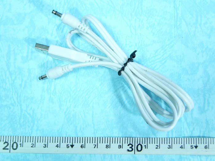
QS3BTT102
Feb 22, 2006Bluetooth Aduio Receiver
Equipment Class
DSS - Part 15 Spread Spectrum Transmitter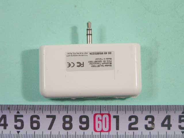
QS3BTT001
Dec 29, 2005Bluetooth Audio Transmitter
Equipment Class
DSS - Part 15 Spread Spectrum Transmitter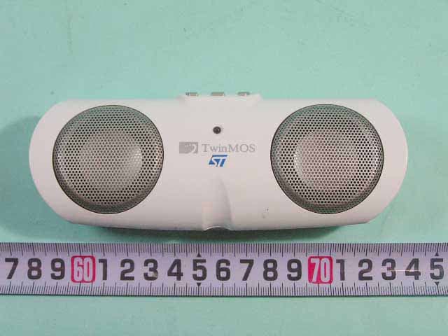
QS3BTT101
Dec 28, 2005Bluetooth Portable Speaker
Equipment Class
DSS - Part 15 Spread Spectrum Transmitter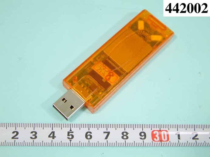
QS3WGSZR1
Oct 31, 2004USB STICK WLAN CARD
Equipment Class
DTS - Digital Transmission System