QT5-RAS26EProfessional 3400/ Professional 5400N
Rimage Corporation
Click to zoom
Application Details
- Equipment Class
- DSS - Part 15 Spread Spectrum Transmitter
- Date of Grant
- Mar 03, 2010
- Application Purpose
- Original Equipment
- Date of Application
- Mar 03, 2010
- Equipment Note
- Professional 3400/ Professional 5400N
- Frequency Range
- 2427.00000000 - 2469.00000000
- Company
- Rimage Corporation
- Country
- United States
Documents & Files
Document Text
Text extracted from the exhibit documents filed with the FCC. Open a document above to read the original.
Users Manual
Rimage Professional™ 3400 and 5400N User Guide 2001431_A Corporate Headquarters: Rimage Corporati on 7725 Washington Avenue South Minneapolis, MN 55439 USA 800-553-8312 (toll free US) Service: +1 952-946-0004 (Asia/Pacifi c, Mexico/Lati n America) Fax: +1 952-944-6956 European Headquarters: Rimage Europe GmbH Albert-Einstein-Str. 26 63128 Dietzenbach Germany Tel: +49-(0) 6074-8521-0 Fax: +49-(0) 6074-8521-100 Rimage Corporati on reserves the right to make improvements to the equipment and soft ware described in this document at any ti me without any prior noti ce. Rimage Corporati on reserves the right to revise this publicati on and to make changes from ti me to ti me in the content hereof without obligati on of Rimage Corporati on to noti fy any person or organizati on of such revisions or changes. This document may contain links to web sites that were current at the ti me of publicati on, but may have moved or become inacti ve since. This document may contain links to sites on the Internet that are owned and operated by third parti es. Rimage Corporati on is not responsible for the content of any such third-party site. ©2010, Rimage Corporati on Rimage ® is a registered trademark of the Rimage Corporati on. Professional™ and Everest™ are trademarks of the Rimage Corporati on. Dell™ is trademark of Dell Computer Corporati on. FireWire™ is a trademark of Apple Computer, Inc. Windows ® is a registered trademark of Microsoft Corporati on. All other trademarks and registered trademarks are the property of their respecti ve owners. 2001431_A 2001431_A Contents Introducti on ....................................................................................................................................... 5 About this User Guide .............................................................................................................................................................. 5 About the Professional 3400 and 5400N ................................................................................................................................. 5 Accessory Kit ............................................................................................................................................................................ 6 Unpacking and Setup Instructi ons ........................................................................................................................................... 6 Important Informati on ....................................................................................................................... 7 Support Informati on ................................................................................................................................................................ 7 Learn More Online ................................................................................................................................................................... 7 Technical Support .................................................................................................................................................................... 7 Opti cal Disc Recording Soft ware Disclaimer ............................................................................................................................ 8 Safety and Compliance Informati on ........................................................................................................................................ 8 Safety Precauti ons ..................................................................................................................................................................................... 8 Country-specifi c Cauti ons and Warnings for Wideband Data Transmission Systems: 2400-2483.5 MHz ................................................. 9 Compliance Informati on ............................................................................................................................................................................ 9 Professional 3400 and 5400N Specifi cati ons ......................................................................................................................... 10 Everest 400 Printer Specifi cati ons .......................................................................................................................................... 12 Printer Requirements ....................................................................................................................... 13 Ribbon Requirements ............................................................................................................................................................ 13 Everest 400 Ribbons ................................................................................................................................................................................ 13 Label Design Requirements ................................................................................................................................................... 14 Print Requirements ................................................................................................................................................................ 14 Identi fy the Parts of the Professional 3400 and 5400N ...................................................................... 15 Front View .............................................................................................................................................................................. 15 Back View ............................................................................................................................................................................... 16 3400 ......................................................................................................................................................................................................... 16 …
Text truncated - open the document above for the full version.
Cover Letter(s)
Tim Dwyer <[email protected]> 5 messages [email protected] <[email protected]>Tue, Mar 2, 2010 at 8:50 PM To: [email protected] Cc: [email protected], [email protected], [email protected] Dear Naoki, You are identified as the contact person for this application. The technical review is complete. There is one issue that must be addressed before this application can be completed. 1. Compliance with the FHSS requirements of FCC 15.247(a)(1), 15.247(g) and 15.247(h) were not documented in the operational description or test report. Please provide additional statements to document compliance with each of these sections. Please note that some sections have more than one requirement. 15.247(a)(1) ....The system shall hop to channel frequencies that are selected at the system hopping rate from a pseudo randomly ordered list of hopping frequencies. Each frequency must be used equally on the average by each transmitter. The system receivers shall have input bandwidths that match the hopping channel bandwidths of their corresponding transmitters and shall shift frequencies in synchronization with the transmitted signals. 15.247(g) Frequency hopping spread spectrum systems are not required to employ all available hopping channels during each transmission. However, the system, consisting of both the transmitter and the receiver, must be designed to comply with all of the regulations in this section should the transmitter be presented with a continuous data (or information) stream. In addition, a system employing short transmission bursts must comply with the definition of a frequency hopping system and must distribute its transmissions over the minimum number of hopping channels specified in this section. 15.247(h) The incorporation of intelligence within a frequency hopping spread spectrum system that permits the system to recognize other users within the spectrum band so that it individually and independently chooses and adapts its hopsets to avoid hopping on occupied channels is permitted. The coordination of frequency hopping systems in any other manner for the express purpose of avoiding the simultaneous occupancy of individual hopping frequencies by multiple transmitters is not permitted The items indicated above must be submitted before processing can continue on the above referenced application. Failure to provide the requested information within 30 days of the original e-mail date may result in application dismissal and forfeiture of the filing fee. Also, please note that partial responses increase processing time and should not be submitted. Any questions about the content of this correspondence should be directed to the e-mail address listed below the name of the sender. Best regards, Tim Dwyer Technical Reviewer UL-CCS [email protected] <[email protected]>Wed, Mar 3, 2010 at 3:35 AM To: [email protected] Cc: [email protected], [email protected], [email protected], [email protected] Dear Mr.Tim Dwyer Hello. I am Aya Hiraga, working for UL Japan, Inc. I am sending this e-mail instead of Naoki. Thank you very much for your comment. We send a document for the pseudorandom frequency hopping sequence. Please confirm an attachment(Pseudorandom Frequency Hopping Sequence.pdf). If there is no further problem, please issue FCC grant with this document. Thank you for your cooperation. Best regards, Aya Hiraga UL Japan, Inc. ----- Forwarded by Naoki Sakamoto/ISE/ULI on 2010/03/03 10:51 ----- <[email protected] > 2010/03/03 10:46 To <[email protected] > cc <[email protected] >, <[email protected]>, <[email protected]> Subject Rimage Corporation, FCC ID: QT5-RAS26E, Assessment NO.: AN10T0150, Notice#1 [Quoted text hidden] - For more information about UL, its Marks, and its services for EMC, quality registrations and product certifications for global markets, please access our web sites at http://www.ul.com and http://www.ul-asia.com or contact your local sales representative. -- ********* Internet E-mail Confidentiality Disclaimer ********** This e-mail message may contain privileged or confidential information. If you are not the intended recipient, you may not disclose, use, disseminate, distribute, copy or rely upon this message or attachment in any way. If you received this e-mail message in error, please return by forwarding the message and its attachments to the sender. UL and its affiliates do not accept liability for any errors, omissions, corruption or virus in the contents of this message or any attachments. ***************************************************************** Pseudorandom Frequency Hopping Sequence.pdf 172K Tim Dwyer <[email protected]>Wed, Mar 3, 2010 at 10:04 AM To: [email protected] Cc: [email protected], [email protected], [email protected], [email protected], Mike Kuo <[email protected]> Dear Aya Hiraga, I have reviewed your attachment. It completes some of the issues I sent in the notice. Several others are still not complete. To help understand the requirements, I have separated the requirements further below. Items with COMPLETE are covered already by your Pseudorandom attachment. For the NOT COMPLETE items, if you make a statement in this email after each item, the email will be submitted with the FCC application as documentaion of compliance. Please understand that FCC requires the TCB to confirm compliance with these requirements. If you include these items in your future FHSS test reports, this will help to delays in processing time. 15.247(a)(1) Q1: ....The system shall hop to channel frequencies that are selected at the system hopping rate from a pseudo randomly ordered list of hopping frequencies. COMPLETE Q2: Each frequency must be used equally on the average by each transmitter. NOT COMPLETE. (Depends on answer to Q4.) Q3: The system receivers shall have input bandwidths that match the hopping channel bandwidths of their corresponding transmit…
Text truncated - open the document above for the full version.
External Photos
External Photo Rimage Corporation Professional 3400/Professional5400N [Model: RAS26/RAS26E] 497.7m 371m 484m Entirety Front External Photo Rimage Corporation Professional 3400/Professional5400N [Model: RAS26/RAS26E] Back(RAS26) Back(RAS26E) Right External Photo Rimage Corporation Professional 3400/Professional5400N [Model: RAS26/RAS26E] Left Top External Photo Rimage Corporation Professional 3400/Professional5400N [Model: RAS26/RAS26E] Bottom
ID Label/Location Info
Label Location Model:RAS26 Label Model:RAS26E Label
Internal Photos
Internal Photo Rimage Corporation Professional 3400/Professional5400N [Model: RAS26/RAS26E] RF Board Front Internal Photo Rimage Corporation Professional 3400/Professional5400N [Model: RAS26/RAS26E] Back Antenna Internal Photo Rimage Corporation Professional 3400/Professional5400N [Model: RAS26/RAS26E]
RF Exposure Info
UL Japan, Inc. Shonan EMC Lab. 1-22-3 Megumigaoka, Hiratsuka-shi, Kanagawa-ken, 259-1220 JAPAN Telephone: +81 463 50 6400 Facsimile: +81 463 50 6401 Applicant: R im age Corporation Type of Equipment : Professional 3400 / Professional 5400N Model No. : RAS26 / RAS26E FCC ID: QT5-RAS26E Rimage Corporation declares that Model : Professional 3400 / Professional 5400N complies with FCC radiation exposure requirement specified in the FCC Rules 2.1091. The “RAS26 / RAS26E“ has 9.02 mW of conducted Peak Output power and 4.52 mW of EIRP. This equipment is considered as a mobile device so that SAR testing is excluded. The Following calculation is the reference data for 20cm distance. RF Ex posure Calculations: T he fo llo w ing info r matio n pr o vides the m inimu m separat io n d ist ance fo r t he hig hest g ain antenna provided with the “RAS26 / RAS26E“ as calculated from FCC OE T Bulletin 65 Appendix A, Table (B) Limits for General Population / Uncontrolled Exposure. This calculation is based on the highest EIRP possible from the system, considering maximum power and antenna gain, and considering a 1.0mW/cm^2 uncontrolled exposure limit. The Friis formula used was: S = (P * G ) / (4* π * r 2 ) Where P = 9.02 mW (M aximum peak output power) G = 0.50 Numerical Antenna gain; equal -3.00 dBi r =20.0 cm For: RAS26 / RAS26ES = 0.000899 mW/cm 2 S =0.008989W/m 2 No. : 30CE0256-HO-01-A RF Exposure / SAR Statement
Test Report
Test Report No.: 30CE0256-SH-01-A Pa ge :19/ 48 Issued date : Februar y 19, 2010 FCC ID :QT5-RAS26E APPENDIX 2: Data of EMI test Test placeUL Japan, Inc. Shonan EMC Lab. No.3 Semi-Anechoic Chamber Date2009/12/29 Temperature / Humidity24 deg.C., 30% Enginee rKenichi Adachi ModeTx, 2427MHz ( M/N: RAS2 6S/N: EP2-13 ) Conducted Emission Calculation:Result[dBuV]=Reading[dBuV]+C.Fac(LISN+Cable)[dB] Limit1(QP) Limit2(AV) N(PK) N(QP/AV) L1(PK) L1(QP/AV) Frequency [MHz] RFI Voltage [dBuV] .1530.2.3.5.7123571020 0 10 20 30 40 50 60 70 80 No. Freq. ReadingReading C.Fac ResultsResultsLimitLimitMarginMargin PhaseCommentNo. Freq. <QP><AV> C.Fac <QP><AV><QP><AV><QP><AV>PhaseCommentNo. [MHz][dBuV][dBuV][dB][dBuV][dBuV][dBuV][dBuV][dB][dB] PhaseComment 10.2295424.312.79.734.022.462.552.528.530.1N 20.3841347.937.99.757.647.658.248.20.60.6N 30.4501725.44.39.735.114.056.946.921.832.9N 40.5879519.613.29.729.322.956.046.026.723.1N 50.7082818.43.69.728.113.356.046.027.932.7N 616.113899.22.910.419.613.360.050.040.436.7N 70.2298926.110.19.735.819.862.552.526.732.7L1 80.3847048.138.09.757.847.758.248.20.40.5L1 90.4501724.74.39.734.414.056.946.922.532.9L1 100.5879518.914.69.728.624.356.046.027.421.7L1 110.7082815.24.09.724.913.756.046.031.132.3L1 1216.127839.84.310.420.214.760.050.039.835.3L1 UL Japan, Inc. Shonan EMC Lab. 1-22-3 Megumigaoka, Hiratsuka-shi, Kanagawa 259-1220 JAPAN Telephone : +81 463 50 6400 Facsimile : +81 463 50 6401 Test Report No.: 30CE0256-SH-01-A Pa ge :20/ 48 Issued date : Februar y 19, 2010 FCC ID :QT5-RAS26E Test placeUL Japan, Inc. Shonan EMC Lab. No.3 Semi-Anechoic Chamber Date2009/12/29 Temperature / Humidity24 deg.C., 30% Enginee rKenichi Adachi ModeTx, ( M/N: RAS2 6S/N: EP2-13 ) Tx, 2469MHz Conducted Emission Tx, 2427MHz Tx, 2449MHz N L Chart Y scale [dBuV] Limit1(QP) Limit2(AV) N L1 Frequency [MHz] RFI Voltage [dBuV] .1530.2.3.5.7123571020 0 10 20 30 40 50 60 70 80 [ PEAK DATA ] Limit1(QP) Limit2(AV) N L1 Frequency [MHz] RFI Voltage [dBuV] .1530.2.3.5.7123571020 0 10 20 30 40 50 60 70 80 [ PEAK DATA ] Limit1(QP) Limit2(AV) N L1 Frequency [MHz] RFI Voltage [dBuV] .1530.2.3.5.7123571020 0 10 20 30 40 50 60 70 80 [ PEAK DATA ] UL Japan, Inc. Shonan EMC Lab. 1-22-3 Megumigaoka, Hiratsuka-shi, Kanagawa 259-1220 JAPAN Telephone : +81 463 50 6400 Facsimile : +81 463 50 6401 Test Report No.: 30CE0256-SH-01-A Pa ge :21/ 48 Issued date : Februar y 19, 2010 FCC ID :QT5-RAS26E Test placeUL Japan, Inc. Shonan EMC Lab. No.3 Semi-Anechoic Chamber Date2009/12/29 Temperature / Humidity24 deg.C., 30% Enginee rKenichi Adachi ModeTx, 2427MHz ( M/N: RAS26 ES/N: EP2-43 ) Conducted Emission Calculation:Result[dBuV]=Reading[dBuV]+C.Fac(LISN+Cable)[dB] Limit1(QP) Limit2(AV) N(PK) N(QP/AV) L1(PK) L1(QP/AV) Frequency [MHz] RFI Voltage [dBuV] .1530.2.3.5.7123571020 0 10 20 30 40 50 60 70 80 No. Freq. ReadingReading C.Fac ResultsResultsLimitLimitMarginMargin PhaseCommentNo. Freq. <QP><AV> C.Fac <QP><AV><QP><AV><QP><AV>PhaseCommentNo. [MHz][dBuV][dBuV][dB][dBuV][dBuV][dBuV][dBuV][dB][dB] PhaseComment 10.2098318.67.39.728.317.063.253.234.936.2N 20.3879944.723.49.754.433.158.148.13.715.0N 30.6873617.51.99.727.211.656.046.028.834.4N 414.1648926.820.910.337.131.260.050.022.918.8N 519.2864410.14.710.520.615.260.050.039.434.8N 621.228937.32.310.718.013.060.050.042.037.0N 70.2098320.17.89.729.817.563.253.233.435.7L1 80.3879945.323.69.755.033.358.148.13.114.8L1 90.3883812.5-1.49.722.28.358.148.135.939.8L1 1014.1648927.021.510.337.331.860.050.022.718.2L1 1119.2864410.45.310.520.915.860.050.039.134.2L1 1221.228937.62.710.718.313.460.050.041.736.6L1 UL Japan, Inc. Shonan EMC Lab. 1-22-3 Megumigaoka, Hiratsuka-shi, Kanagawa 259-1220 JAPAN Telephone : +81 463 50 6400 Facsimile : +81 463 50 6401 Test Report No.: 30CE0256-SH-01-A Pa ge :22/ 48 Issued date : Februar y 19, 2010 FCC ID :QT5-RAS26E Test placeUL Japan, Inc. Shonan EMC Lab. No.3 Semi-Anechoic Chamber Date2009/12/29 Temperature / Humidity24 deg.C., 30% Enginee rKenichi Adachi ModeTx, ( M/N: RAS26 ES/N: EP2-43 ) Conducted Emission Tx, 2469MHz Tx, 2449MHz Tx, 2427MHz N L Chart Y scale [dBuV] Limit1(QP) Limit2(AV) N L1 Frequency [MHz] RFI Voltage [dBuV] .1530.2.3.5.7123571020 0 10 20 30 40 50 60 70 80 [ PEAK DATA ] Limit1(QP) Limit2(AV) N L1 Frequency [MHz] RFI Voltage [dBuV] .1530.2.3.5.7123571020 0 10 20 30 40 50 60 70 80 [ PEAK DATA ] Limit1(QP) Limit2(AV) N L1 Frequency [MHz] RFI Voltage [dBuV] .1530.2.3.5.7123571020 0 10 20 30 40 50 60 70 80 [ PEAK DATA ] UL Japan, Inc. Shonan EMC Lab. 1-22-3 Megumigaoka, Hiratsuka-shi, Kanagawa 259-1220 JAPAN Telephone : +81 463 50 6400 Facsimile : +81 463 50 6401 Test Report No.: 30CE0256-SH-01-A Pa ge :23/ 48 Issued date : Februar y 19, 2010 FCC ID :QT5-RAS26E Test placeUL Japan, Inc. Shonan EMC Lab. No.3 Semi-Anechoic Chamber Date2009/12/29 Temperature / Humidity24 deg.C., 30% Enginee rKenichi Adachi ModeStandby ( M/N: RAS26S/N: EP2-13 ) Conducted Emission Calculation:Result[dBuV]=Reading[dBuV]+C.Fac(LISN+Cable)[dB] Limit1(QP) Limit2(AV) N(PK) N(QP/AV) L1(PK) L1(QP/AV) Frequency [MHz] RFI Voltage [dBuV] .1530.2.3.5.7123571020 0 10 20 30 40 50 60 70 80 No. Freq. ReadingReading C.Fac ResultsResultsLimitLimitMarginMargin PhaseCommentNo. Freq. <QP><AV> C.Fac <QP><AV><QP><AV><QP><AV>PhaseCommentNo. [MHz][dBuV][dBuV][dB][dBuV][dBuV][dBuV][dBuV][dB][dB] PhaseComment 10.2304824.412.69.734.122.362.452.428.330.1N 20.3838947.737.79.757.447.458.248.20.80.8N 30.4502225.14.39.734.814.056.946.922.132.9N 40.5887719.513.09.729.222.756.046.026.823.3N 50.7080218.23.49.727.913.156.046.028.132.9N 616.078579.02.610.419.413.060.050.040.637.0N 70.2304826.310.09.736.019.762.452.426.432.7L1 80.3846648.338.29.758.047.958.248.20.20.3L1 90.4502224.64.19.734.313.856.946.922.633.1L1 100.5887718.814.49.728.524.156.046.027.521.9L1 110.7080215.03.89.724.713.556.046.031.332.5L1 1216.101219.64.210.420.014.660.050.040.035.4L1 UL Japan, Inc. Shonan EMC Lab. 1-22-3 Megumigaoka, Hiratsuka-shi, Kanagawa 259-1220 JAPAN Telephone : +81 463 50 6400 Facsimile : +81 463 50…
Text truncated - open the document above for the full version.
Test Report
Test report No. : 30CE0256-HO-01-A Page : 2 of 48 Issued date : February 19, 2010 FCC ID : QT5-RAS26E UL Japan, Inc. Shonan EMC Lab. 1-22-3 Megumigaoka, Hiratsuka-shi, Kanagawa-ken, 259-1220 JAPAN Telephone: +81 463 50 6400 Facsimile: +81 463 50 6401 Table of Contents Page SECTION 1: Costomer information ..................................................................................... 3 SECTION 2: Equipment under test (E.U.T.) ....................................................................... 3 SECTION 3: Test specification, procedures and results ...................................................... 4 SECTION 4: Operation of E.U.T. during testing................................................................. 7 SECTION 5: Conducted emissions ..................................................................................... 10 SECTION 6: Carrier frequency separation........................................................................ 11 SECTION 7: 20dB bandwidth & Occupied bandwidth (99%) ......................................... 11 SECTION 8: Number of hopping frequency ...................................................................... 11 SECTION 9: Dwell time ...................................................................................................... 11 SECTION 10: Maximum peak output power..................................................................... 11 SECTION 11: Out of band emissions (Antenna port conducted) ..................................... 11 SECTION 12: Out of band emissions (Radiated) .............................................................. 12 Contents of Appendixes........................................................................................................ 14 Test report No. : 30CE0256-HO-01-A Page : 3 of 48 Issued date : February 19, 2010 FCC ID : QT5-RAS26E UL Japan, Inc. Shonan EMC Lab. 1-22-3 Megumigaoka, Hiratsuka-shi, Kanagawa-ken, 259-1220 JAPAN Telephone: +81 463 50 6400 Facsimile: +81 463 50 6401 SECTION 1: Costomer information Company Name : Rimage Corporation Address : 7725 Washington Avenue South Minneapolis, MN 55439, U.S.A Telephone Number : (+1) 952 944 8144 Facsimile Number : (+1) 952 944 7808 Contact Person : Zahid Taufiq SECTION 2: Equipment under test (E.U.T.) 2.1 Identification of E.U.T. Type of Equipment : Professional 3400, Professional 5400N Model No. : RAS26, RAS26E Serial No. : EP2-13 (RAS26), EP2-43 (RAS26E) Rating : AC 100V to 240V, 50Hz or 60Hz Country of Manufacture : Japan Country of Mass-production : Japan Condition of EUT : Engineering prototype (Not for Sale: This sample is equivalent to mass-produced items.) Modification of EUT : No modification by the test lab. Receipt Date of Sample : November 20, 2009 2.2 Product description Model: RAS26 (referred to as the EUT in this report) is a Professional 3400 (Kind of equipment is Label Printer). Model: RAS26E (referred to as the EUT in this report) is a Professional 5400N (Kind of equipment is Label Printer). Model No. RAS26 is without personal computer, Model No. RAS26E is with personal computer. Radio part is same unit in RAS26 and RAS26E. Equipment type : Transceiver Frequency of operation : 2427MHz to 2469MHz Clock frequency : 13MHz Channel spacing : 2MHz Type of modulation : ASK Antenna model & type : 2.4GHz Band Inverted-F Antenna Antenna gain with cable loss : -3dBi max Antenna connector type : U. FL (Hirose) ITU code : A1D Operation temperature range : +15 to +35 deg.C. Power supply (Radio part) : +5V, +3.3V(Digital), +3.3V(Analog) FCC Part15.31 (e) Host devise (Professional 3400 / Professional 5400N) provides the radio module with stable power supply (DC3.3V (Digital and Analog), DC5V), and the power is not changed when voltage of the device is varied. Therefore, the equipment complies power supply regulation. FCC Part15.203 Antenna requirement The radio module complies with the requirement. When it is put up for sale, one of the antennas is attached and the antenna is with a unique coupling to the intentional radiator. Test report No. : 30CE0256-HO-01-A Page : 4 of 48 Issued date : February 19, 2010 FCC ID : QT5-RAS26E UL Japan, Inc. Shonan EMC Lab. 1-22-3 Megumigaoka, Hiratsuka-shi, Kanagawa-ken, 259-1220 JAPAN Telephone: +81 463 50 6400 Facsimile: +81 463 50 6401 SECTION 3: Test specification, procedures and results 3.1 Test specification Test specification : FCC Part 15 Subpart C: 2009, final revised on December 2, 2009 Title : FCC 47CFR Part15 Radio Frequency Device Subpart C Intentional Radiators Section 15.207 Conducted limits Section 15.209 Radiated emission limits, general requirements Section 15.247 Operation within the bands 902-928MHz, 2400-2483.5MHz, and 5725-5850MHz The EUT complies with FCC Part 15 Subpart B: 2009, final revised on February 27, 2009. Refer to the test report 30CE0256-HO-01-C. 3.2 Procedures & Results Item Test Procedure Specification Remarks DeviationWorst Margin Results Conducted emission ANSI C63.4:2003 Section 7, ANSI C63.10:2009 Section 6.2 FCC Section 15.207 - N/A 0.2dB, 0.38466MHz, L, QP 0.3dB, 0.38466MHz, L, AV, [RAS26, Standby] Complied Carrier frequency separation FCC Public Notice DA 00-705 & ANSI C63.4:2003 Section 13., ANSI C63.10:2009 Section 6.7 FCC Section15.247 (a)(1) Conducted N/A Complied 20dB bandwidth FCC Public Notice DA 00-705 & ANSI C63.4:2003 Section 13, ANSI C63.10:2009 Section 6.9 FCC Section15.247 (a)(1) Conducted N/A Complied Number of hopping frequency FCC Public Notice DA 00-705 & ANSI C63.4:2003 Section 13, ANSI C63.10:2009 Section 6.7 FCC Section15.247 (a)(1)(iii) Conducted N/A Complied Dwell time FCC Public Notice DA 00-705 & ANSI C63.4:2003 Section 13, ANSI C63.10:2009 Section 6.7 FCC Section15.247 (a)(1)(iii) Conducted N/A Complied Maximum peak output power FCC Public Notice DA 00-705 & ANSI C63.4:2003 Section 13, ANSI C63.10:2009 Section 6.10 FCC Section15.247 (b)(1) Conducted N/A *See data. Complied Band edge compliance & Spurious emission FCC Public Notice DA 00-7…
Text truncated - open the document above for the full version.
Test Setup Photos
Test report No. : 30CE0256-HO-01-A Page : 15 of 48 Issued date : February 19, 2010 FCC ID : QT5-RAS26E UL Japan, Inc. Shonan EMC Lab. 1-22-3 Megumigaoka, Hiratsuka-shi, Kanagawa-ken, 259-1220 JAPAN Telephone: +81 463 50 6400 Facsimile: +81 463 50 6401 APPENDIX 1: Photographs of test setup Conducted emission (RAS26) Photo 1 Photo 2 Test report No. : 30CE0256-HO-01-A Page : 16 of 48 Issued date : February 19, 2010 FCC ID : QT5-RAS26E UL Japan, Inc. Shonan EMC Lab. 1-22-3 Megumigaoka, Hiratsuka-shi, Kanagawa-ken, 259-1220 JAPAN Telephone: +81 463 50 6400 Facsimile: +81 463 50 6401 Conducted emission (RAS26E) Photo 1 Photo 2 Test report No. : 30CE0256-HO-01-A Page : 17 of 48 Issued date : February 19, 2010 FCC ID : QT5-RAS26E UL Japan, Inc. Shonan EMC Lab. 1-22-3 Megumigaoka, Hiratsuka-shi, Kanagawa-ken, 259-1220 JAPAN Telephone: +81 463 50 6400 Facsimile: +81 463 50 6401 Radiated emission (RAS26) Photo 1 Photo 2 Test report No. : 30CE0256-HO-01-A Page : 18 of 48 Issued date : February 19, 2010 FCC ID : QT5-RAS26E UL Japan, Inc. Shonan EMC Lab. 1-22-3 Megumigaoka, Hiratsuka-shi, Kanagawa-ken, 259-1220 JAPAN Telephone: +81 463 50 6400 Facsimile: +81 463 50 6401 Radiated emission (RAS26E) Photo 1 Photo 2
Contact Information
Applicant
Zahid Taufiq(Compliance Engineer)
Technical Contact
UL Japan, Inc.Naoki Sakamoto
[email protected]81-463-50-6400
1-22-3 Megumigaoka · Hiratsuka-shi · Japan
Non-Technical Contact
UL Japan, Inc.Naoki Sakamoto
[email protected]81-463-50-6400
Test Firm
UL Japan, Inc. Shonan EMC EMC Lab.Tetsuya Hashimoto
Technical Specifications
| # | Rule Parts | Frequency Range | Power Output |
|---|---|---|---|
| 1 | 15C | 2.43 GHz - 2.47 GHz | 9.02 mW |
Other Applications from Rimage Corporation

QT5-RFID4
Aug 20, 2026USB Thumb Drive Publishing Robot with RFID
Equipment Class
DXX - Part 15 Low Power Communication Device Transmitter
QT5-CDPR6
Nov 13, 2012Optical Disc Label Printer with RFID
Equipment Class
DXX - Part 15 Low Power Communication Device Transmitter
QT5-CDPR22
May 15, 2006Rimage Everest II printer
Equipment Class
DSS - Part 15 Spread Spectrum Transmitter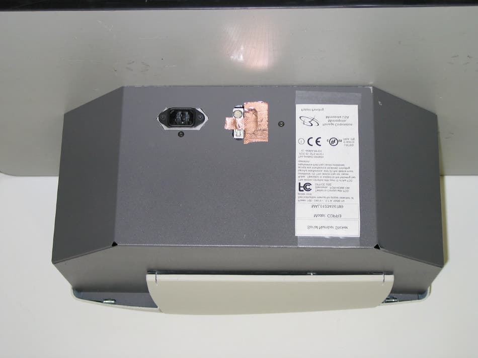
QT5-RFID1
Feb 18, 200313.56 MHz RFID Transceiver
Equipment Class
DXX - Part 15 Low Power Communication Device Transmitter