QTRPRS10001Print Server
Cellvision Systems Inc.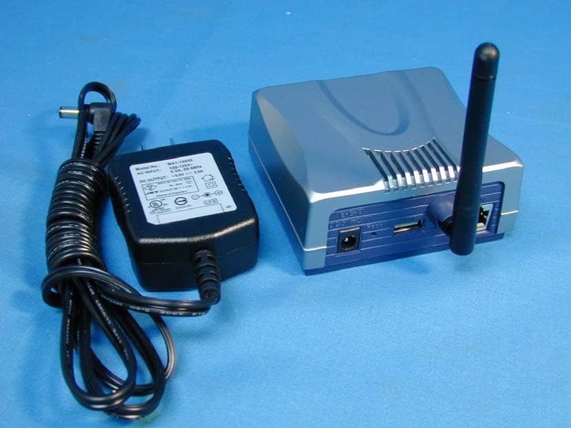
Click to zoom
Application Details
- Equipment Class
- DTS - Digital Transmission System
- Date of Grant
- May 26, 2003
- Application Purpose
- Original Equipment
- Date of Application
- May 26, 2003
- Equipment Note
- Print Server
- Frequency Range
- 2412.00000000 - 2462.00000000
- Company
- Cellvision Systems Inc.
- Country
- Taiwan
Documents & Files
Document Text
Text extracted from the exhibit documents filed with the FCC. Open a document above to read the original.
Users Manual
Wireless USB Print Server Quick Installation Guide Rev. 01 (February, 2003) Q20030101 Printed In Taiwan FCC Warning This device complies with Part 15 of the FCC Rules. Operation is subject to the following two conditions: (1) this device may not cause harmful interference, and (2) this device must accept any interference received, including interference that may cause undesired operation. CAUTION: Any Changes or modifications not expressly approved by the party responsible for compliance could void the authority to operate equipment. This equipment must be installed and operated in accordance with provided instructions and the antenna(s) used for this transmitter must be installed to provide a separation distance of at least 20 cm from all persons and must not be co-located or operating in conjunction with any other antenna or transmitter. End-users and installers must be provide with antenna installation instructions and transmitter operating conditions for satisfying RF exposure compliance. FCC Warning This equipment has been tested and found to comply with the regulations for a Class B digital device, pursuant to Part 15 of the FCC Rules. These limits are designed to provide reasonable protection against harmful interference when the equipment is operated in a commercial environment. This equipment generates, uses, and can radiate radio frequency energy and, if not installed and used in accordance with this user’s guide, may cause harmful interference to radio communications. Operation of this equipment in a residential area is likely to cause harmful interference, in which case the user will be required to correct the interference at his own expense. CE Mark Warning This is a Class B product. In a domestic environment, this product may cause radio interference, in which case the user may be required to take adequate measures. Table of Content Quick Installation Guide 1 Introduction 1 Unpacking 1 Port and LED Descriptions 2 Installing the Print Server 4 Installing and starting the PS Admin program 6 Installing PS Admin Program 6 Starting PS Admin Program 7 Configure Your Print Server 8 Choosing a Name for Your Print Server 8 Setting a Password for Your Print Server 9 Changing Print Server Port Settings 10 Setting up Workstation Printing 11 Windows 95/98/Me Client Workstation printing 11 Windows 2000/XP Client Workstation printing 12 Windows NT 4.0 Client Workstations Printing 13 Windows NT 3.51 Client Workstation Printing 14 Web Configuration of the Print Server 15 Appendix 16 Quick Installation Guide Introduction This Quick Installation Guide gives step-by-step instructions for setting up the print servers. The model you have purchased may appear slightly different from those shown in the illustrations. Examples in this manual are based on print servers. For more detailed information about the print server, its components, making network connections and technical specifications, please refer to the User’s Guide included with your print server. Unpacking Carefully remove all items from the package. In addition to this Quick Installation Guide, be certain that you have: ♦ One Wireless USB Print Server ♦ One AC Power adapter suitable for your country’s electric power service ♦ One Wireless USB Print Server Installation CD-ROM ♦ This Quick Installation Guide If any item is missing, or if you find any damage or mismatch, promptly contact your dealer for assistance. Port and LED Descriptions This section describes the visible parts of the print server. Front Panel There are three green LED indicators on the front panel: LEDs Description PW Steady light confirms that the Print Server is powered on. USB Steady blinking (briefly dark) is initiated when the printer is printing, otherwise, it remains dark. LAN Steady light confirms that the print server has a good connection to your network. When it blinks (briefly dark), the print server is receiving/ transmitting data from/to the network. WLAN Steady light confirms that the print server has a good connection to your wireless network. When it blinks (briefly dark), the print server is receiving/ transmitting data from/to the network. Back Panel Component Description DC Power Input The DC power input connector is located on the Print Server’s rear panel and is labeled DC 5V. Please note that the power supply included in the package is correct for this Wireless USB Print Server; substitution of other equipment may void warranty. Reset Button 1.) Press and release this button to reset the print server. 2.) Press and hold this button for three seconds (the USB LED on the front panel lights up) and then release it, the print server will resume the factory default settings. USB Port The USB port allows you connecting the print server to a printer with USB connector. Antenna To accept/transmit the data from/to your wireless network. LAN Connector This LAN connector (RJ-45) provides the printer server with connection to the network through 10/100 TX Ethernet cabling. The print server also supports web configuration permitting the users to configure settings through the web browser. Print Server’s default IP address as follows: ♦ Default IP address – 192.168.0.1 ♦ Subnet Mask – 255.255.255.0 Note: The PC’s IP address must correspond with the print server’s IP address in the same segment for the two devices to communicate. Installing the Print Server Follow these steps for a trouble-free start of print server operations with your Wireless USB Print Server. Please take particular notice that the network connection should be made before supplying power to the print server. WARNING: Configuration problems may result if the print server is powered up without first establishing its network connection. Please follow this procedure to avoid complications at the configuration stage. 1. Confirm proper operation of each of the printers to be connected to the print server. 2. When you have confirmed proper operation of the printer, switch its power off. 3. Confirm…
Text truncated - open the document above for the full version.
Block Diagram
Cellvision Systems Inc.3F-1, No.75, Hsin Taiwu Rd., Sec.1Hsichih, Taipei , Taiwan, R.O.C. Tel:886-2-26982562 Fax:886-2-26982565 Internet: [email protected] Parallel IC AT7601F CPU System RAM SDRAM(1M*16) System ROM Flash(256K*16) 100M PHY X'former CompactFlash Interface IEEE802.11b Wireless LAN Card Memory System LED (LAN status) Reset Button (factory reset) I/O Port Antenna RJ-45 LAN Switching adaptor 5V/2.4A Power System AC source Regulator 3.3V/5A Others 5V USB Wireless LAN Wire LAN PRS-201WU Block Diagram 3.3V USB USB Controller UBS connector (series A)
External Photos
Report No.: 033H014FI Page : 1 of 8 Version:1.0 Attachment 2 : EUT Detailed Photographs (1) EUT Photo (2) EUT Photo
ID Label/Location Info
Cellvision Systems Inc. FCC ID.: QTRPRS10001 FCC ID AND DoC Label The FCC ID and DoC Label will be placed on the equipment as shown in the photograph below. Print Server Model No.: PRS-201WU, WP-101U, TEW-PS1U, CP-810WU, S-PRS-201WU, C-PRS-201WU TESTED TO COMPLY WITH FCC STANDARDS FOR HOME OR OFFICE USE S/N: Made in Taiwan Print Server Model No.: PRS-201WU, WP-101U, TEW-PS1U, CP-810WU, S-PRS-201WU, C-PRS-201WU F F C C C C I I D D : : Q Q T T R R P P R R S S 1 1 0 0 0 0 0 0 1 1 This device complies with Part 15 of the FCC Rules. Operation is subject to the following two conditions: (1) this device may not cause harmful interference and (2) this device must accept any interference received, including interference that may cause undesired operation. S/N: Made in Taiwan
ID Label/Location Info
Cellvision Systems Inc. FCC ID.: QTRPRS10001 FCC ID AND DoC Label The FCC ID and DoC Label will be placed on the equipment as shown in the photograph below. Print Server Model No.: PRS-201WU, WP-101U, TEW-PS1U, CP-810WU, S-PRS-201WU, C-PRS-201WU TESTED TO COMPLY WITH FCC STANDARDS FOR HOME OR OFFICE USE S/N: Made in Taiwan Print Server Model No.: PRS-201WU, WP-101U, TEW-PS1U, CP-810WU, S-PRS-201WU, C-PRS-201WU F F C C C C I I D D : : Q Q T T R R P P R R S S 1 1 0 0 0 0 0 0 1 1 This device complies with Part 15 of the FCC Rules. Operation is subject to the following two conditions: (1) this device may not cause harmful interference and (2) this device must accept any interference received, including interference that may cause undesired operation. S/N: Made in Taiwan
Internal Photos
Report No.: 033H014FI Page : 2 of 8 Version:1.0 (3) EUT Photo (4) EUT Photo Report No.: 033H014FI Page : 3 of 8 Version:1.0 (5) EUT Photo Report No.: 033H014FI Page : 4 of 8 Version:1.0 (6) EUT Photo Report No.: 033H014FI Page : 5 of 8 Version:1.0 (7) EUT Photo (8) EUT Photo Report No.: 033H014FI Page : 6 of 8 Version:1.0 (9) EUT Photo Report No.: 033H014FI Page : 7 of 8 Version:1.0 (10) EUT Photo Report No.: 033H014FI Page : 8 of 8 Version:1.0 (11) EUT Photo (12) EUT Photo
Operational Description
Report No. 033H014FI Page: 5 of 34 Version:1.0 1.2. Operational Description EUT is a Print Server with 11 channels. This device provided four kind of transmitting speed 1,2,5.5 and 11Mbps. The device of RF carrier is DQPSK, DB PSK and CCK. The device adapts direct sequence spread spectrum modulation. The Connector antenna was provides diversity function to improve the receiving function. This Print Server is an IEEE 802.11b Wireless LAN adapter. It allows your computer to connect to a wireless network and to share resources, such as files or printers without being bound to the network wires. Operation in 2.4GHz Direst Sequence Spread Spectrum (DSSS) radio transmission, the Print Server transfers data at speeds up to 64/128-bit Wired Equivalent Protection (WEP) algorithm is used. In addition, its standard compliance ensures that it can communicate with any 802.11b network.
Schematics
5 5 4 4 3 3 2 2 1 1 DD CC BB AA Pin 39(PIO27) ID0= 0Software Version : 0.01UF*11(VDDIO,VDDC) Pin 38(/WR) = PU : ROM 16bitPin 116(TXD1_3/PDIVD1) = PU Pin 115(TXD1_2/PDIVD0) = PU Pin 114(TXD1_1/PFEREQ1) = PD Pin 112(TXD1_0/PFEREQ0) = PU 25MHZ*4=100MHZ Pin 117(TXEN1/CLKJMP)=PU : Multiple PLL enable 45657591991232359 97 18 Pin 33(ATPGEN)=PD : Sacn chain disable Pin 28(DTR1/SBWSEL)=PU : Slow bus disable Pin 32(JTAGEN)=PU : JTAGE enable CPU0A2 PRS-201WU Prepared : Peter Ku Issued Date: B 15Monday, January 20, 2003 Title SizeDocument NumberRev Date:Sheet of SW_RST /RD /WR ARDY /CIS/CIS /RD/WR /PCS5/PCS5 /RD/WR /OE /IORD /WE /IOWR /PCS2 /PCS3/REG WL_A9 /PCS2 A9 AD7 AD2 AD9 AD6 AD8 AD11 AD10 AD12 AD5 AD14 AD15 AD0 AD13 AD4 AD1 AD3 /PCS2 /PCS3 /PCS5 A15 A12 A13 A7 A9 A14 A5 A8 A4 A2 A6 A10 A1 A11 A3 /UCS INT0 A0 A[0..18] AD[0..15] WL_CD2 /CS_USB SW_RST INT2 /WL_LED MDIO MDC COL RXER RXDV RXC TXC RXD0RXD1RXD2RXD3 TXD[0..3] RXD[0..3] /RST_CPU /RST_CPU /SD_WE /SD_RAS DQML /SD_CAS SD_CLK DQMH PHYCHG TXD2 TXD1 TXD3 TXD0 PD1PQ0 TXEN PD0PQ1 RST/RSTRSTWL A17 A18 A16 /CIS /PCS5 ID0 /USB_LED ID1 /WL_CE2 RST 3.3V 3.3V 3.3V 3.3VP23.3VP2 3.3V 3.3V 3.3V 3.3V 3.3V 3.3V 3.3V 3.3V 3.3V 3.3V 3.3VP2 3.3V 3.3V 3.3V 3.3V 3.3V 3.3V 3.3V 3.3V 3.3V 3.3V 3.3V R12100 5% 1/16W R51330 5% 1/16W C39C38C46C52 R63 100 5% 1/16W U5C 74LVC32 9 10 8 14 7 U5B 74LVC32 4 5 6 14 7 C53 X2 X'TAL 25MHz U5D 74LVC32 12 13 11 14 7 C49 C33 20PF R62100 5% 1/16W R55330 5% 1/16W R48 100 5% 1/16W C50 R49 10K 5% 1/16W C47 0.1UF C34 0.1UF C42 C40 RA7100*4 5% 1/16W 1 2 3 4 8 7 6 5 R14100 5% 1/16W U5A 74LVC32 1 2 3 14 7 C60 R65 100 5% 1/16W R1510K 5% 1/16W R71 100 5% 1/16W R64 100 5% 1/16W R31 100 5% 1/16W U6A 74LVC08 1 2 3 14 7 U6B 74LVC08 4 5 6 14 7 C48 0.01UF U6D 74LVC08 12 13 11 14 7 R52100 5% 1/16W R53100 5% 1/16W C35 0.01UF U3B 74LVC14 34 RA6100*4 5% 1/16W 1 2 3 4 8 7 6 5 C24 47UF/25V C6 47UF/25V RA2100*4 5% 1/16W1 2 3 4 8 7 6 5 R5610K 5% 1/16W R23 100 5% 1/16W U3C 74LVC14 56 R61100 5% 1/16W R25100 5% 1/16W R26100 5% 1/16W R24100 5% 1/16W C13 0.01UF R6010K 5% 1/16W R5810K 5% 1/16W U4 R1610 128 127 10 12 11 13 8 6 26 25 17 20 85 84 82 86 126 125 34 35 124 95 94 93 92 90 89 88 87 61 60 58 57 56 54 53 52 79 78 77 76 71 70 69 68 80 66 51 50 49 48 47 44 43 96 100 72 67 46 9 14 120 5 16 15 37 38 122 18 1 4 64 74 32 33 39 41 42 45 65 75 91 99 123 36 55 73 81 98 113 23599712174083101636232 111117112114115116110102103109108107106118105104 19 21 22 24 27 28 29 30 31 119 X1 X2 TMRIN0 TMROUT0 TMROUT1 DRQ1/INT6 INT0 INT1/SELECT SOUT1 SIN1 RTS0/SAD9 CTS0/SAD8 WE CAS RAS DQML PCS0 PCS1 PCS2 PCS3 PCS5 AD0 AD1 AD2 AD3 AD4 AD5 AD6 AD7 AD8 AD9 AD10 AD11 AD12 AD13 AD14 AD15 A0/MA0 A1/MA1 A2//MA2 A3/MA3 A5/MA5 A6/MA6 A7/MA7 A8/MA8 A10/MA10 A11/SAD0 A12/SAD1 A13/SAD2 A14/SAD3 A15/SAD4 A16/SAD5 A18/SAD7 A19/ALE UCS CLKOUTA A4/MA4 A9/MA9 A17/SAD6 TMRIN1 DRQ0/INT5 RES INT2/INTA0/PWD SOUT0/SAD13 SIN0/SAD14 RD WR/BWSEL ARDY VDDIO VSSIO NMI DQMH SD_CLK JTAGEN ATPGEN PIO27 PIO28 PIO29 VDDIO VDDIO VDDIO VDDIO VDDIO VDDIO VSSIO VSSIO VSSIO VSSIO VSSIO VSSIO VDDCVDDCVDDCVDDCVSSCVSSCVSSCVSSCVDDP1VSSP1VDDP2VSSP2 TXC1 TXEN1/CLKJMP TXD1_0/PFEREQ0TXD1_1/PFEREQ1 TXD1_2/PDIVD0TXD1_3/PDIVD1 RXC1 MDIO1 MDC1 RXD1_3RXD1_2RXD1_1RXD1_0 COL1 RXDV1RXER1 DTR0/SAD12 DSR0/SAD11 DCD0/SAD15 RI0/SAD10 RTS1/TD0 DTR1/SBWSEL CTS1/TMS DSR1/TCK DCD1/TDI PHY_CHG1 R591K 5% 1/16W RA347*4 5% 1/16W1 2 3 4 8 7 6 5 U3D 74LVC14 98 U6C 74LVC08 9 10 8 14 7 R20100 5% 1/16W R45100 5% 1/16W R9100 5% 1/16W R6 10K 5% 1/16W R10100 5% 1/16W C21 0.01UF R775 5% 1/16W R875 5% 1/16W RA8100*4 5% 1/16W1 2 3 4 8 7 6 5 R57 10K 5% 1/16W R22100 5% 1/16W R7275 5% 1/16W R50 330 5% 1/16W RA1047*4 5% 1/16W 1 2 3 4 8 7 6 5 RA5 100*4 5% 1/16W 1 2 3 4 8 7 6 5 RA947*4 5% 1/16W 1 2 3 4 8 7 6 5 Q2 XC61FC3012MR XC61B 31 2 VINVOUT VSS R46 100K 1% 1/16W C36 0.1UF C44 0.01UF SW1 PUSH BOTTON C43 10UF/10V R47 1M 5% 1/16W L8 BEAD 1206 C41 20PF RA447*4 5% 1/16W 1 2 3 4 8 7 6 5 R5410K 5% 1/16W C8 0.01UF U3A 74LVC14 12 RA1100*4 5% 1/16W 1 2 3 4 8 7 6 5 /OE(5) /IORD(5) /WE(5) /IOWR(5) /REG(5) WL_A9(5) SD_CLK(2) /UCS(2) INT0(5) WL_CD2(5) INT2(4) /WL_LED(4) AD[0..15](2,4,5) A[0..18](2,4,5) TXD[0..3](3) RXD[0..3](3) TXC(3) RXC(3) RXDV(3) RXER(3) COL(3) MDIO(3) MDC(3) ARDY(5) /RD(2,4) /WR(2,4) WL_CD1(5) /SD_RAS(2) /SD_WE(2) DQML(2) /SD_CAS(2) DQMH(2) PHYCHG(3) TXEN(3) /RST(3,4) RSTWL(5) /CS_USB(4) /USB_LED(4) /WL_CE2(5) 5 5 4 4 3 3 2 2 1 1 DD CC BB AA 0.01UF*2 0.01UF*4 125 7133844 37 0A2 PRS-201WU Prepared: Peter Ku Issued Date: B 25Monday, January 20, 2003 Memory Title SizeDocument NumberRev Date:Sheet of AD3 A1 /RD A3 A11 AD6 AD4 AD5 AD7 A6 AD10 A17 A15 AD1 AD14 A4 A18 A9 A12 AD0 AD9 AD11 A8 AD12 A13 A14 A16 A7 AD13 A5 AD2 A2 AD15 A10 AD8 /UCS /WR SD_CLK /SD_WE /SD_CAS DQML DQMH /SD_RAS AD8 AD9 AD10 AD11 AD12 AD13 AD14 AD15 A0 A1 A2 A3 A5 A4 A6 A7 A8 A10 A9 AD[0..15] A[0..18] AD6 AD5 AD1 AD2 AD7 AD3 AD4 AD0 3.3V 3.3V3.3V 3.3V 3.3V 3.3V 3.3V 3.3V 3.3V 3.3V RA1347*4 5% 1/16W 1 2 3 4 8 7 6 5 RA1547*4 5% 1/16W 1 2 3 4 8 7 6 5 C61C56 C23 0.01UF U7 29LV400-TSOP 29F400-TSOP 1 2 3 4 5 6 7 8 9 10 11 12 13 14 15 16 17 18 19 20 21 22 23 24 48 47 46 45 44 43 42 41 40 39 38 37 36 35 34 33 32 31 30 29 28 27 26 25 A15 A14 A13 A12 A11 A10 A9 A8 NC NC /WE /RESET NC NC RY/BY NC A17 A7 A6 A5 A4 A3 A2 A1 A16 /BYTE VSS DQ15 DQ7 DQ14 DQ6 DQ13 DQ5 DQ12 DQ4 VCC DQ11 DQ3 DQ10 DQ2 DQ9 DQ1 DQ8 DQ0 /OE VSS /CE A0 C58 RA1447*4 5% 1/16W 1 2 3 4 8 7 6 5 RA1247*4 5% 1/16W 1 2 3 4 8 7 6 5 U9 KM416S1120D 2 3 5 6 8 9 11 12 39 40 42 43 45 46 48 49 1 50 7 13 38 44 4 10 41 47 34 35 21 22 23 24 27 28 29 30 31 32 20 25 26 18 19 17 16 15 14 36 33 37 DQ0 DQ1 DQ2 DQ3 DQ4 DQ5 DQ6 DQ7 DQ8 DQ9 DQ10 DQ11 DQ12 DQ13 DQ14 DQ15 VDD VSS VDDQ VDDQ VDDQ VDDQ VSSQ VSSQ VSSQ VSSQ CKE CLK A0 A1 A2 A3 A4 A5 A6 A7 A8 A9 A10/AP VDD VSS CS BA RAS CAS WE LDQM UDQM NC NC/RFU C63 10UF/10V C20 10UF/10V C18 10UF/10V C66 10UF/10V C67 C59 C62 A[0..18](1) AD[0..15](1,4,5) /WR(1) /RD(1) /UCS(1) SD_CLK(1) /SD_RAS(1) /SD_CAS(1) /SD_WE(1) DQML(1) DQMH(1) 5 5 4 4 3 3 2 2 1 1 DD CC BB AA 0603 0.01UF*4 2413 31474238 7 0.01UF*…
Text truncated - open the document above for the full version.
Test Report
Report No. 033H014FI Page: 1 of 34 Version:1.0 Test Report Product Name : Print Server Model No.: PRS-201WU, WP-101U, TEW-PS1U, CP-810WU, S-PRS-201WU, C-PRS-201WU FCC ID.: QTRPRS10001 Applicant : Cellvision Systems Inc. Address : 18F-7, No. 79, Sec. 1, Hsin Taiwu Road, Hsichih, Taipei, Taiwan, R.O.C. Date of Receipt : Mar 05, 2003 Date of Test : Apr 25, 2003 Report No. : 033H014FI The test results relate only to the samples tested. The test report shall not be reproduced except in full without the written approval of QuieTek Corporation. This report must not be used to claim product endorsement by NVLAP any agency of the U.S. Government Report No. 033H014FI Page: 2 of 34 Version:1.0 Test Report Certification Test Date : Apr 25, 2003 Report No. : 033H014FI The Test Results relate only to the samples tested. The test report shall not be reproduced except in full without the written approval of QuieTek Corporation. This report must not be used to claim product endorsement by NVLAP any agency of the U.S. Government Product Name : Print Server Applicant : Cellvision Systems Inc. Address : 18F-7, No. 79, Sec. 1, Hsin Taiwu Road, Hsichih, Taipei, Taiwan, R.O.C. Manufacturer : Cellvision Systems Inc. Model No. : PRS-201WU, WP-101U, TEW-PS1U, CP-810WU, S-PRS-201WU, C-PRS-201WU FCC ID. : QTRPRS10001 Rated Voltage : AC 120V/60Hz Trade Name : Non-Brand Measurement Standard : FCC Part 15 Subpart C Paragraph 15.247 Measurement Procedure : ANSI C63.4: 1992 Test Result : Complied Documented By : ( Carol Tasi ) Tested By : ( Ken Hsu ) Approved By : ( Kevin Wang ) Accredited by NIST (NVLAP) NVLAP Lab Code: 200347-0 Report No. 033H014FI Page: 3 of 34 Version:1.0 TABLE OF CONTENTS Description Page 1. GENERAL INFORMATION .....................................................................................................4 1.1. EUT Description............................................................................................................................4 1.2. Operational Description ................................................................................................................5 1.3. Tested System Datails....................................................................................................................6 1.4. Configuration of tested System .....................................................................................................7 1.5. EUT Exercise Software .................................................................................................................7 1.6. Test Facility ...................................................................................................................................8 2. Conducted Emission....................................................................................................................9 2.1. Test Equipment..............................................................................................................................9 2.2. Test Setup ......................................................................................................................................9 2.3. Limits ............................................................................................................................................9 2.4. Test Procedure .............................................................................................................................10 2.5. Test Result of Conducted Emission.............................................................................................11 3. Peak Power Output ...................................................................................................................13 3.1. Test Equipment............................................................................................................................13 3.2. Test Setup ....................................................................................................................................13 3.3. Limits ..........................................................................................................................................13 3.4. Test Result of Peak Power Output...............................................................................................14 4. Radiated Emission .....................................................................................................................15 4.1. Test Equipment............................................................................................................................15 4.2. Test Setup ....................................................................................................................................15 4.3. Limits ..........................................................................................................................................16 4.4. Test Procedure .............................................................................................................................17 4.5. Test Result of Radiated Emission................................................................................................18 5. Band Edge ..................................................................................................................................24 5.1. Test Equipment............................................................................................................................24 5.2. Test Setup ....................................................................................................................................24 5.3. Limits ..........................................................................................................................................25 5.4. Test Procedure .............................................................................................................................25 5.5. Test Result of Band Edge ......................................................…
Text truncated - open the document above for the full version.
Test Setup Photos
Report No.: 033H014FI Page : 1 of 3 Version:1.0 Attachment 1: EUT Test Setup Photographs Front View of Conducted Test Back View of Conducted Test Report No.: 033H014FI Page : 2 of 3 Version:1.0 Front View of Radiated Test Back View of Radiated Test Report No.: 033H014FI Page : 3 of 3 Version:1.0 Front View of Radiated Test (Horn)
Contact Information
Applicant
Celia Chu(Specialist)
Test Firm
DEKRA Testing and Certification Co., Ltd.Sky Hsu
Technical Specifications
| # | Rule Parts | Frequency Range | Power Output |
|---|---|---|---|
| 1 | 15C | 2.41 GHz - 2.46 GHz | 28.00 mW |
Other Applications from Cellvision Systems Inc.
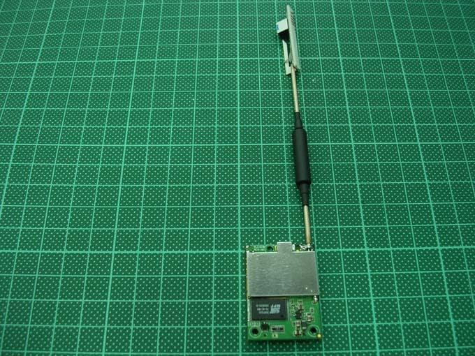
QTRWLC10002
Nov 09, 2003Mini-ISA 2.4 GHz 802.11 Card
Equipment Class
DTS - Digital Transmission System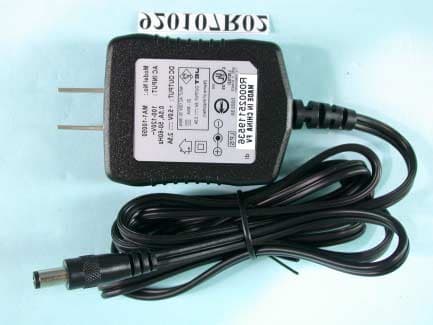
QTRWBA10001
Jul 28, 2003Bridge AP / Repeater AP
Equipment Class
DTS - Digital Transmission System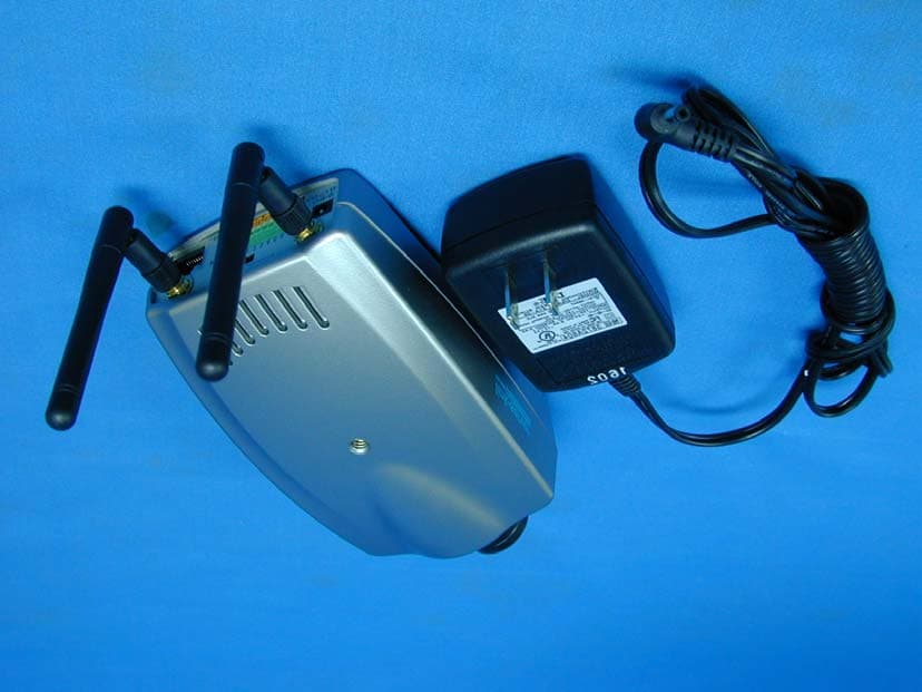
QTRCAS10001
Mar 10, 2003Wireless Internet Camera
Equipment Class
DTS - Digital Transmission System