R55KSM60102 Way FRS & GMRS Micro-Wristband Communicators
Kids Station Toys Incorporated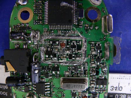
Click to zoom
Application Details
- Equipment Class
- FRF - Part 95 Family Radio Face Held Transmitter
- Date of Grant
- Mar 30, 2005
- Application Purpose
- Original Equipment
- Date of Application
- Mar 30, 2005
- Equipment Note
- 2 Way FRS & GMRS Micro-Wristband Communicators
- Frequency Range
- 462.55000000 - 462.72500000
- Country
- Hong Kong
Documents & Files
Document Text
Text extracted from the exhibit documents filed with the FCC. Open a document above to read the original.
Users Manual
Model: KSM6010 PLEASE READ BEFORE OPERATING THIS EQUIPMENT. 1 Two-Way FRS/GMRS Micro-Wristband Communicators with Neckband and Belt Clip OWER'S MANUALN 1 SAFETY PRECAUTIONS Safety and General Information Exposure to Radio Frequency Energy Your radio is designed to comply with the following national and international standards and guidelines regarding exposure of human beings to radio frequency electromagnetic energy: • United States Federal Communications Commission, Code of Federal Regulations; 47 CFR part 2 sub-part J • American National Standards Institute (ANSI)/Institute of Electrical and Electronic Engineers (IEEE) C95.1-1992 • Institute of Electrical and Electronic Engineers (IEEE) C95.1-1999 Edition Safety and General Information 4 • International Commission on Non-Ionizing Radiation Protection (ICNIRP) 1998 •Ministry of Health (Canada) Safety Code 6. Limits of Human Exposure to Radio Frequency Electromagnetic Fields in the Frequency Range from 3 kHz to 300GHz, 1999 •Australian Communications Authority Radiocommunications (Electromagnetic Radiation–Human Exposure) Standard 2001 (applicable to wireless phones only) • ANATEL, Brazil Regulatory Authority, Resolution 256 (April 11, 2002) “additional requirements for SMR, cellular, and PCS product certification.” To assure optimal radio performance and make sure human exposure to radio frequency electromagnetic energy is within the guidelines set forth in the above standards, always adhere to the following procedures. Portable Radio Operation and EME Exposure Antenna Care Use only the supplied or an approved replacement antenna. Unauthorized antennas, modifications or attachments could damage the radio and may violate FCC regulations. DO NOT hold the antenna when the radio is “IN USE.” Holding the antenna affects the effective range. Two-Way Radio Operation When using your radio as a traditional two-way radio, hold the radio in a vertical position with the microphone 2 to 3 inches away from the lips. 2 Electromagnetic Interference/Compatibility NOTE:Nearly every electronic device is susceptible to electromagnetic interference (EMI) if inadequately shielded, designed or otherwise configured for electromagnetic compatibility. Facilities To avoid electromagnetic interference and/or compatibility conflicts, turn off your radio in any facility where posted notices instruct you to do so. Hospitals or health care facilities may be using equipment that is sensitive to external RF energy. Aircraft When instructed to do so, turn off your radio when on board an aircraft. Any use of a radio must be in accordance with applicable regulations per airline crew instructions. Medical Devices Pacemakers The Advanced Medical Technology Association recommends that a minimum separation of 6 inches (15 centimeters) be maintained between a handheld wireless radio and a pacemaker. These recommendations are consistent with the independent research by, and recommendations of, the U.S. Food and Drug Administration. Persons with pacemakers should: •ALWAYS keep the radio more than six inches (15 centimeters) from their pacemaker when the radio is turned ON. •not carry the radio in the breast pocket. •use the ear opposite the pacemaker to minimize the potential for interference. • turn the radio OFF immediately if you have any reason to suspect that interference is taking place. SAFETY PRECAUTIONS WARNING USE UNDER SUPERVISION OF AN ADULT DUE TO LONG CORD. This unit has a long AC cord or other long cord that can easily be tripped on or pulled on, causing injury. Please make sure it is arranged so it will not drape over a tabletop, etc. where it can be pulled on by children or tripped over accidentally. EXERCISE CAUTION AS UNIT HAS SHARP POINTS. 1 2 3 5 4 6 10 7 8 9 11 12 1. MENU Button 2. Antenna 3. Display 4. POWER Button 5. TALK Button 6. UP Button 7. Speaker 8. Wrist Strap 9. CALL Button 10. Microphone 11. Handsfree Jack 12. DOWN Button 13. Channel Number 14. DM (Dual Watch) 15. VX (Voice Activated) 16. SC (Scan All) 17. Lock 18. Battery Level 19. TX (Transmit) 20. RX (Receive) 21. Volume Level 22. Call Tone 23. Timer 24. Subchannel Number LOCATION OF CONTROLS UNIT B T T DM VX SC V O L TX RX 14 15 17 16 18 13 19 20 22 23 24 21 DISPLAY INSTALLATION 4 BATTERY PRECAUTIONS Follow these precautions when using batteries in this device: 1. Use only the size and type of batteries specified. 2. Be sure to follow the correct polarity when installing the batteries as indicated in the battery compartment. Reversed batteries may cause damage to the device. 3. Do not mix different types of batteries together (e.g. Alkaline, rechargeable and Carbon-zinc) or old batteries with fresh ones. 4. If the device is not to be used for a long period of time, remove the batteries to prevent damage or injury from possible battery leakage. 5. Do not try to recharge batteries not intended to be recharged; they can overheat and rupture. (Follow battery manufacturer’s directions.) Remove the screw, then lift off the battery cover. 1 Insert three (3) AAA batteries as shown by the polarity diagram in the compartment. Replace the battery cover. 2 REPLACING THE BATTERIES INSTALLATION (CONTINUED) 5 Insert the unit onto the belt base and slide until it locks into the base. 1 To remove the unit from the Belt base, press both latches to unlock the unit from the base and slide it out. 2 USING THE WRIST STRAP Press the latch and remove the string from the necklace. Insert the string into the neck strap hole and tie it. 1 Connect the string part into the main strap. 2 USING THE NECK STRAP INSTALLATION (CONTINUED) 6 NECKLACE BTT DM V X SC VOL TX RX TALK 1 HANDS-FREE (VOX) BTT DM VX SC VOL TX RX TALK 3 WRISTWATCH The watch can be rotated as desired. BTT DM VX SC VOL TX RX TALK BTT DMVXSC V OL TX RX TALK 2 HOW TO WEAR OPERATION 7 While in the Watch mode, press and hold the MENU button for three seconds; the hours will blink. 1 Press the UP 1or DOWN 2 button to set the present hour, then press the MENU butt…
Text truncated - open the document above for the full version.
Block Diagram
FX95 frs BLK.SCH-1 - Wed Mar 09 09:50:56 2005
ID Label/Location Info
APPENDIX A - FCC ID LABELING AND LOCATION Proposed FCC ID Labeling Proposed FCC ID Location Bottom View of EUT / Proposed Label Location Labeling Requirement Each equipment for which a type acceptance applications is filed on or after May 1, 1981, shall bear an identification plate or label pursuant to §2.295 (Identification of Equipment) and §2.926 (FCC identifier) In August 1996 the Federal Communications Commissions (FCC) adopted RF exposure guidelines with safety levels for hand-held wireless devices. Generally users manual contains a RF exposure statement to indicate compliance with FCC requirements. The users manual should also contain required information and instruction pursuant to 95.653. FCC ID: R55KSM6010
Internal Photos
EUT – Board and Housing View EUT – Component View EUT – Solder View EUT – Solder View Shield off View
Operational Description
- 1 - CIRCUIT DESCRIPTION 1. RECEIVER SECTION Radio Frequency signal received by the antenna (ANT1), passing through the Low Pass Filter (L1,L18, C31,C165,C191). The RF signal is then amplified by Low Noise Amplifier Q26 and passes through a Band Pass Filter of FL1. The filtered signal within the range of 462 MHz – 467 MHz is then mixed with the first local oscillator signal from the Voltage Controlled Oscillator (VCO) circuit (Q29,Q31, D11, L24) through Q27, a portion of VCO signal is then feedback to the PLL IC (IC9) for phase comparison generating a stable RX frequency, the output signal is filtered by FL3 (21.7 MHz) which is the first Intermediate Frequency (IF) . The IF signal is fed to the discriminator IC9 pin 41 which is then mixed with the second local oscillator supplied by crystal X2 (21.25 MHz) to produced a reduced second IF signal which is then filtered by FL2 (LTM450HTU). Demodulated signal is recovered through correct and the internal discriminator circuit of IC9. The recovered Audio signal is outputted at pin 26 of IC9, the fully recovered audio signal is then further amplified by Power Amplifier IC5. An audible sound is therefore produce by the speaker SPK1. 2. TRANSMITTER SECTION PTT switch (SW19) when pushed triggers the Transmitter Circuit “ON”, the voice signal generates by the surrounding noise passes through the microphone MIC1 where mechanical to electrical transformation occurs, the electrical transformed signal is then filtered by Q40. The output signal is Modulated by a modulator circuit with a varactor diode D11 and L24. The external components from Q31,Q29 form a VCO Circuit which generates the required oscillating frequency for transmission, a portion of this signal is feedback to the PLL IC9 pin 46 for phase comparison in order to produce a stabilized TX frequency. The modulated signal is then amplified by a Cascaded Amplifier Circuit Q28 and 32 and again amplified by Q42 to produce a sufficient Radio Frequency signal emitted by the Antenna (ANT1). 3. CALL TRANSMISSION By pushing the CALL key, a signal is detected by the CPU (IC4), a CALL data is then produced by the CPU. This data passes through the Low Pass Filter Q40 and modulated by the varactor diode D11 and L24. The signal follows it’s conventional transmission section path through the antenna. 4. BATTERY LOW DETECTION - 2 - Battery Low Detection is controlled by the CPU pin 36 as detected on the LCD 1, however a voltage divider circuit R173,174 and R184 serve as the stabilize reference voltage for the CPU to process its detection. 5. SQUELCH DETECTION Supported by the linear IC circuit (IC9), a resistor R216 sets the level of detection as a comparator circuit interface with the CPU. 6. POWER SUPPLY Supply voltage of 3.8 Volts dc is needed to power “ON” the whole circuitry, by Lithium Ion Rechargeable battery pack. 7. Battery Charging Battery Charging by DC adaptor through the ear jack and CPU pin 6 monitoring the charging status and once its fully charged the Q37 turn off to stop the charge to protect battery from its over charge. FREQUENCY CHART CHANNEL FREQUENCY (MHz) CHANNEL FREQUENCY (MHz) 1 462.5625 12 467.6625 2 462.5875 13 467.6875 3 462.6125 14 467.7125 4 462.6375 15 462.5500 5 462.6625 16 462.5750 6 462.6875 17 462.6000 7 462.7125 18 462.6250 8 467.5625 19 462.6500 9 467.5875 20 462.6750 10 467.6125 21 462.7000 11 467.6375 22 462.7250
Operational Description
ALIGNMENT PROCEDURE AND SPECIFICATION A. STANDARD TEST CONDITION 1. RF IN/OUT IMPEDANCE ----- 50 OHM 2. RF SIGNAL GENERATOR RF OUTPUT ----- -47dBm MODULATION ----- 1 Khz, 0.5 Khz DEVIATION 3. SPEAKER OUTPUT IMPEDANCE ----- 16 OHM 4. SPEAKER VOLUME ----- MAXIMUM 5. MIC INPUT SIGNAL ----- 1 Khz 10 mVrms 6. POWER SUPPLY ----- DC 4.5V +/- 15% B. ELECTRICAL TEST ITEMS 1. VCO VOLTAGE ADJUSTMENT 1) PRESS AND HOLD DOWN THE POWER BUTTON TO POWER ON 2) PRESS THE TALK BUTTON INTO THE TX MODE 3) CONNECT THE DC VOLT METER TO TP1 4) ADJUST L18 AND OBSERVE DC VOLTAGE LIMIT : 0.8 +/- 0.3 Vdc 2. FREQUENCY ADJUSTMENT 1) CONNECT THE FREQUENCY COUNTER TO ANT POINT 2) PRESS THE TALK BUTTON 3) ADJUST THE FREQUENCY BY CV1 LIMIT : +/- 100 Hz 3. TX POWER CHECK 1) CONNECT THE RF POWER METER TO ANT POINT 2) PRESS THE TALK BUTTON 3) MEASURE THE TX POWER LIMIT : 25dBm +/- 1 dB Measured:22.67dBm(Conducted) Measured:11.16dBm(ERP) 4. MIC MODULATION SENSITIVITY CHECK 1) CONNECT THE MODULATION METER TO ANT. 2) THE AUDIO SIGNAL INPUT TO MIC. 3) PRESS THE TALK BUTTON 4) MEASURE THE MODULATE DEV. LIMIT : 0.9 +/- 0.3 Khz DEV . 5. MAXIMUM DEVIATION CHECK 1) CONNECT THE MODULATION METER TO ANT. 2) THE AUDIO SIGNAL INPUT TO MIC. 3) INCREASE THE AUDIO LEVEL BY 20DB 4) PRESS THE TALK BUTTON 5) MEASURE THE MODULATE DEV. LIMIT : 1.9 +/- 0.4 Khz DEV . 6. CALL SIGNAL MODULATION DEV. CHECK 1) CONNECT THE MODULATION METER TO ANT. 2) PRESS THE CALL BUTTON 3) MEASURE MODULATE DEV. LIMIT : 1.2 +/- 0.3 Khz DEV. 7. LOW BATTERY DETECT CHECK 1) VARY THE DC POWER 2) OBSERVE THE BATTERY ICON INSIDE BARS DISAPPEARED 3) MEASURE THE DC POWER VOLTAGE LIMIT : 3.5 +/- 0.1 Vdc 8. ESCRIMINATOR ADJUST 1) CONNECT THE SSG TO ANT. 2) CONNECT THE DC VOLT METER TO TP10 3) MEASURE TP10 VOLTAGE LIMIT : 1.3 +/- 0.2 Vdc 9. SPEAKER OUTPUT LEVEL CHECK 1) CONNECT THE SSG TO ANT. 2) CONNECT THE AUDIO VOLT METER TO SPK. 3) MEASURE THE SPEAKER OUTPUT LEVEL LIMIT : -1 +/- 4 dBm 10. RECEIVING SENSITIVITY CHECK 1) CONNECT THE SSG TO ANT. 2) CONNECT THE SINAD METER TO SPK. 3) REDUCE THE SSG RF OUT PUT LEVEL UP TO SINAD 12dB 4) MEASURE THE SSG RF OUTPUT LEVEL LIMIT : < -116 dBm 11. SQ CHECK 1) CONNECT THE SSG TO ANT. 2) CONNECT THE SINAD METER TO SPK. 3) CONNECT THE DC VOLT METER TO TP12 4) REDUCE THE SSG RF OUTPUT UP TO TP12 IS CHATERING 5) MEASURE THE SINAD METER LIMIT : 6 +/- 2 dB
Parts List/Tune Up Info
ᅝᙺ⬉ᄤ ᅝᙺ⬉ᄤ ᅝᙺ⬉ᄤ ᅝᙺ⬉ᄤ ( ⏅ഇ ⏅ഇ ⏅ഇ ⏅ഇ ) ᳝䰤݀ৌ ᳝䰤݀ৌ ᳝䰤݀ৌ ᳝䰤݀ৌ ѻ ѻ ѻ ѻક ક ક ક㒧 㒧 㒧 㒧ᵘ ᵘ ᵘ ᵘ (Bill Of Material) Џӊ㓪ো Џӊ㓪ো Џӊ㓪ো Џӊ㓪ো : ARF-0003-112A Џӊৡ鹵 : PCBA_BM35 PANENT UNIT RF PCB ᴀऩԡ :PCS ᴎൟ ᴎൟ ᴎൟ ᴎൟ : BM35(RF) SMT PCB ASS PAK Џ⠜ᴀো :A2 ᔧࠡ⠜ᴀো : 00006 ব᮹ᳳ : 2004-11-2 15:21:27 বऩো : ECO04-0532 ᑣো ᭭ક㓪ো ᭭કৡ鹵 ⫼䞣 ԡ 㕂 ᤳ㗫⥛ 1 ARF-0003-112S SMT_RF FOR FX-10PMRV2(S300) BINATONE 1 2 ECC-6300-100A CAP_C_TRIMMER 10PF 1 CV1 3 EFT-1420-001A CRYSTAL FILTERS ET21.7MHz 1 FL2 4 EFT-5720-002A SAW_FILTERS HDF446A 50 /0PF 1 FL1 5 EPN-1131-001A CONNECTOR_13P PITCH2.0 15mm(3-3) 1 6 EPN-2021-003A HEADER_2P 2.0mm/H (14mm) 1 7 EWR-0280-444A WIRE 28mm/BLACK (4-4) AWG#22 1 8 EXR-1420-006A XTAL_21.250MHz(18PF)HC-49S(3.6mm)+/-3PPM(-20~+ 6 1 X1 9 MFB-0100-041A INSULATION PAPER (4.8+D2.95X2)X4.2X1.0mm 1 X1 10 MMT-0500-012A SHIELD COVER 19X17X3mm TIN-0.3T 1 11 MMT-0500-081A SHEET COPPER 10X8X0.1mm 1 12 MMT-0500-082A SHEET COPPER 28X15X0.1mm 1 13 MMT-0500-091A SHIELD COVER 11X11X2mm TIN-0.3T 1 14 MMT-0500-101A SHIELD COVER 19X14X2.3mm TIN-0.3T 1 15 MMT-0500-171A SHIELD COVER 14.5X(13.5x12)X1.6mm TIN-0.3T 1 16 MRB-0600-181A CUSHION 38X19X2mm(EVA) BLACK 1 17 MRB-0600-672A CUSHION 8X5X1mm (EVA) 1 FL2 ߫ॄᯊ䯈 : 2005-3-7 14:19:49 1/1 义 㸼ࠊ : 㕢⦆ ᅵḌ :____________________ ᅵᡍ :____________________ ޚᡍ :_____________________ ᅝᙺ⬉ᄤ ᅝᙺ⬉ᄤ ᅝᙺ⬉ᄤ ᅝᙺ⬉ᄤ ( ⏅ഇ ⏅ഇ ⏅ഇ ⏅ഇ ) ᳝䰤݀ৌ ᳝䰤݀ৌ ᳝䰤݀ৌ ᳝䰤݀ৌ ѻ ѻ ѻ ѻક ક ક ક㒧 㒧 㒧 㒧ᵘ ᵘ ᵘ ᵘ (Bill Of Material) Џӊ㓪ো Џӊ㓪ো Џӊ㓪ো Џӊ㓪ো : ARF-0003-112S Џӊৡ鹵 : SMT_BM35 PANENT UNIT RF PCB ᴀऩԡ :PCS ᴎൟ ᴎൟ ᴎൟ ᴎൟ :BM35(RF) SMT PCB ASS PAK Џ⠜ᴀো :A2 ᔧࠡ⠜ᴀো : 00007 ব᮹ᳳ : 2005-1-5 15:52:18 বऩো : ECO05-0009 ᑣো ᭭ક㓪ো ᭭કৡ鹵 ⫼䞣 ԡ 㕂 ᤳ㗫⥛ 1 BRF-B081-402C GTCHA RF RF-4-1.0T_4LAYER FX-10(RF:03) 1 PCB_RF 2 ECS-1212-010B CAP_C_CHIP 1PF/C(CH)(0603) A:COG150L (SAMSUN G 1 C37 3 ECS-1212-020B CAP_C_CHIP 2PF/C(CH)(0603) A:COG150L (SAMSUN G 3 C41,C70,C71 4 ECS-1212-030B CAP_C_CHIP 3PF/C(CH)(0603) A:COG150L (SAMSUN G 3 C9,C51,C13 5 ECS-1212-040B CAP_C_CHIP 4PF/C(CH)(0603) A:COG150L (SAMSUN G 2 C44,C49 6 ECS-1212-050B CAP_C_CHIP 5PF/C(CH)(0603) A:COG150L (SAMSUN G 5 C2,C20,C43,C47,C38 7 ECS-1213-060B CAP_C_CHIP 6PF/D(CH)(0603) A:COG150L (SAMSUN G 3 C21,C11,C31 8 ECS-1213-070B CAP_C_CHIP 7PF/D(CH)(0603) A:COG150L(SAMSUNG ) 2 C46,C33 9 ECS-1213-080B CAP_C_CHIP 8PF/D(CH)(0603) A:COG150L(SAMSUNG ) 1 C8 10 ECS-1213-090B CAP_C_CHIP 9PF/D(CH)(0603) A:COG150L (SAMSUN G 2 C73,C45 11 ECS-1213-100B CAP_C_CHIP 10PF/D/(CH)/(0603) A:COG150L (SAMSU N 5 C14,C15,C32,C42,C54 12 ECS-1216-101B CAP_C_CHIP 100PF/J(CH)(0603) A:COG150L (SAMSU N 4 C22,C28,C35,C60 13 ECS-1216-120B CAP_C_CHIP 12PF/J(CH)(0603) A:COG150L (SAMSUN G 1 C5 14 ECS-1216-150B CAP_C_CHIP 15PF/J(CH)(0603) A:COG150L (SAMSUN G 2 C3,C36 15 ECS-1216-180B CAP_C_CHIP 18PF/J(CH)(0603) A:COG150L (SAMSUN G 1 C23 16 ECS-1216-200B CAP_C_CHIP 20PF/J(CH)(0603) A:COG150L (SAMSUN G 1 C61 17 ECS-1216-220B CAP_C_CHIP 22PF/J(CH)(0603) A:COG150L (SAMSUN G 2 C19,C12 18 ECS-1216-221B CAP_C_CHIP 220PF/J(CH)(0603) A:COG150L (SAMSU N 2 C48,C64 19 ECS-1216-820B CAP_C_CHIP 82PF/J(CH)(0603) A:COG150L (SAMSUN G 2 C58,C59 20 ECS-2296-471B CAP_C_C.H.D. B470PF/J(0603) X:X7R282L (SAMSUNG ) 1 C1 21 ECS-2297-102B CAP_C_C.H.D. B0.001uF/K(0603) X:X7R282L (SAMSUN 3 C26,C57,C62 22 ECS-2297-103A CAP_C_C.H.D. B0.01uF/K(0603) X:X7R282L 5 C17,C27,C52,C68,C69 23 ECS-2297-333A CAP_C_C.H.D. B0.033uF/K(0603) X:X7R282L 1 C4 24 ECS-2297-471B CAP_C_C.H.D. B470PF/K(0603) X:X7R282L(SAMSUNG ) 6 C7,C18,C29,C34,C40,C53 25 ECS-2297-473A CAP_C_C.H.D. B0.047uF/K(0603) X:X7R282L 1 C65 26 ECS-22A8-104A CAP_C_C.H.D. F0.1uF/M(0603) Y:YF153L 4 C24,C25,C56,C66 ߫ॄᯊ䯈 : 2005-3-7 14:19:50 1/3 义 㸼ࠊ : 㕢⦆ ᅵḌ :____________________ ᅵᡍ :____________________ ޚᡍ :_____________________ ᅝᙺ⬉ᄤ ᅝᙺ⬉ᄤ ᅝᙺ⬉ᄤ ᅝᙺ⬉ᄤ ( ⏅ഇ ⏅ഇ ⏅ഇ ⏅ഇ ) ᳝䰤݀ৌ ᳝䰤݀ৌ ᳝䰤݀ৌ ᳝䰤݀ৌ ѻ ѻ ѻ ѻક ક ક ક㒧 㒧 㒧 㒧ᵘ ᵘ ᵘ ᵘ (Bill Of Material) Џӊ㓪ো Џӊ㓪ো Џӊ㓪ো Џӊ㓪ো : ARF-0003-112S Џӊৡ鹵 : SMT_BM35 PANENT UNIT RF PCB ᴀऩԡ :PCS ᴎൟ ᴎൟ ᴎൟ ᴎൟ :BM35(RF) SMT PCB ASS PAK Џ⠜ᴀো :A2 ᔧࠡ⠜ᴀো : 00007 ব᮹ᳳ : 2005-1-5 15:52:18 বऩো : ECO05-0009 ᑣো ᭭ક㓪ো ᭭કৡ鹵 ⫼䞣 ԡ 㕂 ᤳ㗫⥛ 27 ECS-23A9-105A CAP_C_C.H.D. F 1uF/Z(0805) Y:YF153L 2 C39,C67 28 EHS-0122-100C CHIP COIL SQUARE 10nH/J(0603) 1 L7 29 EHS-0122-120C CHIP COIL SQUARE 12nH/J(0603) 2 L4,L14 30 EHS-0122-150C CHIP COIL SQUARE 15nH/J(0603) 1 L18 31 EHS-0122-180C CHIP COIL SQUARE 18nH/J(0603) 1 L15 32 EHS-0122-220B CHIP COIL SQUARE 22nH/J(0603) MGCI1608H22NJ 4 L8,L12,L13,L16 33 EHS-0122-270B CHIP COIL SQUARE 27nH/J(0603) MGCI1608H27NJ 1 C50 34 EHS-0122-390B CHIP COIL SQUARE 39nH/J(0603) MGCI1608H39NJ 1 L9 35 EHS-0122-8R2C CHIP COIL SQUARE 8.2nH/J(0603) 1 L11 36 EHS-0123-222B CHIP COIL SQUARE 2.2uH/K(0603) MGCI1608C2R2K 1 L10 37 EHS-0250-002A CHIP COIL SPRING 0.32-1.2-4T 1 L5 38 EHS-0250-003A CHIP COIL SPRING 0.32-1.2-5T 3 L1,L2,L3 39 EHS-0250-005A CHIP COIL SPRING 0.40-1.5-3T 1 L19 40 ERS-0224-100A RES_(0603)-10 10 OHM 1 R15 41 ERS-0224-102A RES_(0603)-10 1 KOHM 4 R11,R27,R28,R29 42 ERS-0224-103A RES_(0603)-10 10 KOHM 3 R13,R19,R25 43 ERS-0224-123A RES_(0603)-10 12 KOHM 1 R14 44 ERS-0224-151A RES_(0603)-10 150 OHM 1 R1 45 ERS-0224-153A RES_(0603)-10 15 KOHM 1 R31 46 ERS-0224-182A RES_(0603)-10 1.8 KOHM 1 R18 47 ERS-0224-183A RES_(0603)-10 18 KOHM 1 R2 48 ERS-0224-222A RES_(0603)-10 2.2 KOHM 5 R5,R9,R24,R32,R33 49 ERS-0224-273A RES_(0603)-10 27 KOHM 2 R17,R34 50 ERS-0224-330A RES_(0603)-10 33 OHM 3 R3,R8,R22 51 ERS-0224-390A RES_(0603)-10 39 OHM 3 R6,R20,R35 52 ERS-0224-471A RES_(0603)-10 470 OHM 2 R7,R10 ߫ॄᯊ䯈 : 2005-3-7 14:19:50 2/3 义 㸼ࠊ : 㕢⦆ ᅵḌ :____________________ ᅵᡍ :____________________ ޚᡍ :_____________________ ᅝᙺ⬉ᄤ ᅝᙺ⬉ᄤ ᅝᙺ⬉ᄤ ᅝᙺ⬉ᄤ ( ⏅ഇ ⏅ഇ ⏅ഇ ⏅ഇ ) ᳝䰤݀ৌ ᳝䰤݀ৌ ᳝䰤݀ৌ ᳝䰤݀ৌ ѻ ѻ ѻ ѻક ક ક ક㒧 㒧 㒧 㒧ᵘ ᵘ ᵘ ᵘ (Bill Of Material) Џӊ㓪ো Џӊ㓪ো Џӊ㓪ো Џӊ㓪ো : ARF-0003-112S Џӊৡ鹵 : SMT_BM35 PANENT UNIT RF PCB ᴀऩԡ :PCS ᴎൟ ᴎൟ ᴎൟ ᴎൟ :BM35(RF) SMT PCB ASS PAK Џ⠜ᴀো :A2 ᔧࠡ⠜ᴀো : 00007 ব᮹ᳳ : 2005-1-5 15:52:18 বऩো : ECO05-0009 ᑣো ᭭ક㓪ো ᭭કৡ鹵 ⫼䞣 ԡ 㕂 ᤳ㗫⥛ 53 ERS-0224-472A RES_(0603)-10 4.7 KOHM 1 R30 54 ERS-0224-473A RES_(0603)-10 47 KOHM 1 R26 55 ERS-0224-560A RES_(0603)-10 56 OHM 1 R21 56 ERS-0224-682A RES_(0603)-10 6.8 KOHM 2 R23,R36 57 …
Text truncated - open the document above for the full version.
Schematics
FX101CTC.SCH-1 - Mon Mar 07 14:17:28 2005
Test Report
Note: The test report is specially limited to the use of the above client company and the product model only. It may not be duplicated without prior written consent of Bay Area Compliance Laboratory Corporation. This report must not be used by the client to claim product certification, approval, or endorsement by NVLAP, NIST or any agency of the U.S. Government. FCC PART 95 EMI MEASUREMENT AND TEST REPORT For Kids Station Toys International Ltd Rm 804, 8/F, Empire Centre, 68 Mody Road, Tsim Sha Tsui East, Kowloon, Hong Kong FCC ID: R55KSM6010 This Report Concerns: Original Report Equipment Type: 2 Way FRS & GMRS Micro – Wristband communicators – KSM6010 Test Engineer: Snell Leong / Report Number: R0503071 Report Date: 2005-03-22 Reviewed By: Daniel Deng / Prepared By: Bay Area Compliance Laboratory Corporation 230 Commercial Street Sunnyvale, CA 94085 Tel: (408) 732-9162 Fax: (408) 732 9164 Kids Station Toys International Ltd FCC ID: R55KSM6010 Report # R0503071Rpt.doc FCC Part 95 Test Report Page 2 of 24 TABLE OF CONTENTS GENERAL INFORMATION......................................................................................................................................................4 PRODUCT DESCRIPTION FOR EQUIPMENT UNDER TEST (EUT)...............................................................................................4 OBJECTIVE.......................................................................................................................................................................................4 RELATED GRANT/SUBMISSION.....................................................................................................................................................4 TEST METHODOLOGY....................................................................................................................................................................4 TEST FACILITY................................................................................................................................................................................4 SYSTEM TEST CONFIGURATION........................................................................................................................................6 JUSTIFICATION................................................................................................................................................................................6 EUT TEST CONFIGURATION.........................................................................................................................................................6 SPECIAL ACCESSORIES..................................................................................................................................................................6 SCHEMATICS / BLOCK DIAGRAM.................................................................................................................................................6 EQUIPMENT MODIFICATIONS........................................................................................................................................................6 CONFIGURATION OF TEST SYSTEM..............................................................................................................................................6 TEST SETUP BLOCK DIAGRAM.....................................................................................................................................................7 REQUIREMENTS OF PROVISIONS......................................................................................................................................8 §2.1046, §95.639(D), AND §95.639 (A)(1) - EFFECTIVE RADIATED POWER..........................................................9 STANDARD APPLICABLE................................................................................................................................................................9 TEST PROCEDURE...........................................................................................................................................................................9 TEST EQUIPMENT..........................................................................................................................................................................10 ENVIRONMENTAL CONDITIONS..................................................................................................................................................10 TEST RESULTS...............................................................................................................................................................................10 §2.1046, §95.639(D), AND §95.639 (A)(1) – CONDUCTED OUTPUT POWER.........................................................11 PROVISION APPLICABLE..............................................................................................................................................................11 TEST PROCEDURE.........................................................................................................................................................................11 TEST EQUIPMENT..........................................................................................................................................................................11 ENVIRONMENTAL CONDITIONS..................................................................................................................................................11 TEST RESULTS...............................................................................................................................................................................11 §2.1047, §95.631(D), §95.637(A), AND § 95.637(B) - MODULATION CHARACTERISTICS..............................12 STANDARD APPLICABLE..................................................................................................................…
Text truncated - open the document above for the full version.
Test Setup Photos
APPENDIX B - TEST SETUP PHOTOGRAPHS Radiated Emission - Front View Radiated Emission - Rear View
Contact Information
Applicant
Miss Kathy Lee(Executive Director)
Test Firm
Bay Area Compliance LaboratoryJohn Chan
Technical Specifications
| # | Rule Parts | Frequency Range | Power Output | Emission | Tolerance |
|---|---|---|---|---|---|
| 2 | 95A | 462.55 MHz - 462.725 MHz | 12.00 mW | 11K0F3E | 2.5 ppm |
Other Applications from Kids Station Toys Incorporated

R55-KSD5071
Aug 29, 2013Wifi Tablet
Equipment Class
DTS - Digital Transmission System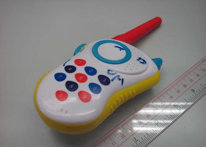
R55KS3159
Jun 01, 2012Handheld Walkie Talkies
Equipment Class
DXT - Part 15 Low Power Transceiver, Rx Verified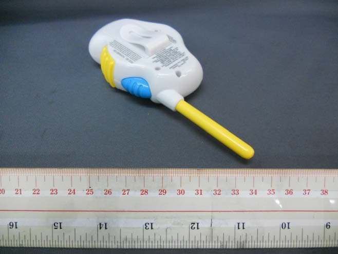
R55KSE120A
Jul 13, 2011Sesame Street Walkie Talkies
Equipment Class
DXX - Part 15 Low Power Communication Device Transmitter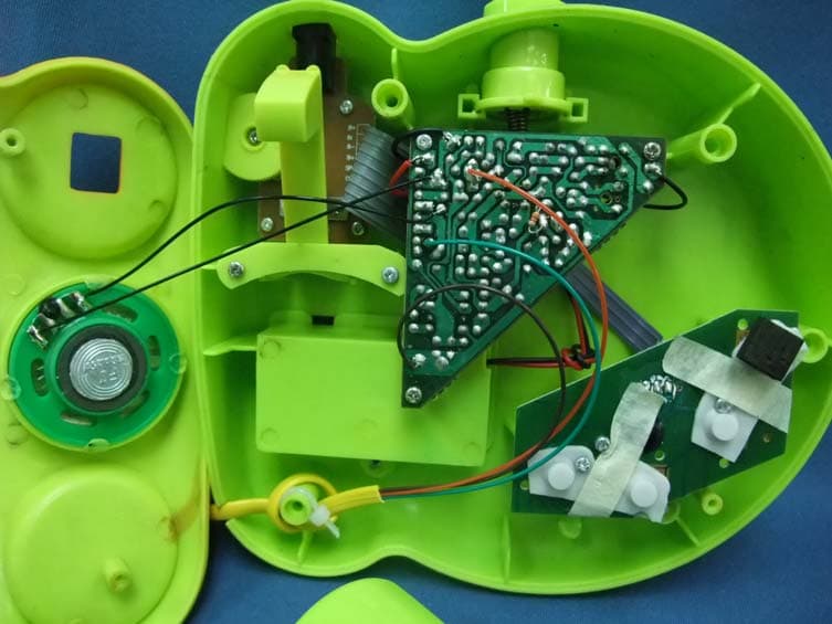
R55KS723
Aug 20, 2009Full duplex walkie talkie phone
Equipment Class
DXX - Part 15 Low Power Communication Device Transmitter
R55KSS9104
May 24, 20062-Way FRS Radio
Equipment Class
FRF - Part 95 Family Radio Face Held Transmitter