R73LPA-24G-12.4 GHz FHSS TRANSCEIVER
The Sapling Company, Inc
Click to zoom
Application Details
- Equipment Class
- DSS - Part 15 Spread Spectrum Transmitter
- Date of Grant
- Nov 17, 2013
- Application Purpose
- Original Equipment
- Date of Application
- Nov 17, 2013
- Equipment Note
- 2.4 GHz FHSS TRANSCEIVER
- Frequency Range
- 2433.00000000 - 2449.00000000
- Company
- The Sapling Company, Inc
- Country
- United States
Documents & Files
Document Text
Text extracted from the exhibit documents filed with the FCC. Open a document above to read the original.
Users Manual
USER MANUAL NOVEMBER 2013 2.433-2.449 GHz Frequency Hopping Transceiver Module Model: A-CCA-LPA-24G-1 FCC ID: R73LPA-24G-1 REV 4 Page 2 of 7 Introduction This module is only authorized to be installed in fixed mount installation and may not be installed in a mobile or portable device. The LPA-24G-1 RF module is to be used in Sapling Analog Clocks such as the SAL Series Clocks and equivalent models. The module is only to be connected to and installed in other Sapling products. Specifications The PCB antenna gain is +3.3dB maximum. The maximum output power will be 18 dBm. The transmit cycle is a sequence of 80 data strings on 76 different frequencies, each transmitted for 3 msec. Every transmit cycle is 240 msec in duration (80 x 3msec). The frequency hopping pattern is proprietary to Sapling and covers the range from 2.433 to 2.449 GHz. Connections The picture shows the LPA-24G-1 RF module, connectors, and FCC ID label. LPA-24G-1 FCC ID: R73LPA-24G-1 J4 POWER & DATA J3 PROGRAMMING Page 3 of 7 LPA-24G-1 Connectors J3 PROGRAMMING CONNECTOR PIN 1* TDO/TDI PIN 2 3.3 VOLTS PIN 3 TDI PIN 4 3.3 VOLTS PIN 5 S2 DRV (TMS) PIN 6 1.8 VOLTS PIN 7 TCLK PIN 8 TEST PIN 9 GROUND PIN 10 GROUND PIN 11 RST PIN 12 TXD PIN 13 SHIELD PIN 14 RXD * PIN 1 IS THE SQUARE PAD. J4 GEARBOX CONNECTOR PIN 1* MOT SEC 1 1.8 VOLTS PIN 2 MOT SEC 2 PIN 3 MOT MIN 1 1.8 VOLTS PIN 4 MOT MIN 2 PIN 5 GRBX SEL A PIN 6 GRBX SEL B PIN 7 PWR DET PIN 8 S1 PIN 9 GROUND PIN 10 S2 PIN 11 3.3 VOLTS PIN 12 GRBX DET PIN 13 1.8 VOLTS PIN 14 GROUND * PIN 1 IS THE SQUARE PAD. J3 PROGRAMMING J4 POWER & DATA Page 4 of 7 Installed The picture below shows the LPA-24G-1 RF module in an analog clock. It shows the SAL-GBS-09S-0, a battery powered wireless analog clock. SAL-GBS-09S-0 LPA-24G-1 J3 PROGRAMMING J4 POWER & DATA Page 5 of 7 The picture below shows the LPA-24G-1 RF module installed. The picture is the back of an SAL-GBS-09S-0, a battery powered wireless analog clock, and the FCC ID and the Compliance Label. SAL-GBS-09S-0 LPA-24G-1 INSTALLED INSIDE . J3 PROGRAMMING Page 6 of 7 SAL-GBS-09S-0 Label The label below is an example of the FCC ID and the Compliance Label. Operation 1. The line powered version of the LPA-24G-1 RF module will transmit the time for 240 msec and receive the time for up to 20 seconds once a minute. 2. The battery powered version of the LPA-24G-1 RF module will transmit the time for 240 msec and receive the time for up to 20 seconds every 2 hours. FCC Statement: This device complies with part 15 of the FCC Rules. Operation is subject to the following two conditions: (1) This device may not cause harmful interference, and (2) this device must accept any interference received, including interference that may cause undesired operation. NOTE: THE MANUFACTURER IS NOT RESPONSIBLE FOR ANY RADIO OR TV INTERFERENCE CAUSED BY UNAUTHORIZED MODIFICATIONS TO THIS EQUIPMENT. SUCH MODIFICATIONS COULD VOID THE USER’S AUTHORITY TO OPERATE THE EQUIPMENT. Changes Or Modifications Not Expressly Approved By The Party Responsible For Compliance Could Void The User's Authority To Operate The Equipment. Page 7 of 7 Antenna(s) This transmitter must be installed to provide a separation distance of at least 8.1 cm from all persons and must not be co-located or operating in conjunction with any other antenna or transmitter for satisfying RF exposure compliance.
Block Diagram
55 44 33 22 11 D D C C B B A A TitleSize Document Number Rev Date: Sheet of <Doc> 2.0 <Title> A 11 Monday, May 20, 2013 TitleSize Document Number Rev Date: Sheet of <Doc> 2.0 <Title> A 11 Monday, May 20, 2013 TitleSize Document Number Rev Date: Sheet of <Doc> 2.0 <Title> A 11 Monday, May 20, 2013 MOSIMISOCLKENABLE MSP430TEXAS INSTRUMENTS PROCESSOR CC2500TEXAS INSTRUMENTS RF TRANSCEIVER IC MATCHINGNETWORK SPI SERIAL COMMUNICATIONS "INVERTED F" PCB ANTENNA 2.4GHz LPA / BLOCK DIAGRAM +18 DBm OUTPUT @ 50 OHM CC2591TEXAS INSTRUMENTS RF FRONT-END IC 0 DBm OUTPUT @ 50 OHM HARMONIC FILTER #2 HARMONIC FILTER #1 Y1 32.768KHZ Y1 32.768KHZ Y226.000 MHzY226.000 MHz 43 12 ANT1 2.4GHz FREQUENCY ANT1 2.4GHz FREQUENCY
Cover Letter(s)
The Sapling Company, Inc. 215.322.6063 P. 1633 Republic Road 215.322.8498 F. Huntingdon Valley, PA 19006 www.sapling-inc.com Date: September 17, 2013 To: Federal Communications Commission Authorization and Evaluation Division From: Lars Jorgensen Subject: Agent Authorization for certification of FCC ID: R73LPA-24G-1 The Sapling Co Inc herby appoints Richard Reitz of Retlif Testing Laboratories to act as our agent in the matter of FCC filings for the certification of FCC ID: R73LPA-24G-1 The Sapling Co Inc further attests that no party to the application is subject to denial of federal benefits pursuant to section 5301 of the Anti-Drug Abuse Act of 1988, 21 USA 853(a). Sincerely, Lars Jorgensen Lars JorgensenLars Jorgensen Lars Jorgensen Lars Jorgensen QA Supervisor
Cover Letter(s)
The Sapling Company, Inc. 215.322.6063 P. 1633 Republic Road 215.322.8498 F. Huntingdon Valley, PA 19006 www.sapling-inc.com Date: September 17, 2013 To: Federal Communications Commission Authorization and Evaluation Division From: Lars Jorgensen Subject: Confidentiality Request regarding application for certification of FCC ID: R73LPA-24G-1 Pursuant to Sections 0.457 and 0.459 of the Commission’s rules, we hereby request confidential treatment of information accompanying this application as out lined below: Permanent Confidentiality Exhibit Type File Name Schematics R73LPA-24G-1Schem.pdf The above materials contain trade secrets and proprietary information not customarily released to the public. The public disclosure of these materials may be harmful to the applicant and provide unjustified benefits to its competitors. The applicant understands that pursuant to Section 0.457 of the Rules, disclosure of this application and all accompanying documentation will not be made before the date of the Grant for this application. Sincerely, Lars Jorgensen Lars JorgensenLars Jorgensen Lars Jorgensen Lars Jorgensen QA Supervisor The Sapling Co Inc
External Photos
The Sapling Company FCC ID: R73LPA-24G-1 External Photographs External AC Power External Battery Power The Sapling Company FCC ID: R73LPA-24G-1 External Photographs Clock Front Clock Back
ID Label/Location Info
The Sapling Company, Inc. 1633 Republic Road Huntingdon Valley, PA 19006 (215) 322-6063 www.sapling-inc.com The Sapling Company, Inc. 1633 Republic Road Huntingdon Valley, PA 19006 (215) 322-6063 www.sapling-inc.com November 01, 2013November 01, 2013Date:Date: SW-LPA-V2.0.2SW-LPA-V2.0.2 SAL SeriesSAL Series Input Voltage: 3V (2 'D' Cell)Input Voltage: 3V (2 'D' Cell) Quantity 1Quantity 1 A-MVLPA-100-ASY-UTS0/131101/T000046A-MVLPA-100-ASY-UTS0/131101/T000047 Made in U.S.A.Made in U.S.A. ↑ ↑ Diagnostic Switches ↑ ↑ Diagnostic Switches Diagnostic LED Diagnostic LED Diagnostic LED Diagnostic LED FCC ID:R73LPA-24G-1 Model: A-CCA-LPA-24G-1 This device complies with Part 15 of the FCC Rules. Operation is subject to the following two conditions: (1) this device may not cause harmful interference, and (2) this device must accept any interference received, including interference that may cause undesired operation. FCC ID:R73LPA-24G-1 Model: A-CCA-LPA-24G-1 This device complies with Part 15 of the FCC Rules. Operation is subject to the following two conditions: (1) this device may not cause harmful interference, and (2) this device must accept any interference received, including interference that may cause undesired operation.
ID Label/Location Info
The Sapling Company FCC ID: R73LPA-24G-1 Label Location The Sapling Company FCC ID: R73LPA-24G-1 Label Location
Internal Photos
The Sapling Company FCC ID: R73LPA-24G-1 Internal Photographs TOP BOTTOM The Sapling Company FCC ID: R73LPA-24G-1 Internal Photographs Internal AC Power Internal Battery Power
Operational Description
LPA-24G-1 Operational Description August 9, 2013 The information contained in this document is Proprietary and Confidential information of The Sapling Company Inc. GENERAL DESCRIPTION: The Low Power Analog Board (LPA) uses RF communications for building wide clock synchronization. The LPA uses the 2.4 GHz ISM frequency band to provide communications clock to clock. The LPA board uses the Texas Instruments CC2500 RF transceiver, the Texas Instruments CC2591 RF Front End and the Texas Instruments MSP430F2252 microcontroller. Other features include an "Inverted F" printed circuit board (PCB) pattern antenna design. The board shall meet all FCC requirements for license free operation in the 2.4GHz ISM band. The receiver input sensitivity shall be better that 104 dBm while transmitter output shall be up to 18 dBm. 1.1 Overview The LPA integrates the analog clock driver gearbox with an RF communications interface using the CC2500 RF transceiver chip as the basis for a complete RF transceiver. The microcontroller handles all time keeping functionality; it controls the hand movement of the gearbox and also controls the RF transceiver. It’s normally in sleep mode until an update is required, keeping the average power consumption very low in order to extend battery life. 1.2 RF Section The CC2500 is the heart of the RF section. It contains the input Low Noise Amplifier (LNA), mixer, synthesizer, demodulator, IF amplifier, RSSI circuitry, and transmit Power Amplifier (PA) in one chip. The CC2591 provides an additional LNA and transmit PA to boost the output further. The "Inverted F" PCB pattern antenna is used for both the transmit and receive paths. Provisions will be made for an optional SMA connector so that an external antenna can be attached for in-house testing only. This connector is not added to the circuit board in production. 1.2.1 Receive The input sensitivity of the CC2500 is typically -104 dBm. The printed circuit antenna will be filtered and matched to the CC2500 input. The CC2591 provides additional signal gain by use of its LNA. RF Network The transceiver is only on for few seconds every 2 hours for the battery clocks, or once a minute for line-powered clocks. The receiver turns ON 5 seconds before the estimated receive time and waits for up to 15 seconds to get the signal. During this time the receiver changes frequency every 3 ms. 1.2.2 Transmit The output of the CC2500 is connected to the PCB antenna through matching and filtering circuitry. The maximum output power of the Cc2500 is 0 dBm. This signal is amplified by the CC2591 and has a maximum output, after filtering, of 18 dBm presented to the antenna. The transmit cycle is a sequence of 80 data strings on 76 different frequencies, each transmitted for 3 msec. Every transmit cycle is 240 msec in duration (80 x 3ms). The frequency hopping pattern is proprietary to Sapling but covers the range from 2.433 Ghz to 2.449 Ghz. 1. Operational Description: There are 76 discrete channels used. The transmitter’s pseudorandom hoping sequence table is attached at the bottom of this document. There is a 200Khz separation between adjacent channels but because of the hopping, the closest carrier frequencies are 400 KHz apart. At each transmission cycle (once every minute), 80 channels are transmitted. Assume the transmitter begins at line #1 in the table (channel 43). Channels associated with lines 1 through 76 are transmitted, followed by transmitting channels associated with lines 1 through 4, for a total of 80 channels. After one minute, channels associated with lines 5-76 are transmitted, followed by transmitting channels associated with lines 1-8, for a total of 80 channels. After another minute, channels associated with lines 9-76 are transmitted, followed by transmitting channels associated with lines 1-12, again for a total of 80 channels. And so on. For example, after stopping at line 8 (channel 7), the next sequence starts at line 9 (channel 27). To be clear, Sapling’s clocks do not require receiving the time signal consistently because only a time correction is required. Each clock has an internal Real-Time-Clock that is reasonably accurate. Hence, the receivers are not synched to the transmitter in the normal use of frequency hopping systems. Any successfully received channel updates the internal Real-Time-Clock for the exact time. The system is much more random in terms of when the signal is received than standard hopping systems because so little data is exchanged (Time) and only one channel needs be successful in matching the receiver to the transmitter. The receiver and transmitter have the same bandwidth. The receiver is open for a maximum of 7 seconds, or until the data is received. The Receiver hops every 100ms. 2. External photos: Please provide clearer external photos, show the power and data or other connections. (Show All Sides) 3. Block diagram: Please show electrical and data connection to host devices. Sapling Proprietary Psedo-Random Hopping Table 2.4GHz Channel Frequencies and Sequencing Line # Start Frequency Step Next Channel Channel Frequency 1 2433 0.2 43 2441.6 2 2433 0.2 16 2436.2 3 2433 0.2 46 2442.2 4 2433 0.2 33 2439.6 5 2433 0.2 30 2439.0 6 2433 0.2 13 2435.6 7 2433 0.2 25 2438.0 8 2433 0.2 7 2434.4 9 2433 0.2 27 2438.4 10 2433 0.2 5 2434.0 11 2433 0.2 17 2436.4 12 2433 0.2 10 2435.0 13 2433 0.2 24 2437.8 14 2433 0.2 31 2439.2 15 2433 0.2 37 2440.4 16 2433 0.2 6 2434.2 17 2433 0.2 47 2442.4 18 2433 0.2 29 2438.8 19 2433 0.2 2 2433.4 20 2433 0.2 15 2436.0 21 2433 0.2 12 2435.4 22 2433 0.2 32 2439.4 23 2433 0.2 51 2443.2 24 2433 0.2 9 2434.8 25 2433 0.2 26 2438.2 26 2433 0.2 22 2437.4 27 2433 0.2 49 2442.8 28 2433 0.2 39 2440.8 29 2433 0.2 42 2441.4 30 2433 0.2 44 2441.8 31 2433 0.2 1 2433.2 32 2433 0.2 69 2446.8 33 2433 0.2 21 2437.2 34 2433 0.2 57 2444.4 35 2433 0.2 75 2448.0 36 2433 0.2 35 2440.0 37 2433 0.2 3 2433.6 38 2433 0.2 41 2441.2 39 2433 0.2 50 2443.0 40 2433 0.2 36 2440.2 41 2433 0.2 45 2442.0 …
Text truncated - open the document above for the full version.
Parts List/Tune Up Info
A-CCA-LPA-24G-1 REV 2c 5/23/2013 A-PCB-LPA-24G-1PCB For LPA Module 2.4GHz BD F 1.00Item: 1 LINECOMPONENTDESCRIPTION U/MLOCATION PART NUMBERMANUFACTURER 1 E-CR26MHZ-16PFCRYSTAL, 4-PIN, 26 MHZ, 16PF, 1.00Y2 ABMM2-26.000HMZ-16-1-B1-TAbracon Corporation 2 E-ICSN74LVC1G17Single Schmitt-Trigger Buffer 2.00U1,U2 SN74LVC1G17DBVRTexas Instruments 3 E-DO-NOT-POPDo Not Populate Component 20.00 C11,C31,C32,C33,C34,C43,C45,C51,C52,FL2,J1,J2,R3,R5,R7,RXXXXXXXXXX 4 E-DSBAT46JFILMDIODE SCHOTTKY SS SOD-323 1.00D1 BAT46JFILMSTMicroelectronics 5 E-DFBAV99LT1DIODE, SOT23, BAV99-TP, DUAL S 1.00D2 BAV99LT1GON Semiconductor 6 E-LEDAM2520CGCKLED, GREEN, SMT 2.5X2 1.00LED1 AM2520CGCK09Kingbright Corp 7 E-LEDAM2520ECLED, RED, SMT 2.5X2 1.00LED2 AM2520EC09Kingbright Corp 8 E-QMMBT4401WT1Transistor,Switching, NPN, SC- 4.00Q6,Q8,Q10,Q12 MMBT4401WT1GON Semiconductor 9 E-QMMBT4403WT1Transistor,Switching, PNP, SC- 6.00Q1,Q2,Q5,Q7,Q9,Q11 MMBT4403WT1GON Semiconductor 10E-SWTCH-TM116CLT SWITCH RT ANGLE L8.35MM, Ca 2.00SW1,SW2 EVQ-PF108KPanasonic - ECG 11E-CR32.7-ABS25Crystal, 32.768KHZ, 4-PIN, 6pf 1.00Y1 ABS25-32.768KHZ-6-1-TAbracon Corporation 12E-ICMSP430F2252IC,TSOP38,MSP430F2252,MICROCON 1.00U3 MSP430F2252IDARTexas Instruments 13E-ICNC7SZ14MIC, SOT23-5, NC7SZ14M5 or NC7S 2.00U6,U7 NC7SZ14M5XFairchild Semiconductor 14E-Q2222LT1SOT23Transistor NPN SOT23, 2N2222A 2.00Q3,Q4 MMBT2222AFairchild Semiconductor 15E-CC.1UF16V0402CAP CER 0.1UF 16V 20% 0402 Y5V 7.00C1,C2,C3,C4,C20,C44,C46 C0402C104M4VACTUKemet 16E-CCHF27PF50V42CER CAP, High-Freq 27 PF 50V+/ 11.00C7,C9,C10,C12,C13,C21,C25,C35,C36,C40,C42 500R07S270JV4TJOHANSON TECHNOLOGY INC (VA) 17E-CCHF220PF50V4CER CAP, High-Freq 220 PF 50V+ 3.00C14,C15,C38 GRM155R71H221KA01DMurata Electronics North America 18E-CCHF9.1PF50V4CER CAP, High-Freq, 9.1 PF 50V 2.00C23,C27 GJM1555C1H9R1CB01DMurata Electronics North America 19E-CCHF6.8PF50V4CER CAP, High-Freq 6.8 PF 50V+ 1.00C24 CBR04C689D5GACMurata Electronics North America 20E-CCHF.1UF10V42CER CAP, High-Freq 0.1 UF 10V 4.00C22,C26,C37,C39 C0402C104K8RACTUKemet 21E-CCHF1.5PF50V4CER CAP, High-Freq, 1.5 PF 50V 1.00C29 GJM1555C1H1R5CB01DMurata Electronics North America 22E-CCHF1PF50V402 CER CAP, Hi-Freq 1.0 PF 50V+/-.1PF 0402 2.00 C17,C53GJM1555C1H1R0BB01DMurata 23E-CCHF2.2UF6.3VCER CAP, High-Freq 2.2 UF 6.3V 2.00C47,C49 GRM155R60J225ME15DMurata 24E-CCHF100PF50V4CER CAP, High-Freq 100 PF 50V+ 3.00C30,C48,C50 GRM1555C1H101JZ01DMurata Electronics North America 25E-CONFR2X7TH0.1CON,RF,2X7,0.1 1.00J3 SSW-107-02-G-D-RASamtec Inc 26E-CONF2X7TH0.1CON,F,2X7,0.1SP, HT.335 Female Conn 1.00J4 SSW-107-01-F-DSamtec Inc 27E-INLQW15AN4N3CINDUCTOR,0402, 4.3NH,750mA,+/- 2.00L1,L3 LQW15AN4N3C00DMurata Electronics North America 28E-INLQW15AN1N5BINDUCTOR,0402, 1.5NH,1000mA,+/ 1.00L2 LQW15AN1N5B00DMurata Electronics North America 29E-CCHF0.7PF50V4 CER CAP,Hi-Freq, 0.7 PF 50V+/-0.05pF 040 1.00 C28 GJM1555C1HR70WB1DMurata 30E-INBLM15HB221SChip Ferrite Bead, 220 OHM 250 2.00L5,L6 BLM15HB221SN1DMurata Electronics North America 31E-R47K5%0402RES 47K OHM 5% 1/16W 0402 SMD 1.00R1 RC0402JR-0747KLYageo 32E-CC2.2PF50V402CER CAP 2.2PF 50V+/-.25PF 0402 2.00C5,C6GRM1555C1H2R2CZ01DMurata 33E-R0-5%0402RES 0 OHM 5% 1/16W 0402 SMD 10.00 R2,R4,R6,R8,R15,R16,R30,R47,R48,R49 RC0402JR-070RLYageo 34E-R220-5%0402RES 220 OHM 5% 1/16W 0402 SMD 1.00 R11 RC0402JR-07220RLYageo 35E-R10K5%0402RES 10K OHM 5% 1/16W 0402 SMD 11.00 R12,R13,R31,R32,R33,R34,R38,R39,R40,R41,R42 RC0402JR-0710KLYageo 36E-R100K5%0402RES 100K OHM 5% 1/16W 0402 SMD 2.00R14,R45 RC0402FR-07100KLYageo 37E-R100-5%0402RES 100 OHM 5% 1/10W 0402 SMD 9.00R17,R18,R23,R24,R25,R28,R35,R36,R37 RC0402JR-07100RLYageo 38E-R470-5%0402RES 470 OHM 5% 1/10W 0402 SMD 2.00R19,R20 RC0402JR-07470RLYageo 39E-R56K1%0402RES 56K OHM 1% 1/10W 0402 SMD 1.00R26 RC0402FR-0756KLYageo 40E-R51K5%0402RES 51K OHM 1/10W 5% 0402 SMD 1.00R46 RC0402FR-0751KLYageo 41E-CON1X1TH0.1Connector, TSW-101-07-G-S Samt 2.00TP4,TP5 TSW-101-07-G-SSamtec Inc 42E-ICCC2500RTKRIC RF TXRX SNGL-CHIP LP 20-QFN 1.00U4 CC2500RTKRTexas Instruments 43E-ICCC2591RGVIC RF FRONT END 2.4GHZ 16QFN 1.00U5 CC2591RGVRTexas Instruments 44E-R4.3K1%0402RES 4.3K OHM 1/10W 1% 0402 SMD 3.00R27,R9,R10 RC0402FR-074K3LYageo 45E-CCHF15PF50V42CER CAP, High-Freq 15 PF 50V+/ 1.00C41 GJM1555C1H150JB01DMurata 46E-CCHF1000PF50VCER CAP, High-Freq,1000 PF 50V 4.00C8,C16,C18,C19 GRM1555C1H102JA01DMurata 47E-INLQG15SH1N1SINDUCTOR,0402, 1.1NH,300mA,+/- 1.00L7 LQG15HS1N1S02DMurata 48E-INLQG15HS5N1SINDUCTOR,0402, 5.1NH,300mA,+/- 1.00L8 LQG15HS5N1S02DMurata 49E-FL748112024RF Filter, Low Pass WE-LPF 1.00 FL1 748112024WURTH ELECTRONICS 50E-INLQG15HS3N3SINDUCTOR,0402, 3.3NH,300mA,+/-0.3 1.00L4 LQG15HS3N3S02DMurata 51E-INLQG15HS2N7SINDUCTOR,0402, 2.7NH,300mA,+/-0.31.00 L9 LQG15HS2N7S02DMurata Circuit Card Assy, LPA 2.4GHz for Wireless Analog Clocks The Sapling Company, Inc. (SAP)
Test Report
Report No. R-1861P-2, Rev A. Page 2 of 32 Retlif Testing Laboratories R Technical Information Report Number: R-1861P-2, Rev. A Customer: The Sapling Company, Inc. Address: 1633 Republic Road Huntingdon, PA 19006 Manufacturer: The Sapling Company, Inc. Manufacturer Address: 1633 Republic Road Huntingdon, PA 19006 Test Sample: FHSS Transceiver Model Number: A-CCA-LPA-24G-1 FCC ID: R73LPA-24G-1 Type: 2.433 to 2.449 GHz Frequency Hopping Spread Spectrum Transceiver Power Requirements: 3 VDC Derived from (2) ‘D’ Cell Batteries or 120 VAC, 60 Hz Frequency of Operation: 2.433 to 2.449 GHz Equipment Class: DSS Equipment Use: Fixed Test Specification: FCC Rules and Regulations Part 15, Subpart C, Section 15.247 Test Procedure: ANSI C63.4:2003 Filing and Measurement Guidelines for Frequency Hopping Spread Spectrum Systems, FCC: DA 00-705 Test Facility: Retlif Testing Laboratories 3131 Detwiler Road Harleysville, PA 19438 FCC Registered Test Site Number: 98314 Report No. R-1861P-2, Rev A. Page 3 of 32 Retlif Testing Laboratories R Tests Performed The test methods performed on the FHSS Transceiver Module are shown below. Table 1 - Test Methods Performed FCC Part 15, Subpart C Test Method 15.247(a)(1) Channel Separation 15.247(a)(1) 20 dB Bandwidth 15.247(a)(1)(iii) Number of Channels and Occupancy Time 15.247(b)(1) and (4) Peak Conducted Output Power - Alternate Procedure 15.247(d) Spurious Radiated Emissions, 30 kHz to 25 GHz 15.247(d) Spurious RF Conducted, 30 MHz to 25 GHz - Alternate Procedure 15.207(a) Conducted Emissions, Power Leads, 150 kHz to 30 MHz Report No. R-1861P-2, Rev A. Page 5 of 32 Retlif Testing Laboratories R Requirements and Test Results Requirement: FCC Section 15.247 (a)(1) Channel Separation and 20 dB Bandwidth Frequency hopping systems shall have hopping channel carrier frequencies separated by a minimum of 25 kHz or the 20 dB bandwidth of the hopping channel, whichever is greater. Alternatively, frequency hopping systems operating in the 2400-2483.5 MHz band may have hopping channel carrier frequencies that are separated by 25 kHz or two-thirds of the 20 dB bandwidth of the hopping channel, whichever is greater, provided the systems operate with an output power no greater than 125 mW. The system shall hop to channel frequencies that are selected at the system hopping rate from a pseudo randomly ordered list of hopping frequencies. Each frequency must be used equally on the average by each transmitter. The system receivers shall have input bandwidths that match the hopping channel bandwidths of their corresponding transmitters and shall shift frequencies in synchronization with the transmitted signals. Results: The carrier frequencies were separated by 200 kHz which complied with the requirements specified above. FCC Section 15.247 (a)(1)(iii) Number of Channels and Occupancy Time Frequency hopping systems operating in the 2400-2483.5 MHz band shall use at least 15 channels. The average time of occupancy on any channel shall not be greater than 0.4 seconds within a period of 0.4 seconds multiplied by the number of hopping channels employed. Frequency hopping systems may avoid or suppress transmissions on a particular hopping frequency provided that a minimum of 15 channels are used. The test sample utilized 76 channels. The average Time of Occupancy was not greater than 0.4 seconds with a period of 30 seconds. Report No. R-1861P-2, Rev A. Page 6 of 32 Retlif Testing Laboratories R Requirements and Test Results (con’t) FCC Section 15.247 (b)(1) and (4) Peak Conducted Output Power (1) For frequency hopping systems operating in the 2400-2483.5 MHz band employing at least 75 non-overlapping hopping channels, and all frequency hopping systems in the 5725-5850 MHz band: 1 watt. For all other frequency hopping systems in the 2400-2483.5 MHz band: 0.125 watts. (4) The conducted output power limit specified in Paragraph (b) of Section 15.247 is based on the use of antenna with directional gains that do not exceed 6 dBi. Except as shown in Paragraph (c) of Section 15.247, if transmitting antennas of directional gain greater than 6 dBi are used, the conducted output power from the intentional radiator shall be reduced below the stated values in Paragraph (b)(1), (b)(2) and (b)(3) of Section 15.247, as appropriate, by the amount in dB that the directional gain of the antenna exceeds 6 dBi. Results The frequency hopping system utilized a transmitting antenna with a directional gain of 3.3 dBi therefore, the peak output power limit was 1 watt. The maximum peak conducted output power was measured to be 382.0 milliwatts. FCC Section 15.247(d) Spurious Emissions In any 100 kHz bandwidth outside the frequency band in which the spread spectrum or digitally modulated intentional radiator is operating, the radio frequency power that is produced by the intentional radiator shall be at least 20 dB below that in the 100 kHz bandwidth within the band that contains the highest level of the desired power, based on either an RF conducted or a radiated measurement, provided the transmitter demonstrates compliance with the peak conducted power limits. If the transmitter complies with the conducted power limits based on the use of RMS averaging over a time interval, as permitted under Paragraph (b)(3) of Section 15.247, the attenuation required under this paragraph shall be 30 dB instead of 20 dB. Attenuation below the general limits specified in Section 15.209(a) is not required. In addition, radiated emissions which fall in the restricted bands, as defined in Section 15.205(a) must also comply with the radiated emission limits specified in Section 15.209(a) (see Section 15.205(c)). Results The antenna conducted spurious emissions comply with the requirement that the radio frequency power be at least 20 dB below the highest in band level. In addition, Harmonic and Spurious Emissions which were found to be within the restricted bands of operation, as defined in section 15.205(a) were found to be i…
Text truncated - open the document above for the full version.
Test Report
Design Note DN0007 2.4 GHz Inverted F Antenna By Audun Andersen Keywords • CC2400 • CC2420 • CC2430 • CC2431 • CC2500 • CC2510 • CC2511 • CC2550 • CC2520 • CC2480 • PCB Antenna • 2.4 GHz • Inverted F Antenna 1 Introduction This document describes a PCB antenna design that can be used with all 2.4 GHz transceivers and transmitters from Texas Instruments. Maximum gain is measured to be +3.3 dB and overall size requirements for this antenna are 25.7 x 7.5 mm. Thus, this is a compact, low cost and high performance antenna. SWRU120B Page 1 of 14 Design Note DN0007 Table of Contents KEYWORDS..............................................................................................................................1 1 INTRODUCTION.............................................................................................................1 2 ABBREVIATIONS...........................................................................................................2 3 DESCRIPTION OF THE INVERTED F ANTENNA DESIGN.........................................3 3.1 IMPLEMENTATION OF THE INVERTED F ANTENNA..........................................................3 4 RESULTS........................................................................................................................4 4.1 RADIATION PATTERN..................................................................................................4 4.2 REFLECTION............................................................................................................11 4.3 BANDWIDTH.............................................................................................................11 5 CONCLUSION ..............................................................................................................12 6 REFERENCES ..............................................................................................................13 7 GENERAL INFORMATION..........................................................................................14 7.1 DOCUMENT HISTORY................................................................................................14 2 Abbreviations CC2480 Z-Accel ZigBee Processor EM Evaluation Module IFA Inverted F Antenna ISM Industrial, Scientific, Medical PCB Printed Circuit Board SWRU120B Page 2 of 14 Design Note DN0007 3 Description of the Inverted F Antenna Design Since the impedance of the Inverted F Antenna is matched directly to 50 ohm no external matching components are needed. 3.1 Implementation of the Inverted F Antenna It is important to make an exact copy of the antenna dimensions to obtain optimum performance. The easiest approach to implement the antenna in a PCB CAD tool is to import the antenna layout from either a gerber or DXF file. Such files are included in CC2430DB reference design [1]. The gerber file is called “Inverted_F_Antenna.spl” and the DXF file is called “Inverted_F_Antenna.dxf”. If the antenna is implemented on a PCB that is wider than the antenna it is important to avoid placing components or having a ground plane close to the end points of the antenna. If the CAD tool being used doesn’t support import of gerber or DXF files, Figure 1 and Table 1 can be used. Figure 1. IFA Dimensions H1 5.70 mmW2 0.46 mm H2 0.74 mmL1 25.58 mm H3 1.29 mmL2 16.40 mm H4 2.21 mmL3 2.18 mm H5 0.66 mmL4 4.80 mm H6 1.21 mmL5 1.00 mm H7 0.80 mmL6 1.00 mm H8 1.80 mmL7 3.20 mm H9 0.61 mmL8 0.45 mm W1 1.21 mm Table 1. IFA Dimensions Since there is no ground plane beneath the antenna, PCB thickness will have little effect on the performance. The results presented in this design note are based on an antenna implemented on a PCB with 1 mm thickness. SWRU120B Page 3 of 14 Design Note DN0007 4 Results All results presented in this chapter are based on measurements performed with CC2430DB [1]. 4.1 Radiation Pattern Figure 2 shows how to relate all the radiation patterns to the orientation of the antenna. The radiation patterns were measured with CC2430 programmed to 0 dBm output power. XY plane XZ plane YZ plane Figure 2. How to Relate the Antenna to the Radiation Patterns SWRU120B Page 4 of 14 Design Note DN0007 Figure 3. XY Plane Vertical Polarization SWRU120B Page 5 of 14 Design Note DN0007 Figure 4. XY Plane Horizontal Polarization SWRU120B Page 6 of 14 Design Note DN0007 Figure 5. XZ Plane Vertical Polarization SWRU120B Page 7 of 14 Design Note DN0007 Figure 6. XZ Plane Horizontal Polarization SWRU120B Page 8 of 14 Design Note DN0007 Figure 7. YZ Plane Vertical Polarization SWRU120B Page 9 of 14 Design Note DN0007 Figure 8. YZ Plane Horizontal Polarization SWRU120B Page 10 of 14 Design Note DN0007 4.2 Reflection Figure 9. Measured Reflection at the Feed Point of the Antenna Figure 9 show that the IFA ensures less than 10 % reflection of the available power for a bandwidth of more than 300 MHz. A large bandwidth makes the antenna less sensitive to detuning due to plastic encapsulation or other objects in the vicinity of the antenna. 4.3 Bandwidth Another way of measuring the bandwidth after the antenna is implemented on a PCB and connected to a transmitter is to write test software that steps a carrier across the frequency band of interest. By using the “Max hold” function on a spectrum analyzer the variation in output power across frequency can easily be measured. Figure 10 shows how the output power varies on the IFA when the PCB is horizontally oriented and the re…
Text truncated - open the document above for the full version.
Contact Information
Applicant
Evgeny Raskin
Test Firm
Retlif Testing LaboratoriesMichael Bozza
Technical Specifications
| # | Rule Parts | Frequency Range | Power Output |
|---|---|---|---|
| 1 | 15C | 2.43 GHz - 2.45 GHz | 382.00 mW |
Other Applications from The Sapling Company, Inc

R73HPB-24G-1
Aug 25, 20132.4GHz FHSS TRANSCEIVER
Equipment Class
DSS - Part 15 Spread Spectrum Transmitter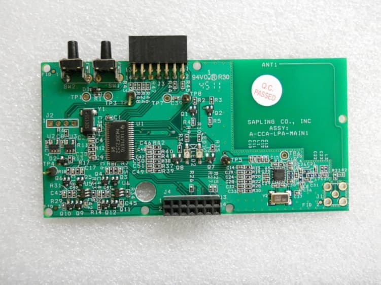
R73LPA1
Jun 19, 2012914 TO 928 MHz FREQUENCY HOPPING TRANSCEIVER MODULE
Equipment Class
DSS - Part 15 Spread Spectrum Transmitter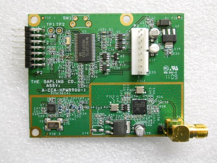
R73HPB1
May 20, 2012914 TO 928 MHz FREQUENCY HOPPING TRANSCEIVER MODULE
Equipment Class
DSS - Part 15 Spread Spectrum Transmitter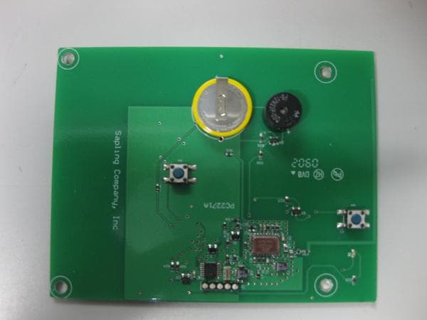
R73ERS003
Jul 04, 2010EMERGENCY RESPONSE SYSTEM (ERS) BATH STATION
Equipment Class
DXX - Part 15 Low Power Communication Device Transmitter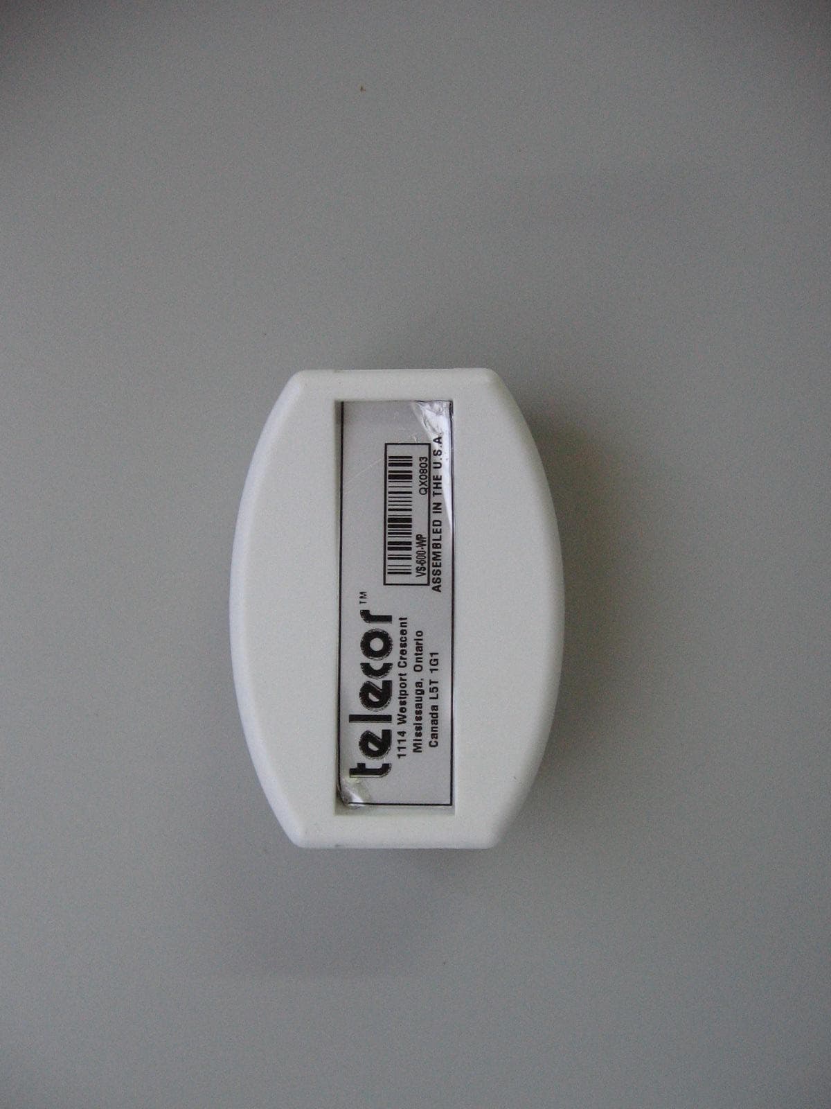
R73ERS002
Apr 28, 2010EMERGENCY RESPONSE SYSTEM (ERS) WIRELESS PENDANT
Equipment Class
DSR - Part 15 Remote Control/Security Device Transceiver