RAYGPS4000GPS Bluetooth Receiver
Navico Inc.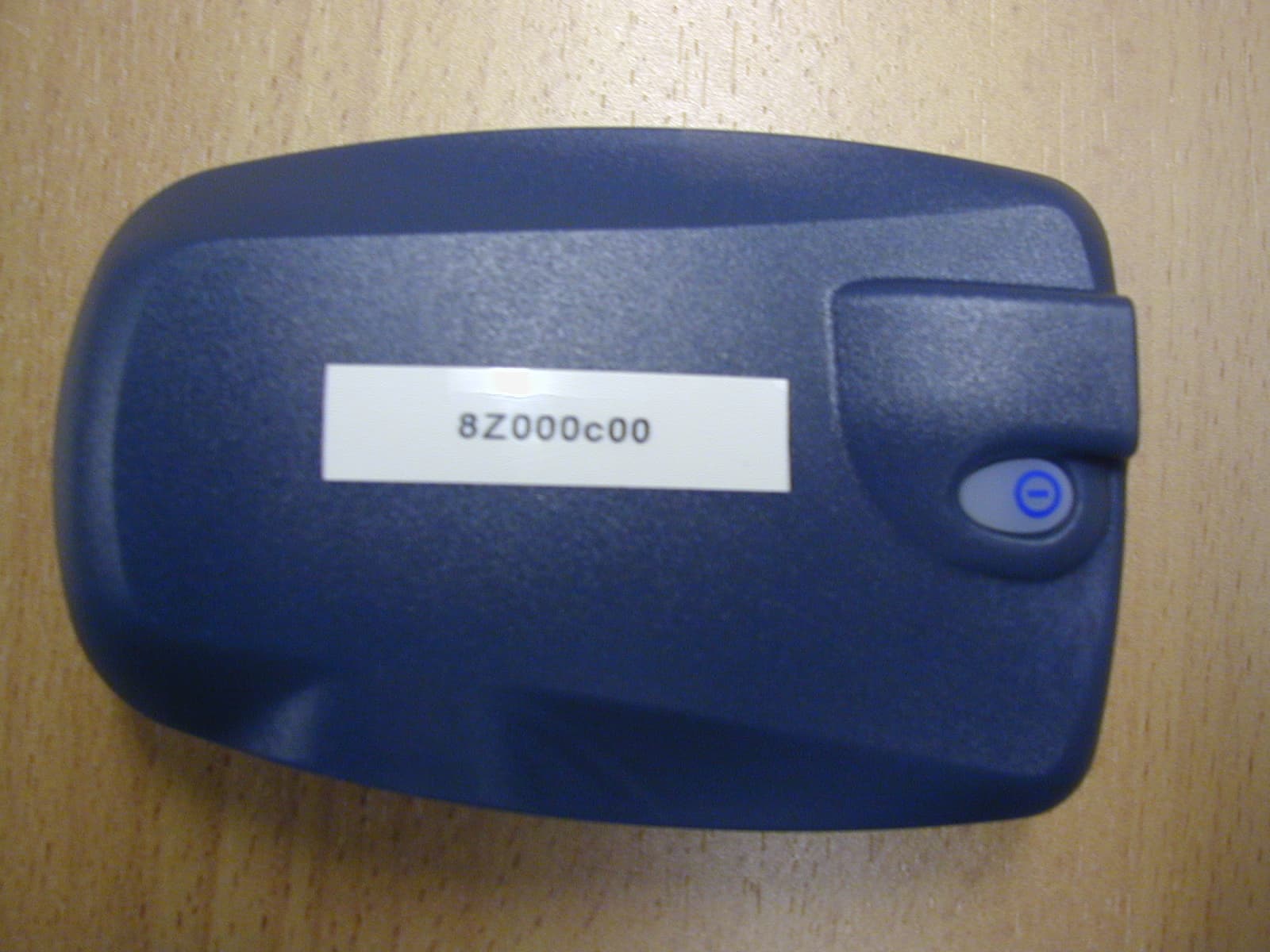
Click to zoom
Application Details
- Equipment Class
- DSS - Part 15 Spread Spectrum Transmitter
- Date of Grant
- Aug 19, 2003
- Application Purpose
- Original Equipment
- Date of Application
- Aug 19, 2003
- Equipment Note
- GPS Bluetooth Receiver
- Frequency Range
- 2402.00000000 - 2480.00000000
- Company
- Navico Inc.
- Country
- United States
Documents & Files
Document Text
Text extracted from the exhibit documents filed with the FCC. Open a document above to read the original.
Users Manual
1 GPS Bluetooth Receiver Installation and Operation Manual NAVMAN Installation and Operation Manual www.navman.com GPS BLUETOOTH RECEIVER GPS 4400 and GPS 4500 NAVMAN 3 GPS Bluetooth Receiver Installation and Operation Manual NAVMAN It is the owner’s sole responsibility to install and use the GPS Bluetooth Receiver in a manner that will not cause accidents, personal injury or property damage; will not obstruct your view; and will not interfere with the operation of the vehicle or the vehicle safety equipment. Using the GPS Bluetooth Receiver: •The US government is solely responsible for the operation, accuracy and maintenance of the GPS satellites. The GPS system is subject to changes that will affect the performance and accuracy of all GPS receivers. •The GPS signals may very occasionally be turned off. This antenna unit will not work if its batteries are flat. You must guard against these events by always having another way of navigating. •The GPS Bluetooth Receiver complies with CE and FCC standards for radio frequency interference. However, the unit receives and generates radio frequency energy. For reliable operation it must be mounted correctly, as described in this manual. •The performance of the receiver can be affected by the failure of a part, environmental conditions and improper installation and use. NAVMAN NZ LIMITED DISCLAIMS ALL LIABILITY FOR ANY USE OF THIS PRODUCT IN A WAY THAT MAY CAUSE ACCIDENTS OR DAMAGE OR THAT MAY VIOLATE THE LAW. This manual represents the receiver as at the time of printing. Navman NZ Limited reserves the right to make changes to specifications without notice. Governing Language: This statement, any instruction manuals, user guides and other information relating to the product (Documentation) may be translated to, or has been translated from, another language (Translation). In the event of any conflict between any Translation of the Documentation, the English language version of the Documentation will be the official version of the Documentation. Copyright © 2003 Navman NZ Limited, New Zealand. All rights reserved. NAVMAN is a registered trademark of Navman NZ Limited. FCC Statement Note: This equipment has been tested and found to comply with the limits for a Class B digital device, pursuant to Part 15 of the FCC Rules. These limits are designed to provide reasonable protection against harmful interference in a normal installation. This equipment generates, uses and can radiate radio frequency energy and, if not installed and used in accordance with the instructions, may cause harmful interference to radio communications. However, there is no guarantee that interference will not occur in a particular installation. If this equipment does cause harmful interference to radio or television reception, which can be determined by turning the equipment off and on, the user is encouraged to try to correct the interference by one or more of the following measures: •Reorient or relocate the receiving antenna •Increase the separation between the equipment and receiver •Connect the equipment into an output on a circuit different from that to which the receiver is connected •Consult the dealer or an experienced technician for help •A shielded cable must be used when connecting a peripheral to the serial ports. Compliance is subject to approval Important 4 GPS Bluetooth Receiver Installation and Operation Manual NAVMAN 1 Introduction The US Government operates the GPS system. Twenty-four satellites orbiting the earth broadcast timing signals which are freely available to use. The positions of these satellites are constantly changing. The GPS receiver tracks signals from all satellites visible above the horizon and uses measurements from all satellites more than 10° above the horizon to calculate exactly where it is on earth. This is called the GPS position. A GPS receiver can receive signals from the GPS satellites when it is almost anywhere on earth. The receiver is accurate even at high speeds and accelerations. •Extremely long battery life; around 40 hours of operation from one set of AAA alkaline batteries. (2 second update, trickle power mode) •No operator setup or adjustment required; the only operator control is the On/Off switch. •25 x 25 x 4 mm (1 x 1 x 0.2 in) patch GPS antenna with sensitive 12-channel GPS receiver chipset. •Available in two versions. These are identical except for resistance to water: The GPS 4500 is fully waterproof and is designed to be mounted outdoors, for example on the roof of a vehicle. The GPS 4400 is not waterproof and is designed to be mounted indoors. •An MCX connector for an external GPS antenna and a connector for an external power supply (GPS 4400 only). Cleaning and maintenance Clean the receiver with a damp cloth or mild detergent. Avoid abrasive cleaners, petrol or other solvents. Do not paint the receiver. Bluetooth is an industry standard wireless network for linking peripherals to Bluetooth enabled portable computers or PDAs. Bluetooth is fast, economical The GPS Bluetooth Receiver is a peripheral for a portable computer or PDA which calculates where the receiver is on earth. The receiver has: •A GPS antenna and GPS chipset to receive GPS signals and calculate the GPS position of the receiver. •A Bluetooth link to send the GPS position to a portable computer or PDA. The receiver is powered by its own internal batteries. In a typical land navigation application (see below), the GPS Bluetooth Receiver is mounted on a vehicle and sends the GPS position to a portable computer or PDA in the vehicle for use by a navigation application. GPS antenna GPS Bluetooth Receiver Portable computer or PDA (Bluetooth enabled) Bluetooth link Batteries GPS chipset Radio signals from GPS satellites Bluetooth network radio signals Bluetooth link Navigation application and uses little power. The GPS Bluetooth Receiver uses a Class 2 Bluetooth link, with a range of at least 10 m (33 ft). Features of the GPS Bluetooth Receiver What is Bl…
Text truncated - open the document above for the full version.
Users Manual
85 NAVMAN GPS 4400_ver04 ý 19-2 FCC Statement Note: This equipment has been tested and found to comply with the limits for a Class B digital device, pursuant to Part 15 of the FCC Rules. These limits are designed to provide reasonable protection against harmful interference in a normal installation. This equipment generates, uses and can radiate radio frequency energy and, if not installed and used in accordance with the instructions, may cause harmful interference to radio communications. However, there is no guarantee that interference will not occur in a particular installation. If this equipment does cause harmful interference to radio or television reception, which can be determined by turning the equipment off and on, the user is encouraged to try to correct the interference by one or more of the following measures: Reorient or relocate the receiving antenna. Increase the separation between the equipment and receiver. Connect the equipment into an output on a circuit different from that to which the receiver is connected. Consult the dealer or an experienced technician for help. A shielded cable must be used when connecting a peripheral to the serial ports. CAUTION: Changes or modifications not expressly approved by the party responsible for compliance could void the user's authority to operate the equipment.
Users Manual
Bluespark Technical Overview 25/3/03 D.Swarbrick Bluespark is a battery operated GPS receiver that transmits the NMEA data to a remote host using the Bluetooth protocol. The schematic is divided in to four sections: Page 1. GPS RF front end and Receiver. Page 2. GPS processor and flash memory. Page 3. Bluetooth transceiver/processor and flash memory. Page 4. Power supplies and logic translation. GPS RF front end and Receiver. GPS signals on 1575.42 MHz are picked up by the dielectric patch antenna (P1) and amplified by the LNA, Q4, whose bias is controlled/switched by Q1. Q3-A and Q3-B form a high side comparator sensing the voltage across R38 when current is drawn by an external antenna applied to J2. Q2-A and Q2-B buffer the comparator output and switch pin diode D10 on while switching Q1 off, thus selecting the external antenna while shutting off the LNA and hence the internal antenna. Note that the external antenna is applied after the on board LNA and assumes an active gain in the order of 18-30dB. (3V source, 5-20mA operating current) Q14 provides the processor with a level translated, active low flag to indicate that an external antenna is applied. U6 is a low noise 2.8V regulator providing power to the RF section and is controlled via the RFPC0 line from the processor when using trickle mode. Q15 and Q6 are also controlled from this line and switch off power to the external antenna when in trickle mode in order to conserve battery power. Signals from the selected source (either int. or ext. antenna) are presented to FL2, a SAW filter on 1575.42MHz to remove out of band signals before being input to U4, the SiRF RF IC. The GPS TCXO, Y5, and resonant circuit C96, L7 provide a clean, stable oscillator source. The SiRF RF IC uses a superheterodyne principle with a VCO local oscillator on 1565.97MHz and an IF of 9.45MHz. 2 bit sign and magnitude data is sent to the SiRF processor while RF power and AGC control signals are received. GPS processor and flash memory. The GPS processor is based on the ARM7 CPU and runs a 1.8V core with 3.3V I/O. It is a true system on a chip and contains at least the following functions: 1Mbit SRAM, Boot ROM, Real Time Clock, GPS DSP, Battery backed SRAM, Beacon DSP, SPI bus, I/O unit and Dual UARTs. Refering to page 2 of the schematic, U10 is a voltage monitor providing an active low reset to the processor if the 3V SiRF Vcc drops below 2.8V. D6 provides a non-return charging path (when the GPS is active) for the 3V MS Li-Ion battery (BT1) which supplies the RTC and BBSRAM via U18, a 1.8V regulator, when main batteries/ext power is absent. When either the internal batteries or the external power source is available, an alternative path is provided via D1 and DC_IN. Q7-A provides a level translated active low flag to the processor when external power is available thus allowing mode switching and the benefits of full power GPS to be realised. SIRF_TX and SIRF_RX are the main UART outputs (non-inverted TTL, 57600,8N1) carrying the NMEA data. Bluetooth transceiver/processor and flash memory. U3 is the BlueCore 2 single chip Bluetooth system incorporating 2.4GHz transmit/receive and baseband functions. Data originating from the GPS is presented to BC_RX, the BC2 UART input, for processing and eventual transmission as RF. Timing for all processor and RF synthesis is provided by the 16MHz crystal Y1. When transmitting, the outgoing balanced RF is first matched and converted to 50 ohm single ended by inductors L2, L3 and balun Y2. Filter Y3 provides harmonic and spurious output rejection before signals are passed to the chip antenna. Note that DC is provided to the push-pull output section of the BC2 via the balun. In receive, the reverse order of operation applies – signals from the 50 ohm chip antenna are first filtered (out of of band signals) then translated to a balanced input, under control of the internal T/R switch. U5 is a 4Mbit 1.8V flash memory that directly interfaces with the BC2. Q13-A and Q13-B buffer and translate the PIO ports to provide LED indicators for low battery (DS1, Red) and Bluetooth status (DS2, Blue). Power supplies and logic translation. 3 x AAA cells provide the main (int) power and this supply goes via the reverse battery protection device, Q5, to the 3V switching regulator, U13. Low battery status is monitored by U9 which outputs an active low to both the SiRF and BC2 processors, via D5, when level drops below 3.2V. J3 is the external 5V DC input socket. D2 provides reverse polarity protection while U11, a precision shunt regulator, conducts if the supply goes over 5.7V, saturating Q16 and shutting off Q17. This open circuit over voltage protection serves to protect U13 but is not intended to duplicate the full automotive load dump already provided in the 12V to 5V cigarette adaptor. When the On/Off switch, S3, is pressed, Q9 turns on and provides an enable to U13, the 3V switchmode regulator. This provides power to U7, which outputs 1.8V to the BC2. The BC2 then outputs a logic high to PWR_ON, switching on Q8-A and effectively latching the power switch on. If the BC2 is already powered on then pushing the switch S3 again will turn on Q8-B, providing the BC2 with a logic high on PWR_OFF and initiating the power down sequence. Q18 and Q19 allow the BC2 to control the 3V GPS supply, saving power when the Bluetooth link is lost or yet to be acquired. Q10-A and Q10-B provide inversion (2 stages), buffering and level translation for the SIRF_TX to BC_RX data path, with a tap mid way to the flash/program adaptor plug, J1. Similarly, Q11-A and Q11-B provide the same for the BC_TX to SIRF_RX data path. Q12-A and Q12-B provide translation from the BC2 GPIO to allow the SiRF processor to be reflashed. A tap between these devices also goes to J1. J1 is a diagnostic/test connector accessing most of the control and monitoring points needed to flash either the GPS or Bluetooth functions (even simultaneously).
Cover Letter(s)
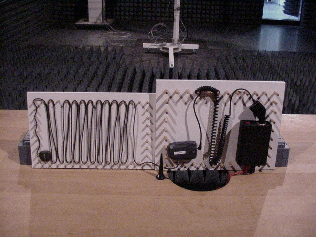
Exhibits for the TCB approval application ‘GPS Bluetooth Receiver’ Navman NZ Ltd. – FCC-ID: RAYGPS4000 Ex- hibit Description file name file type confi- dential A Agent authorization letter A_agent_authorization_letter pdf no B FCC test report B_4_7L_UK_0203_BTT_FCCa_FCC_15_247 pdf no C technical specification C_Technical Specification doc yes D FCC ID label and placement D_Navman GPS400 Series Label Rev1 doc no E Schematics E_schematics pdf yes F PCB layout 1 F_layout_LAYER1 pdf yes PCB layout 2 F_layout_LAYER2 pdf yes PCB layout 3 F_layout_LAYER3 pdf yes PCB layout 4 F_layout_LAYER4 pdf yes PCB layout 5 F_layout_LAYER5 pdf yes PCB layout 6 F_layout_LAYER6 pdf yes PCB layout 7 F_layout_NPTH_ROUTE pdf yes PCB layout 8 F_layout_PANEL_DRAWING pdf yes PCB layout 9 F_layout_PCB_STACK-UP pdf yes PCB layout 10 F_layout_PTH_ROUTE pdf yes PCB layout 11 F_layout_SOLDERMASK_BOT pdf yes PCB layout 12 F_layout_SOLDERMASK_TOP pdf yes PCB layout 13 F_layout_V-GROOVE pdf yes PCB layout 14 F_SILKSCREEN_BOT pdf yes PCB layout 15 F_SILKSCREEN_TOP pdf yes G Parts List G_bill_of_material xls yes H Request for confidentiality H_FCC Confidentiality Letter pdf no I Block diagram I_BlockDiagrams pdf yes Internal photo: housing J_photo_GPS4400battery-compartment jpg No J Internal photo: housing J_photo_GPS4400battery-compartment jpg No Internal photo: PCB bottom K_photo_GPS4400PCB-bottom jpg no K Internal photo: PCB top K_photo_GPS4400PCB-top jpg no L External photo top L_photo_GPS4400top jpg no M External photo bottom M_photo_GPS4400bottom jpg no Photos: test setup 1 N_testsetup1 jpg no N Photos: test setup 2 N_testsetup2 jpg no O users guide O_users_manual pdf no O_Functional_Description doc no P Additional declaration FCC test P_Additional_Declarations_FCC_15_247 Pdf no Q SAR calculation Q_SAR_calculation pdf no
ID Label/Location Info
Rev 2 5/8/03 Navman GPS400 Series Compliance Label Compliance Label Position on the Product • The top drawing shows the complete unit assembled. • The lower drawing shows the inside of the battery cover once removed and the size and position of the compliance label in it. 40 mm 30 mm
RF Exposure Info
Registergerichth registered in:Vorstandh Board of Directors:7 layers AG, Borsigstrasse 11 Ratingen, HRB 3264Dr. Wolfgang Dahm40880 Ratingen, Germany AufsichtsratsvorsitzendehDr. Hans-Jürgen MeckelburgPhone: +49 (0) 2102 749 0 Chairman of the Supervisory Board:Fax: +49 (0) 2102 749 350 Dr. Sabine Grobeckerwww.7Layers.com Torsten Lohoff 10. July 2003 Phone +49 (0) 2102 749 306 Fax +49 (0) 2102 749 350 RF exposure requirements - FCC ID: RAYGPS4000 Dear Application Examiner, The maximum measured power output is 0,75 mW (-1,26 dBm), the maximum antenna gain is 0 dBi = numeric gain 1 (see also FCC test report - Exhibit B) The maximum permissable exposure is defined in 47 CFR 1.1310 with 1 mW/cm². The distance from the EUT's transmitting antenna where the exposure level reaches the maximum permitted level is calculated using the general equation: S = P*G / 4πR² S max = 1mW/cm², P = 0,75 mW, linear power gain relative to the isotropic radiator = 0 dBi = 1 (numeric gain), R = distance in cm Solving for R, the 1mW/cm² limit is reached in a distance of 0,24 cm to the transmitting antenna. Because of the construction of the device, it is impossible that the user gets that close to the transmitting antenna. Please contact us if you have any additional questions. Best Regards 7layers AG FCC Federal Communications Commission 2_7LUK_0103_TAS
Test Report
EMC Measurement/Technical Report on 4_7L_UK_0203_BTT_FCCa 7 Layers AG Borsigstr. 11 40880 Ratingen Germany Note: The following test results relate only to the devices specified in this document. This report shall not be reproduced in parts without the written approval of the testing laboratory. Bluetooth™ GPS receiver GPS 4400 Registergericht - registered in: Düsseldorf, HRB 44096 Aufsichtratsvorsitzende - Chairman of the Supervisory Board: Dr. Sabine Grobecker Vorstand - Board of Directors: Dr. Wolfgang Dahm Dr. Hans-Jürgen Meckelburg 7 layers AG, Borsigstrasse 11 40880 Ratingen, Germany Phone: +49 (0) 2102 749 0 Fax: +49 (0) 2102 749 350 http://www.7Layers.com Report Reference: TTI-P-G 178/99 Test Laboratory (Headquarter): Interlab is a registered trademark of 7 layers AG Table of Contents 0. Summary 0.1 Technical Report Summary 0.2 Measurement Summary 1. Administrative Data 1.1 Testing Laboratory 1.2 Project Data 1.3 Applicant Data 1.4 Manufacturer Data 3. Testobject Data 3.1 General EUT Description 3.2 EUT Main Components 3.3 Ancillary Equipment 3.4 EUT Setups 3.5 Operating Modes 4. Measurement Results Conducted Emissions Occupied Bandwidth Peak Power Output Spurious RF Conducted Emissions 5. Testequipment 6. Foto Report 7. Setup Drawings 3 3 4 5 5 5 5 5 7 7 8 8 8 9 10 10 12 14 21 24 25 26 Spurious RF Radiated Emissions 16 2. Product Labeling 2.1 FCC ID Label 2.2 Location of Label on the EUT 6 6 6 Dwell Time Power Density Channel Separation Processing Gain - - 20 - - 4.1 4.2 4.3 4.4 - - 4.5 - 8. Annex Measurement plots13 Pages Page 2 of 38Testreport Reference: 4_7L_UK_0203_BTT_FCCa 0 Summary 0.1 Technical Report Summary Type of Authorization Certification for an Intentional Radiator (Frequency Hopping Spread Spectrum) Applicable FCC Rules: Prepared in accordance with the requirements of FCC Rules and Regulations as listed in 47 CFR Ch.1 Parts 0 to 19 (10-1-98 Edition). The following subparts are applicable to the results in this test report. Part 2, Subpart J - Equipment Authorization Procedures, Certification Sections Part 15, Subpart C - Intentional Radiators § 15.201 Equipment authorization requirement § 15.207 Conducted limits § 15.209 Radiated emission limits; general requirements § 15.247 Operation within the bands 902-928 MHz, 2400-2483,5 MHZ and 5725-5850 MHz Summary Test Results: The EUT complied with all the applicable FCC rules as listed above. Note: The tests were selected and performed with reference to the FCC Public Notice DA 00- 705, released March 30, 2000 Page 3 of 38Testreport Reference: 4_7L_UK_0203_BTT_FCCa 0.2 Measurement Summary § 15.247 (a) (1) (ii)FCC Part 15, Subpart C ANSI C63.41992 The measurement was performed according to Occupied Bandwidth OP-ModeSetupPortFinal Result setup 2op-mode 1external antenna connectorpassed setup 2op-mode 2external antenna connectorpassed setup 2op-mode 3external antenna connectorpassed § 15.247 (b) (1)FCC Part 15, Subpart C FCC §15.3110-1-1998 The measurement was performed according to Peak Power Output OP-ModeSetupPortFinal Result setup 2op-mode 1external antenna connectorpassed setup 2op-mode 2external antenna connectorpassed setup 2op-mode 3external antenna connectorpassed § 15.247 (c)FCC Part 15, Subpart C FCC §15.3110-1-1998 The measurement was performed according to Spurious RF Conducted Emissions OP-ModeSetupPortFinal Result setup 2op-mode 1external antenna connectorpassed setup 2op-mode 2external antenna connectorpassed setup 2op-mode 3external antenna connectorpassed § 15.247 (c), §15.35 (b), § 15.209FCC Part 15, Subpart C ANSI C63.41992 The measurement was performed according to Spurious Radiated Emissions OP-ModeSetupPortFinal Result setup 1op-mode 1enclosurepassed setup 1op-mode 2enclosurepassed setup 1op-mode 3enclosurepassed § 15.247 (a) (1)FCC Part 15, Subpart C FCC §15.3110-1-1998 The measurement was performed according to Channel Separation OP-ModeSetupPortFinal Result setup 2op-mode 4external antenna connectorpassed Responsible for Accreditation Scope: Responsible for Test Report: Page 4 of 38Testreport Reference: 4_7L_UK_0203_BTT_FCCa 1. Administrative Data 1.1 Testing Laboratory Company Name: Address: The test facility is also accredited by the following accreditation organisation: Responsible for Accreditation Scope: 7 Layers AG Borsigstr. 11 40880 Ratingen Germany DAR-Registration no. TTI-P-G 178/99 Dipl.-Ing Bernhard Retka Dipl.-Ing Arndt Stöcker Dipl.-Ing Thomas Hoell This facility has been fully described in a report submitted to the FCC and accepted under the registration number 96716. - Deutscher Akkreditierungs Rat 02.05.2003 Thomas Hoell 18.06.2003 12.05.-13.05.2003 Responsible for testing and report Receipt of EUT: Date of Test(s): Date of Report: 1.2 Project Data Greg Storz 13-17 Kawana Street, Northcote Auckland New Zealand 68 155 Newton please see applicant data 1.4 Manufacturer Data Company Name: Navman NZ Ltd. Address: Contact Person: Company Name: Address: Contact Person: 1.3 Applicant Data Page 5 of 38Testreport Reference: 4_7L_UK_0203_BTT_FCCa 2.0 Product Labeling 2.1 FCC ID Label: At the time of the report there was no FCC label available. 2.2 Location of Label on the EUT: see above Page 6 of 38Testreport Reference: 4_7L_UK_0203_BTT_FCCa 3. Testobject Data Type Designation: Kind of Device: (optional) Voltage Type: Voltage level: Equipment under Test: GPS 4400 Bluetooth™ GPS receiver DC 5 V Ports 3.1 General EUT Description General product description: Bluetooth is a short-range radio link intended to be a cable replacement between portable and/or fixed electronic devices. Bluetooth operates in the unlicensed ISM Band at 2.4 GHz. In the US a band of 83.5 MHz width is available. In this band, 79 RF channels spaced 1MHz apart are defined. The channel is represented by a pseudo-random hopping sequence through the 79 channels. The channel is devided into time slots, with a nominal slot length of 625μs, where each slot corresponds to different RF hop frequencies. The nominal hop rate is 1600 ho…
Text truncated - open the document above for the full version.
Test Report
Registergerichth registered in:Vorstandh Board of Directors:7 layers AG, Borsigstrasse 11 Ratingen HRB 3264Dr. Wolfgang Dahm40880 Ratingen, Germany AufsichtsratsvorsitzendehDr. Hans-Jürgen MeckelburgPhone: +49 (0) 2102 749 0 Chairman of the Supervisory Board:Fax: +49 (0) 2102 749 350 Dr. Sabine Grobeckerwww.7layers.com Annex Additional declaration part according FCC 15.247 for Bluetooth TM Devices Version: 2002-06-01 Annex - Additional declaration part according FCC 15.247 for Bluetooth devices Page 2 of 5 pages 1 Output power and channel separation of a Bluetooth device in the different operating modes: The different operating modes (data-mode, acquisition-mode) of a Bluetooth device don’t influence the output power and the channel spacing. There is only one transmitter which is driven by identical input parameters concerning these two parameters. Only a different hopping sequence will be used. For this reason the check of these RF parameters in one op-mode is sufficient. 2 Frequency range of a Bluetooth device: Hereby we declare that the maximum frequency of this device is: 2402 – 2480 MHz. This is according the Bluetooth Core Specification (+ critical errata) for devices which will be operated in the USA. This was checked during the Bluetooth Qualification tests (Test Case: TRM/CA/04-E). Other frequency ranges ( e.g. for Spain, France, Japan) which are allowed according the Core Specification are not supported by this device. 3 Co-ordination of the hopping sequence in data mode to avoid simultaneous occupancy by multiple transmitters: Bluetooth units which want to communicate with other units must be organised in a structure called piconet. This piconet consist of max. 8 Bluetooth units. One unit is the master the other seven are the slaves. The master co-ordinates frequency occupation in this piconet for all units. As the master hop sequence is derived from its BD address which is unique for each Bluetooth device, additional masters intending to establish new piconets will always use different hop sequences. 4 Example of a hopping sequence in data mode: Example of a 79 hopping sequence in data mode: 40, 21, 44, 23, 42, 53, 46, 55, 48, 33, 52, 35, 50, 65, 54, 67, 56, 37, 60, 39, 58, 69, 62, 71, 64, 25, 68, 27, 66, 57, 70, 59, 72, 29, 76, 31, 74, 61, 78, 63, 01, 41, 05, 43, 03, 73, 07, 75, 09, 45, 13, 47, 11, 77, 15, 00, 64, 49, 66, 53, 68, 02, 70, 06, 01, 51, 03, 55, 05, 04 Annex - Additional declaration part according FCC 15.247 for Bluetooth devices Page 3 of 5 pages 5 Equally average use of frequencies in data mode and behaviour for short transmissions: The generation of the hopping sequence in connection mode depends essentially on two input values: 1. LAP/UAP of the master of the connection 2. Internal master clock The LAP (lower address part) are the 24 LSB’s of the 48 BD_ADDRESS. The BD_ADDRESS is an unambiguous number of every Bluetooth unit. The UAP (upper address part) are the 24 MSB’s of the 48 BD_ADDRESS. The internal clock of a Bluetooth unit is derived from a free running clock which is never adjusted and is never turned off. For synchronisation with other units only offset are used. It has no relation to the time of the day. Its resolution is at least half the RX/TX slot length of 312.5 μs. The clock has a cycle of about one day (23h30). In most case it is implemented as 28 bit counter. For the deriving of the hopping sequence the entire LAP (24 bits), 4 LSB’s (4 bits) (Input 1) and the 27 MSB’s of the clock (Input 2) are used. With this input values different mathematical procedures (permutations, additions, XOR- operations) are performed to generate the sequence. This will be done at the beginning of every new transmission. Regarding short transmissions the Bluetooth system has the following behaviour: The first connection between the two devices is established, a hopping sequence was generated. For transmitting the wanted data the complete hopping sequence was not used. The connection ended. The second connection will be established. A new hopping sequence is generated. Due to the fact that the Bluetooth clock has a different value, because the period between the two transmission is longer (and it cannot be shorter) than the minimum resolution of the clock (312.5 μs). The hopping sequence will always differ from the first one. 6 Receiver input bandwidth and behaviour for repeated single or multiple packets: The input bandwidth of the receiver is 1 MHz. In every connection one Bluetooth device is the master and the other one is the slave. The master determines the hopping sequence (see chapter 5). The slave follows this sequence. Both devices shift between RX and TX time slot according to the clock of the master. Additionally the type of connection (e.g. single or multislot packet) is set up at the beginning of the connection. The master adapts its hopping frequency and its TX/RX timing according to the packet type of the connection. Also the slave of the connection will use these settings. Repeating of a packet has no influence on the hopping sequence. The hopping sequence generated by the master of the connection will be followed in any case. That means, a repeated packet will not be send on the same frequency, it is send on the next frequency of the hopping sequence. Annex - Additional declaration part according FCC 15.247 for Bluetooth devices Page 4 of 5 pages 7 Dwell time in data mode The dwell time of 0.3797s within a 30 second period in data mode is independent from the packet type (packet length). The calculation for a 30 second period is a follows: Dwell time = time slot length * hop rate / number of hopping channels *30s Example for a DH1 packet (with a maximum length of one time slot) Dwell time = 625 μs * 1600 1/s / 79 * 30s = 0.3797s (in a 30s period) For multislot packet the hopping is reduced according to the length of the packet. Example for a DH5 packet (with a maximum length of five time slots) Dwell time = 5 * 625 μs * 1600 * 1/5 *1/s / 79 * 30s = …
Text truncated - open the document above for the full version.
Contact Information
Applicant
Filippo Campolmi(Regulatory Compliance Manager)
Technical Contact
Navman NZ LimitedGreg Storz
[email protected]+64 9 481
13-17 Kawana Street · Northcote Auckland · New Zealand
Non-Technical Contact
Navman NZ LimitedGreg Storz
[email protected]+64 9 481
Test Firm
7layers AGRobert Machulec
Technical Specifications
| # | Rule Parts | Frequency Range | Power Output |
|---|---|---|---|
| 1 | 15C | 2.40 GHz - 2.48 GHz | 690.00 µW |
Other Applications from Navico Inc.

RAYVHFNRS2A
Aug 11, 2021MARINE BLACK BOX DSC/AIS VHF RADIO SYSTEM
Equipment Class
DTS - Digital Transmission System
RAYVHFNRS1A
May 18, 2021MARINE BLACK BOX DSC/AIS VHF RADIO SYSTEM
Equipment Class
DTS - Digital Transmission System
RAYVHFNRS2
Nov 30, 2020MARINE BLACK BOX DSC/AIS VHF RADIO SYSTEM
Equipment Class
JAB - Part 15 Class B Digital Device
RAYSHGEN2
Sep 17, 2015Marine Entertainment System
Equipment Class
DTS - Digital Transmission System
RAYHALO
Apr 09, 2015HALO PULSE COMPRESSION MARINE RADAR
Equipment Class
MRD - Marine Radar