RR7BTCK-006BLUETOOTH HANDSFREE CAR KIT
Great Well Electronic LimitedApplication Details
- Equipment Class
- DSS - Part 15 Spread Spectrum Transmitter
- Date of Grant
- Aug 06, 2006
- Application Purpose
- Original Equipment
- Date of Application
- Aug 06, 2006
- Equipment Note
- BLUETOOTH HANDSFREE CAR KIT
- Frequency Range
- 2402.00000000 - 2480.00000000
- Country
- China
Documents & Files
Document Text
Text extracted from the exhibit documents filed with the FCC. Open a document above to read the original.
Users Manual
Hands-Free Car Kit for Bluetooth ® Enabled Cell Phones Dear Customer,CONGRATULATIONS. The VRBT200V Bluetooth ® Hands-Free Cell Phone Car Kit allows the driver to make voice calls hands-free via their Bluetooth ® mobile phone. When used as described, the VRBT200V will give you years of dependable service in your car, truck, RV, or mini-van. We have taken numerous measures in quality control to ensure that your product arrives in top condition and will perform to your satisfaction. In the rare event that your VRBT200V Bluetooth ® Hands-Free Cell Phone Car Kit contains a damaged or missing item, does not perform as specified, requires warranty service, or you have an installation problem, DO NOT RETURN THIS PRODUCT TO THE STORE. PLEASE CALL OUR TOLL FREE NUMBER FROM THE U.S.A. AND CANADA 1-800-445-1797 and ask to speak with a member of our technical service team; or submit your questions via our web site www.vr-3.com and a member of our technical service team will respond by e-mail to your questions. Our in-house technical service team will expedite delivery of your part, advise you on installation, or help troubleshoot a problem with you. If your product needs warranty service, our technical service team representative will help you obtain the fastest remedy possible under the warranty. Table of Contents Features and Functions.............................................................................................2Controls..................... ................................................................................................2LCD Display...............................................................................................................3Icons........... ...............................................................................................................3Operation................ ................................................................................................4-5Specifications .................... ........................................................................................6Warranty........................................ ............................................................................7 “” Features and Functions Controls Cancel Button ....................... End Call .......................Reject Call.......................Exit Phone Book 2 Icons ICON display 1 When the Bluetooth ® completes a connection, the Bluetooth ® icon will be on. 2 When opening the Call Log, the Phonebook icon will be on. 3 When there is an incoming call, the back light of the LCD screen will flash, and theIncoming Call icon will be on until the call is ended, the back light will stop flashing whenthe call is answered. 4 When there is a missed call, the Missed Call icon will be on until the call is acknowledged, meanwhile, the Phonebook Icon will be on. 5 When checking a phone number in the Missed Call Log, the Missed Call icon and thePhonebook icon will be on. 6 When entering the Received Call Log, the Received Call icon on the LCD and thePhonebook icon will be on. 7 When entering dialed phone in the Phonebook, the Outgoing Call icon on the LCD andthe Phonebook icon will be on. 8 The Battery Power Level Icon will display when the battery is full; One line on BatteryPower Level icon and battery frame will display when the battery is half full; only the battery frame will display when the battery is discharged. 9 The LCD screen will illuminate when the screen flap is opened. Operation Charging Insert the USB connector of the charging adaptor into the USB charging port of VRBT200V, then insert the 12 Volt adaptor end into the vehicle’s cigarette lighter socket or 12 Volt Power Port. The Red LED will come on to indicate the unit is charging. When the VRBT200V is fully charged the Red LED will go off. Low Battery Warning When the VRBT200V battery is low, the Blue LED will be off, and the Red LED will flash, and the speaker will make a BEEPsound. Power ON and OFF Press and hold the Multi-Function Button for 3 seconds to turn the VRBT200V ON. There will be a short BEEP and the cacnel button will flash blue. When the VRBT200V is in standby mode, press and hold the Multi-Function Button for 3 seconds to turn the unit off. You will hear a long BEEP, and both LED lights are off. Pairing with a Bluetooth ® Enabled Cell Phone 1 Make sure both the VRBT200V and the Bluetooth ® enabled cell phone within a distance of 3 feet (1 meter). Keep within a distance of 1 foot (30cm) for best reception. 2 With the VRBT200V OFF, press the Multi-Function button for 6 seconds. The Red & Blue LEDs will flash alternately and the speaker will make a long BEEPsound. 3 The Bluetooth ® cell phone will search for nearby Bluetooth ® devices. The cell phone will display “VRBT200V” in the list of Bluetooth ® devices. If you are using a “dongle” type Bluetooth ® adaptor , follow the manufacturers’ instructions for that device. 4 Select “VRBT200V” to add this Blue-tooth ® device into the list of paired devices. 1 Enter in the PIN Code “0000” and your mobile phone will show that pairing is complete. 2 If pairing is successful, user will hear a long BEEP and the Blue LED will flash about every 3 seconds. Answer a Call To answer an incoming call press the Multi-Function Button once to answer the call. End a Call Press the Cancel Button once to end a voice call in progress. Reject a Call To reject an incoming call press the Cancel Button once. Volume Adjustment With a call in progress, move the 3 Way button to the right repeatedly to increase the volume, or move the 3 Way button to the left repeatedly to decrease the volume. Mute With a call in progress, press and hold the 3-Way button for 3 seconds, you will hear a short BEEP indicating the call is muted. You can hear the caller, but the caller cannot hear you. press and hold the 3-Way button again to un-mute the call. Last Number Redial* With the VRBT200V paired and connected to your phone, press the Multi-Function Button quickly two…
Text truncated - open the document above for the full version.
Block Diagram
Block Diagram AUDIO CODEC 3.3VPower supply Charge DC charge interface RF Receiver RF Transmitter RISC MICROCONTROLLOR USB interface SPI interface UART interface PIO interface RF Filter PCM interface SPEAKERMICROPHONE LCD Control LCD Display 16MHZ Crystal Clock Generation CVC AIO interface Battery 2.400GHZ-2.4835GHZ
External Photos
EUT - Front View EUT - Back View Adapter - Front View Adapter - Back View
ID Label/Location Info
FCC ID Label Sample for Model: GW-BTCK-006, VRBT200V FCC ID: RR7BTCK-006 This device complies with Part 15 of the FCC Rules. Operation is subject to the following two conditions: (1) This device may not cause harmful interference, and (2) This device must accept any interference received, including interference that may cause undesired operation.
ID Label/Location Info
FCC ID Label This device complies with Part 15 of the FCC Rules. Operation is subject to the following two conditions:(1)this device may not cause harmful interference,and (2) this device must accept any interference received, including interference that may cause undesired operation. The Label must not be a stick-on paper. The Label on these products must be permanently affixed to the product and readily visible at the time of purchase and must last the expected lifetime of the equipment not be readily detachable. Proposed Label Location on EUT EUT Bottom View/proposed FCC Mark Location FCC ID: RR7BTCK-006
Internal Photos
PCB - Solder View PCB 1- Front View PCB 1- Back View PCB 2- Front View PCB 2- Back View PCB 3- Front View PCB 3- Back View Battery- Front View Battery- Back View
Operational Description
RVBT200V Circuitry Working Principle Instruction RVBT200V circuitry can be divided into master control part (see picture 1), audio amplifier part (see picture 2),power supply part (see picture 3) and module part(see picture 4) . Among themthe master control part achieves on-and –off control, status indication, caller ID display module etc. but in different status, each button has different function, see details in the working instruction . As the picture 1,S4 is three-way switch, which is for volume control ,phonebook select and Telephone No. page turning etc. S2 is for ending the call, and returning back to phonebook etc S3 is multifunction key which is for receiving call & going in certain state. D5 blue LED is for standby, speaking indication, when D5 and D6 red LED is flashing in turn, it indicates pairing state. D7 works as power holding, when the overall power is on, segregate ‘P hold” with highlevel to avoid that PIO3 has highlevel before pressing S3 , in this case ,key operation can’t be identified. The power supply of MIC is realized by U4, after the Bluetooth devices have set up speech Channel with another Bluetooth device,MIC mute changes to effective level, U4 supplies power to MIC, speech differential signals are sent to Bluetooth module by C19, C20. HT1621_LCM display module can display caller ID in speaking and telephone number in phonebook, and display working state of the device. LCM display module connects with main circuitry by serial LOC. Bluetooth transmit/ receive antenna connects with Bluetooth module by a specially-setting π-type filter. Carefully adjusting electrical parameter of π-type filter can achieve accurate impedance pairing and proper passbrand property of antenna. PIC 1 Audio amplifier part mainly contains speaker signal amplifier and earphone plug. This is a typical differential input BTL amplifier circuitry. Among them 33PF capacitance is mainly for supply short circuit channel to RF signal to avoid too much interference to audio circuitry. 2 Power supply see picture 3supplies power for each part of the device and charges to battery. The management of Lithium- ion battery is realized by U1, there are three modes which includes 1/10 fore-charging, constant current charging decided by R8, R12 and constant voltage charging decided by voltage divider sampling of R2,R6,R14. Q1 is amply-flow tube, D1 prevent battery back-flowing discharging. C1R11 can supply module replacement pulse when being plugged charging Mini UBS.Q2 is on-and –off tube of power amplifier circuitry, when the module is in standby state, Q2 is in stopping state to save the power.U2 and the accessories makes up a DC/DC circuitry with ENBL and changes the battery voltage into 3.3v voltage that the module needs. When module powers on, the output is PIO7 high level, 3.3 output value when U2 holding on working; when PIO7 is lower level, U2 cut off.Q4Q5Q6Q7Q8 and its accessories components makes up a LCD controlling circuitry, high level output of module or working of on-and –off switch can enable the background light drive of LCD to work.. PIC 3 Module (see picture 4) is the core part of whole product. All the directives and operation is achieved by U1(BC352239).U2 is memorizer.Y1 C1 C2 makes up 16 M oscillatory circuit to supply timing pulse. B1is equalizing filter 4
Schematics
5 5 4 4 3 3 2 2 1 1 DD CC BB AA 电池电压 蓝牙模组原理图 VER1 BC3_MOD_SCH B 11Monday, May 22, 2006 Title SizeDocument NumberRev Date:Sheetof D14 SPK_L _P PCM_IN UART_CTS A14 A14 A0 A9 D0 D11 A5 D0 A6 D7 MICB_N PIO9 A1 0 VMEM D10 A1 D14 RESETB D7 SP K_L_N PCM_OUT UART_RTS A13 A1 5 PIO5 SPI_MOSI A8 D1 AIO0 A6 D8 A5 D8 MICB_P A1 D5 A0 D15 D3 D15 SPK_R_ N PCM_CLK A11 A12 A16 USB_DP D12 SPI_CBS A18 REB D1 A4 D9 PIO8 RESET A2 D13 CSB PIO11 D2 D12 PIO0 A7 SPK_R_P PIO2 A1 2 MIC A_P USB_DN D4 UART_RX A17 SPI_CLK CSB A16 D9 A11 A1 7 PIO10 AIO3 A3 D6 PIO1 D5D4 PIO6 A8 A3 D10 PIO3 MICA_N PCM_SYNC D3 UART_TX REB A15 WEB WEB A10 A18 AIO1 A4 A7 D6A13 D11 PIO7 A9 D2 A2 D13 PIO4 SPI_MISO AIO4 VMEM VMEM VMEMP1V8VDDP1V8P1V8VDD P1V8 P1V8 R1 2.2R/0402 TP1 P1V 8 TP40 GND TP27UART_TX TP16PCM_SYNC TP4PIO10 TP44 MICB_P TP33AIO1 C7 18p/0402 TP10PIO5 TP30RESET TP15PIO0 C3 104/0402 L1 3.9nH/0402 TP17PCM_IN TP36 GND TP28UART_CTS TP21SPI_MISO B1 DBF71B101-CSR 21 654 3 C4 473/0402 TP6PIO9 TP45 SPK_L _P TP32AIO3 C1 3.3p/0402 TP3PIO11 TP9PIO6 TP14PIO1 C6 18p/0402 TP29UART_RTS TP18PCM_OUT TP3 7 GN D TP22SPI_MOSI C9 47p/0402 U2 S29AL008D 1 2 3 4 5 6 7 8 9 10 11 12 13 14 15 16 17 18 19 20 21 22 23 2425 26 27 28 29 30 31 32 33 34 35 36 37 38 39 40 41 42 43 44 45 46 47 48 A15 A14 A13 A12 A11 A10 A9 A8 NC NC WE# RESET# NC NC RY/BY# A18 A17 A7 A6 A5 A4 A3 A2 A1A0 CE# VSS OE# DQ0 DQ8 DQ1 DQ9 DQ2 DQ10 DQ3 DQ11 VDD DQ4 DQ12 DQ5 DQ13 DQ6 DQ14 DQ7 DQ15/A-1 VSS BYTE# A16 TP24USB_DP TP4 6 SP K_L_N C5 104/0402 TP4 1 MIC A_P TP8PIO7 TP13PIO2 C2 10p/0402 J2 D1H2 K2 N6C7 L8 E13 A13N13 A2 D11 M13 N7 N1N2 M2 L2L1 M1 L3 M3 K3J3 A10C10B9A8C8B7A6B5 B10 A9C9B8A7B6A5C5N9 M8 A11 M12 N12 L11 M11 N11 L10 M10 N10N8 L7 M7M6 L5 M5 N5C4 L9 B4A4 J13 A12A1 E11 M9 C6 L6 H3 K1 F3 G3 E3 G2 F2 E2 H1 J1 J2 J2 J2 J2 D2 G1 F1 E1 A3 B3 C3 D3 G11 F13 F11 F12 B2 C2 B1 C1 H11 J11 G13 H13 C13 B13 D12 C11 L13 K13 K11 J12 K12 L12 B11 B12 E12 N4 M4 L4 N3 U1 BC352239A 12345678910111213141516 17 18 19 20 21 22 23 24 25 26 27 28 29 30 31 32 33 34 35 36 37 38 39 40 41 42 43 44 45 46 47 48 49 50515253545556575859606162636465666768697071727374757610177787980818283848586878889909193949596979899100 112 102 103 104 105 106 107 108 109 110 111 120 119 118 117 113 114 115 116 92 VDD_LO VDD_RADIOVDD_RADIO VDD_ANAVDD_ANA VDD_COREVDD_COREVDD_CORE VDD_MEMVDD_MEM VDD_PIO VDD_PADS VDD_USB VREG_IN XTAL_IN XTAL_OUT PIO[11] PIO[10] PIO[9] PIO[8] PIO[7] PIO[6] PIO[5] PIO[4] PIO[3] PIO[2] TXEN_PIO[1] RXEN_PIO[0] PCM_SYNC PCM_IN PCM_OUT PCM_CLK SPI_CLK SPI_MISO SPI_MOSI SPI_CSB USB_DP USB_DN UART_RX UART_TX UART_CTS UART_RTS TEST_EN RESET RESETB AIO[3] AIO[2] AIO[1] AIO[0] SPKR_B_PSPKR_B_NSPKR_A_NSPKR_A_PMIC_B_PMIC_B_NMIC_A_NMIC_A_PD[15]D[14]D[13]D[12]D[11]D[10]D[9]D[8]D[7]D[6]D[5]D[4]D[3]D[2]D[1]D[0]A[18]A[17]A[16]VSS_COREA[15]A[14]A[13]A[12]A[11]A[10]A[9]A[8]A[7]A[6]A[5]A[4]A[3]A[2]A[1]WEBCSBREBVSS_PADSVSS_PADSVSS_PIOVSS_COREVSS_CORE VSS_LO VSS_ANA VSS_ANA VSS_ANA VSS VSS_RADIO VSS_RADIO VSS_RADIO VSS_RADIO VSS_RADIO VSS_RADIO RF_IN RF_A RF_B AUX_DAC NC NC NC NC A[0] TP20SPI_CLK Y1 SMD/16M/XTAL4025 13 24 TP19PCM_CLK TP38 GND TP23SPI_CBS TP35 GND TP25USB_DN TP2 VD D TP31RESETB TP47 SPK_R_ N TP42 MICA_N TP7PIO8 TP12PIO3 TP34AIO0 TP5 RF TP3 9 GN D TP26UART_RX C8 103/0402 C10 103/0402 TP4 8 SPK_R_P TP43 MICB_N R20R/0402 TP11PIO4 PDF created with pdfFactory trial version www.pdffactory.com 5 5 4 4 3 3 2 2 1 1 DD CC BB AA Verf=1V Vref=2.675V I=Iconst/R=235mA/0.6R=390mA I=Iconst/R 2 14 全部可以替换 1 XC6021/3V32 5 APS1006 3 3 45 XC9216/3V3 106/1206电容为.6.3V,-20~+80陶瓷电容耐压误差 富士邦电子 1)电源部分和充电部分Ver1 BTCK006原理图()共三张 A3 13Monday, May 22, 2006 Title SizeDocument NumberRev Date:Sheetof AIO0 PIO11 P_HOLD RESET RESET VBATVBUSVCC VBAT P3V3 P3V3VBAT R19 100K R27 NP Q7 2N3904 2 3 1 R28 100K C12 106/1206 1 2 J1 5PIN_MINIUSB 1 2 3 4 5 6 7 C6 104 R13 470R R30 47K D2 1N4148/0603 12 R10 100K C1 224 D1 1SS14/DO214AC 12 R6 100K R14 100K R23NP C5 106/1206 R22 10K C14 100uF/16V/φ5.6XH6.4 C7 104 Q8 2N3904 2 3 1 D31N4148/0603 12 R18 100K R21 10K R5100K C10 10uF/10V/ASIZE 1 2 R16100K Q5 2N3904 2 3 1 C4NP R12 1R/1206 C8 224 U2 APS1006/SOT-23 5 4 1 3 26 LX VOUT VIN CEGNDGND R240R R290R R37 100K R32 47 K R15 150R/0603 R3447K R31 10K Q2 AO3401/SOT-23 1 23 BT1 BATTERY/900mAH D4 1N4148/0603 1 2 L1 PIO32/3.3uH C2 106/1206 Q3 2N3904 2 3 1 Q12SA1213/SOT-89 1 32 Q6 2N3904 2 3 1 U1 CHK0501/SO-8 43 2 18 56 7 DRCVCC LED GNDCS VTLV BAT R2 115K R33 47K R8 1R/1206 R170R R26442K C11 104 R35 100K R20 47K R3 1K R1 47K R747K R25NP C13 15p C3 106/1206 R36 1M S1 SW KEY-SPST 1 2 R9 150K R4 220K C922p Q4 8550/SOT-23 1 23 R11 47K AIO0 PIO11 PIO7 P_HOLD RESET LED VLED PIO0 RESET PDF created with pdfFactory trial version www.pdffactory.com 5 5 4 4 3 3 2 2 1 1 DD CC BB AA HT1621_LCM LCD_BACK LCD_CS Cancel Blue_LED MFB LCD_DATA Audio_mute LCD_WR Volume Down Middle button Volume U p Power ho ld Red LED Battery detect MFBCancel VOL_D O MID_BU T VOL_U P LCD_CS LCD_WR LCD_DATA LED_BACK VCC GND GND 12345678 1: cs chip select 2: RD(clock) Read signal 3: WR(clock) Write signal 4: DATA Data input 5: VSS 6: VDD 7: LEDK(0V) 8: LEDA(3.3V) 诠欣股份有限公司 豪恩电声科技有限公司 吉威电子吉威电子吉威电子 2)蓝牙主控部分Ver1 BTCK006 原理图(共三张) A4 23Monday, May 22, 2006 Title SizeDocument NumberRev Date:Sheet of URAT_RTS MIC_MUTE PIO3 URAT_TX PIO11 MIC+ PIO4 PIO8 SPI_CLK SPK_R_P PIO6URAT_CTS AIO0 SPI_MISO PIO7 SPI_CSB PIO10 PIO5 SPI_MOSI PIO3 URAT_RX PIO2 RESET PIO0 SPK_R_N PIO1 PIO1 PIO9 P_HOLD AIO3 AIO3 P3V3 VLED PIO5PIO4 PIO2 PIO6 P3V3 P3V3 P3V3 P3V3VBAT VCC VBAT P3V3 TP6URAT_RX R40 200R R39 47K MK1 6*5/-42dB 1 2 R51 47K C20 104 TP7URAT_RTS C18 0805/2.2uF R48 100K U3 BC3_MODULE 1 2 3 4 5 6 7 8 9 10 11 12131415 16 17 18 19 20 21 22 23 24 25 26 27 28 29 30 31 32333435 36 SPK_R_N SPK_R_P MICA_P MICA_N GND AIO0 VDD UART_RX UART_RTS UART_CTS UART_TX PIO7PIO5GNDGND GND PIO6 PIO4 SPI_MOSI SPI_CLK SPI_MISO RESET SPI_CBS PIO10 PIO11 PIO9 PIO3 PIO1 PIO2 PIO0 PIO8 GND RF GND P1V8 AIO3 R38 1K R41 1K Q10 2N3904 2 3 1 R532.2K C23 106/1206 1 2 R52 47K R43 NP Q9 2N3904 2 3 1 C21 15p R544.7K TP2SPI_MISO R65 47K R47 47K U4 XC6204B272MR 1…
Text truncated - open the document above for the full version.
Test Report
FCC TEST REPORT Page 1 of 39 FCC ID : RR7BTCK-006 Applicant : GREAT WELL ELECTRONIC LTD. The Third Industrial Area, 518110, Guanlan Town, Shenzhen City, China Equipment Under Test (EUT) : Product description : Bluetooth Carkit (BTCK006) Model No. : GW-BTCK-006, VRBT200V Standards : FCC 15 Paragraph 15.247 Date of Test : July 31, 2006 Test Engineer : Tiger Su Reviewed By : PERPARED BY: Waltek Services (Shenzhen) Co., Ltd. 8C,West Tower, Aidi Building, No.5003 Binhe Rd, Futian District, Shenzhen518045, Guangdong, China. Tel: 86-755-83551033 Fax: 86-755-83552400 GREAT WELL ELECTRONIC LTD. FCC ID:RR7BTCK-006 Page 2 of 39 2 Contents Page 1 COVER PAGE..........................................................................................................................................................1 2 CONTENTS ..............................................................................................................................................................2 3 TEST SUMMARY....................................................................................................................................................5 4 GENERAL INFORMATION..................................................................................................................................6 4.1 CLIENT INFORMATION............................................................................................................................................6 4.2 GENERAL DESCRIPTION OF E.U.T...........................................................................................................................6 4.3 DETAILS OF E.U.T. .................................................................................................................................................6 4.4 DESCRIPTION OF SUPPORT UNITS...........................................................................................................................6 4.5 STANDARDS APPLICABLE FOR TESTING..................................................................................................................6 4.6 TEST FACILITY........................................................................................................................................................7 4.7 TEST LOCATION......................................................................................................................................................7 5 EQUIPMENT USED DURING TEST ...................................................................................................................8 6 CONDUCTED EMISSION TEST ..........................................................................................................................9 6.1 TEST EQUIPMENT....................................................................................................................................................9 6.2 TEST PROCEDURE...................................................................................................................................................9 6.3 CONDUCTED TEST SETUP.....................................................................................................................................10 6.4 EUT OPERATING CONDITION...............................................................................................................................10 6.5 CONDUCTED EMISSION LIMITS.............................................................................................................................11 6.6 CONDUCTED EMISSION TEST RESULT...................................................................................................................11 7 RADIATION EMISSION TEST...........................................................................................................................12 7.1 TEST EQUIPMENT..................................................................................................................................................12 7.2 MEASUREMENT UNCERTAINTY.............................................................................................................................12 7.3 TEST PROCEDURE.................................................................................................................................................12 7.4 RADIATED TEST SETUP.........................................................................................................................................13 7.5 SPECTRUM ANALYZER SETUP...............................................................................................................................13 7.6 CORRECTED AMPLITUDE & MARGIN CALCULATION............................................................................................14 7.7 SUMMARY OF TEST RESULTS................................................................................................................................14 7.8 EUT OPERATING CONDITION...............................................................................................................................15 7.9 RADIATED EMISSIONS LIMIT ON PARAGRAPH 15.209 ...........................................................................................15 7.10 RADIATED EMISSIONS TEST RESULT................................................................................................................16 7.11 RADIATED EMISSION DATA.............................................................................................................................16 8 MAXIMUM PEAK OUTPUT POWER...............................................................................................................18 9 HOPPING CHANNEL NUMBER........................................................................................................................19 10 CARRIER FREQUENCIES SEPARATED.........................................................................................................20 10.1 LOWER CHANNEL…
Text truncated - open the document above for the full version.
Test Setup Photos
Radiation Emission Test View For 30MHz-1000MHz Radiation Emission Test View For 1GHz-25GHz
Contact Information
Applicant
Jie Chen
Test Firm
SGS-CSTC Standards Technical Services Co.,Ltd.June Zhang
Technical Specifications
| # | Rule Parts | Frequency Range | Power Output |
|---|---|---|---|
| 1 | 15C | 2.40 GHz - 2.48 GHz | 2.50 mW |
Other Applications from Great Well Electronic Limited
RR7CLBLUEHOOK
Aug 07, 2007Bluetooth Earphone
Equipment Class
DSS - Part 15 Spread Spectrum Transmitter
RR7OT-020C
Aug 05, 2007OT-020C
Equipment Class
DSS - Part 15 Spread Spectrum Transmitter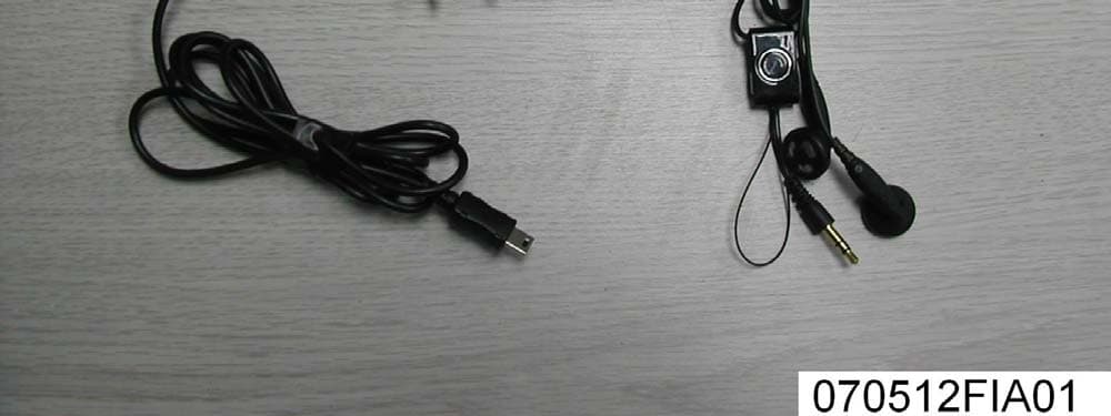
RR7BTH-012
Jul 02, 2007Stereo Bluetooth Headset
Equipment Class
DSS - Part 15 Spread Spectrum Transmitter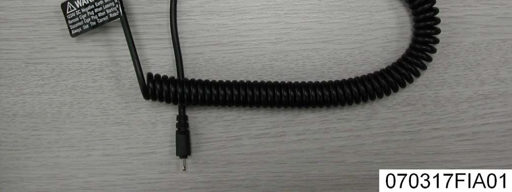
RR7GPS-005
Apr 09, 2007Bluetooth GPS Receiver
Equipment Class
DSS - Part 15 Spread Spectrum Transmitter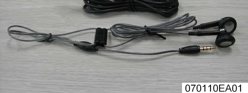
RR7BT-019
Feb 28, 2007Bluetooth Headset
Equipment Class
DSS - Part 15 Spread Spectrum Transmitter