SELTSM401SINGLE BAND CDMA MOBILE PHONE
Vitelcom Mobile Technology USA, Inc.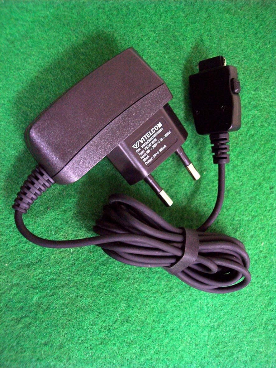
Click to zoom
Application Details
- Equipment Class
- TNE - Licensed Non-Broadcast Transmitter Held to Ear
- Date of Grant
- Dec 28, 2005
- Application Purpose
- Original Equipment
- Date of Application
- Dec 28, 2005
- Equipment Note
- SINGLE BAND CDMA MOBILE PHONE
- Frequency Range
- 824.70000000 - 848.31000000
- Country
- United States
Documents & Files
Document Text
Text extracted from the exhibit documents filed with the FCC. Open a document above to read the original.
Users Manual
CV340 User Manual Version 1.0 Prepared by: David Park Approved by: C.S.Hong Version: 1.0 Date: 12/Dec/05 -1- Revision History Version Date Pages Changes Signatures 1.0 12/Dec/05 First Version -2- Contents HEALTH AND SAFETY INFORMATION............................................................................................................6 EXPOSURE TO RADIO FREQUENCY (RF) SIGNALS..................................................................................................6 FOR BODY OPERATION...................................................................................................................................................7 DESCRIPTION FOR INDICATORS ON SCREEN AND KEYPAD............................................................8 IDLE SCREEN.....................................................................................................................................................................8 KEY LAYOUT......................................................................................................................................................................9 GETTING STARTED..................................................................................................................................................10 TURNING ON / OFF THE PHONE................................................................................................................................10 MAKING A CALL..............................................................................................................................................................10 ANSWERING A CALL.......................................................................................................................................................11 ADJUSTING VOLUME.....................................................................................................................................................11 VIEWING MISSED CALLS.............................................................................................................................................11 QUICKLY SWITCHING TO MANNER MODE.................................................................................................................12 ENTERING TEXT..............................................................................................................................................................12 USING THE MENUS.................................................................................................................................................16 ACCESSING MENU FUNCTIONS BY SCROLLING.......................................................................................................16 USING SHORTCUTS TO ACCESS MENU FUNCTIONS................................................................................................16 LIST OF MENU FUNCTIONS..........................................................................................................................................16 INTERACTIVO............................................................................................................................................................21 WAP.................................................................................................................................................................................22 ACCESSING THE WAP BROWSER..............................................................................................................................22 MY FOTO.......................................................................................................................................................................23 COMPOSE.........................................................................................................................................................................23 NOTIFICATIONS.............................................................................................................................................................23 -3- INBOX...............................................................................................................................................................................23 OUTBOX............................................................................................................................................................................23 DRAFT...............................................................................................................................................................................23 TEMPLATE........................................................................................................................................................................23 VOICE MAIL................................................................................................................................................................24 TONES & IMAGES.....................................................................................................................................................25 TONES...............................................................................................................................................................................25 IMAGES.............................................................................................................................................................................25 TORPEDO SMS...........................................................................................................................................................26 SEND MESSAGE..............................................................................................................................................................26 INBOX............................................................................................................................................…
Text truncated - open the document above for the full version.
Block Diagram
Ext e r n a l I/ O Du p lex er R F T 6122 (1 9 . 2 M H z ) P M 6610 (1 9 . 2 M H z ) TC XO ( 19. 2M H z ) M S M 6025 C a m e r a ( 3 00K ) + Back en d I C ( M V 3 0 18S O K ) ( 24. 0M H z ) LC D ( 128* 128, 65K , 1.4 1 in c h C S T N ) MC P (1 2 8 M b i t s N o r F l a s h + 32 M b i t s S R A M ) So und US B JT A G UA R T Key p ad Vi b a r a t o r RF R6 1 2 2 (1 9 . 2 M H z ) A N T E NNA Rx : 86 9- 8 9 4 M H z Tx : 824 - 8 49 M H z Po w e r A m p l if ier LED RF R x S A W RF T x S A W V d d 2. 6V V d d 2. 6V V d d 2 . 8/ 1. 8 V V d d 2. 8V 19. 2M H z 48. 0M H z 32. 768K H z 19. 2M H z
Cover Letter(s)
December 8, 2005 Vitelcom Mobile Technology U.S.A.. 2480 Irvine Boulevard, #172 Tustin, California 92782 Federal Communications Commission Authorization and Evaluation Division Confidentiality Request regarding application for certification of FCC ID: CV340_VTL401 Pursuant to Sections 0.457 and 0.459 of the Commission’s Rules, we hereby request confidential treatment of information accompanying this application as outlined below: Schematic Diagram The above materials contain trade secrets and proprietary information not customarily released to the public. The public disclosure of these materials may be harmful to the applicant and provide unjustified benefits to its competitors. The applicant understands that pursuant to Section 0.457 of the Rules, disclosure of this application and all accompanying documentation will not be made before the date of the Grant for this application. Sincerely, NAME: Monika Hormaza TITLE: Engineering Project Manager
External Photos
Test Report No.: NK2FR245 APPENDIX C – EUT PHOTOGRAPHS ● Front View of EUT Vitelcom Mobile Technology,U.S.A. Inc. FCC ID :SELTSM401 Test Report No.: NK2FR245 ● Rear View of EUT Vitelcom Mobile Technology,U.S.A. Inc. FCC ID :SELTSM401 Test Report No.: NK2FR245 ● Right Side View of EUT Vitelcom Mobile Technology,U.S.A. Inc. FCC ID :SELTSM401 Test Report No.: NK2FR245 ● Left Side View of EUT Vitelcom Mobile Technology,U.S.A. Inc. FCC ID :SELTSM401 Test Report No.: NK2FR245 ● Top View of EUT Vitelcom Mobile Technology,U.S.A. Inc. FCC ID :SELTSM401 Test Report No.: NK2FR245 ● Bottom View of EUT Vitelcom Mobile Technology,U.S.A. Inc. FCC ID :SELTSM401 Test Report No.: NK2FR245 ● Label View of EUT Vitelcom Mobile Technology,U.S.A. Inc. FCC ID :SELTSM401 Test Report No.: NK2FR245 ● Adaptor View of EUT Vitelcom Mobile Technology,U.S.A. Inc. FCC ID :SELTSM401
ID Label/Location Info
Test Report No.: NK2FR245 APPENDIX A - Labelling Requirement The sample label shown shall be permanently affixed at a conspicuous location on the device and be readily visible to the user at the time of purchase. Vitelcom Mobile Technology S.A |||||||||||||||||||||||||||||||||||||||||||||||||| ESN DEC: Decimal Made in Spain Serial No Model No.: CV340 ESN HEX: Hexadecimal FCC ID: SELTSM401 |||||||||||||||||||||||||||||||||||||||||||||||||| . L Preferred Dimension (16 (L) x 32 (W) x 0.5 (H) mm ) Optional Dimension Less than (38 (L) x 32 (W) x 0.5 (H) mm ) Vitelcom Mobile Technology,U.S.A. Inc. FCC ID :SELTSM401
Internal Photos
Test Report No.: NK2FR245 APPENDIX C – EUT PHOTOGRAPHS ● Front View of Main Board Vitelcom Mobile Technology,U.S.A. Inc. FCC ID :SELTSM401 Test Report No.: NK2FR245 ● Rear View of Main Board Vitelcom Mobile Technology,U.S.A. Inc. FCC ID :SELTSM401 Test Report No.: NK2FR245 ● Rear View of Main Board (Open Shield) Vitelcom Mobile Technology,U.S.A. Inc. FCC ID :SELTSM401
Operational Description
1. HW Feature Table1.1 HW Feature Item Description Remark Modem Qualcomm MSM6025 Packet data rates of 153 kbps on the forward and reverse links RF chip RFT6122+RFR6122+RF PAM+19.2MHz TCXO PMU PM6610 LCD 1. 128*128pixels CSTN, Transflective type 2. 65K colors 3. Solomon SSD1779Z Driver 4. 1.41inch Antenna Internal type Memory Silicon7 SV6C2832UTA 1. 128Mbits Nor-Flash 2. 32Mbits SRAM Camera 1. Sensor 300K -. HV7131RP-FB-SD74 2. Camera backend chip -. MV3018SOK External I/F 1. UART for DM 2. USB for Data service 3. Hands-Free (analog mode) 4. Travel Adapter 5. JTAG for Development Travel adapter 1. Input AC 100 ~ 240V, 50 ~ 60Hz 2. Output DC 5V, 500mA Other Shield CAN Usage 1 2. System block diagram Rx : 869-894 MHz Tx : 824-849 MHz External I/O Duplexer RFT6122 PM6610 TCXO (19.2MHz) MSM6025 Camera (300K) + Backend IC (MV3018SOK) LCD (128*128, 65K, 1.41 inch CSTN) MCP (128M bits Nor Flash + 32M bits SRAM) Sound USB JTAG UART Keypad Vibarator RFR6122 ANTENNA Power Amplifier LED 2 F IG.2-1 SYSTEM BLOCK DIAGRAM 3. SYSTEM OVERVIEW 3.1 Description of HW Circuitry 3.1.1 MSM6025 1. radioOne architecture 2. CDMA2000 1X support, offering data rates up to 153kbps on the forward and reverse links 3. Vocoder support (EVRC) 4. Integrated wideband mono voice CODEC 5. Voice recognition (VR) 6. Acoustic echo cancellation 7. External stereo DAC support 8. CMX (text, picture, and MIDI streaming) 3.1.2 PM6610 1. Power management, housekeeping, and user interface functions 2. Input power management A. Valid external supply attachment and removal detection B. Supports unregulated external charger supplies C. Supports lithium-ion main batteries D. Constant current, constant voltage, and pulse charging E. Battery voltage detectors with programmable thresholds F. Charger current regulation and real-time monitoring G. Charger transistor protection by power limit control H. Control driver for an external pass transistor I. Voltage, current, and power control loops 3. Output voltage regulation A. Seven low dropout regulator circuits with programmable output voltages, implemented using two different current ratings: 150 mA (six) and 50 mA (one). These can be used to power MSMP, MSMC, MSMA, RUIM, RFRX, RFTX, and TCXO circuits. B. Supports dynamic voltage scaling (DVS) for MSMC 3 C. All regulators can be individually enabled/disabled for power savings D. All regulated outputs are derived from a common bandgap reference – close tracking 4. Integrated handset-level user interface 5. IC-level interfaces A. MSM-compatible 3-line serial bus interface for efficient initialization, status, and control B. Supports the MSM interrupt processing with an internal interrupt manager C. Many functions monitored and reported through real-time and interrupt status signals D. Dedicated circuits for controlled power-on sequencing, including the MSM reset signal E. Several events continuously monitored for triggering power-on/power-off sequences F. Supports and orchestrates soft resets 3.1.3 RFR6122 F IG.3-1 RFR6122 IC FUCTIONAL BLOCK DIAGRAM 1. This model use QUALCOMM’s radioOne CMOS RF chipset that eliminates receive and transmit intermediate frequencies.(zero IF Support) 2. This chip is optimized for single-band, single-mode operation: Cellular-CDMA 3. Supports CDMA2000 1X and CDMA2000 1X EV-DO modes 4. Suitable for receive diversity applications that requires two RFRs and antennas. 5. Full downconversion from RF to analog baseband. 6. RF amplifiers (LNA) with Stepped gain control function are implemented. 4 7. RF-to-baseband quadrature downconverters 8. Lowpass filters, baseband amplifiers 9. Rx LO generation (UHF VCO) except receiver PLL 10. Receiver VCO is locked by other IC’s PLL ( included in RFT6122 in this model) 11. Power reduction features control extends handset standby time 12. Low power supply voltage (2.5 to 2.8 V), low power dissipation 3.1.4.RFT6122 F IG.3-2 RFT6122 IC FUCTIONAL BLOCK DIAGRAM 1. This model use QUALCOMM’s radioOne CMOS RF chipset that eliminates receive and transmit intermediate frequencies. 2. This chip is designed to support for single-band, single-mode operation: Cellular-CDMA 3. Supports CDMA2000 1X and CDMA2000 1X EV-DO modes 4. Full upconversion from analog baseband to RF 5. Transmit signal path circuits A. Baseband amplifiers B. Baseband-to-RF quadrature upconverters 5 C. RF AGC amplifiers and driver amplifiers 6. Supports all handset LO sources A. Tx synthesizer (on-chip VCO and PLL circuits) B. Rx PLL circuit 7. RF AGC Amplifier have greater than 85-dB transmit power control range. 8. Power reduction features via MSM control extends handset talk-time A. Optimized for low DC power consumption versus RF output power level B. Transmit puncturing C. Selective circuit power-down D. Gain control 9. Low power supply voltage (2.5 to 2.8 V), low power dissipation 3.2 MSM6025’s Memory Interface In the MSM6025 device, the external memory interface is upgraded to support page mode memories and NAND flash memories, and allows access to external memories by the ADSP QDSP4 processor. The ADSP uses the direct memory exchange (DME) interface for that purpose. 1. Interface support for generic (asynchronous interface) NOR FLASH and SRAM devices 2. Interface support for byte addressable 16-bit devices (ub_n and lb_n signals) 3. Interface support for 8-bit devices on SRAM0, SRAM1, GP0 and GP1 chip selects 4. Interface support for page mode memories on all chip selects (with the exception of LCD) 5. Programmable first access wait state for page mode memories 6. Interface support for some Pseudo-Static types of RAM by means of a programmable address to cs_n setup time 7. Programmable recovery/turnover wait states for each cs_n 8. Programmable and separate write access and read access wait states for each cs_n 3.2.1 Access Types In the MSM6025 AHB system, three different transfer sizes can be attempted: WORD(32bits), HWORD(16bits), and BYTE transfers. Table 3.2.1 Access Type by chip select 6 Chip Select 32x16 16 8ubx16 …
Text truncated - open the document above for the full version.
Parts List/Tune Up Info
REF-DES Description Qty Manufacturer PART NUMBER SIZE Value VITELCOM P/N D1 RF Schottky Barrier Diodes 1 Agilent HMPS-2822 HMPS-2822 VMTDD000450141207 U4 Charge Pump for White LED 1 Analogic Tech AAT3113ITP-20-TI AAT3113ITP-20-TI VMTICS00690TSOP12 CON4 32pin LCD connector 1 DDK FF14-32C-R16B FF14-32C-R16B VMTCNS0047000032P VRS9-20 VARISTOR,10PF,18V,1005 12 ICT ICVL0518100Y500 1005 10PF VMTVAR00160000402 VRS22-24 VRS26-27 VRS30VRS34-36 VARISTOR,360PF,5.6V,1005 9 ICT ICVN0505X150 1005 360PF VMTVAR00230000402 VRS21 VRS28 VRS31 VARISTOR,480PF,5.6V,1005 3 ICT ICVS0505481 1005 480PF VMTVAR00270000402 VRS32-33 VARISTOR,550PF,9V,1608 2 ICT ICVN1009A200 1608 550PF VMTVAR00240000603 VRS40-44 VARISTOR,60PF,5.6V,1005 5 ICT ICVL0505600V150 1005 60PF VMTVAR00260000402 OSC1 X-TAL, 32.768KHZ,4.1*1.5 1 KDS DST410 4.1*1.5 32.768KHZ VMTCRS00160154107 Q2 TCXO, 19.2MHz 1 KDS DSA321SA DSA321SA VMTCRS00320322509 D2 D4 Switching Diode EMD2 Type 2 KEC KDS160E ESC KDS160E VMTDD00047000ESC2 Q6 GENERAL AMP, PNP 1 KEC KTA1532T TSM KTA1532T VMTTR00046000TSM3 Q4 GENERAL AMP, PNP 1 KEC KTA2012E ESM KTA2012E VMTTR00047000ESM3 Q5 GENERAL AMP, NPN 1 KEC KTC4072E ESM KTC4072E VMTTR00048000ESM3 Q108 NPN POWER TRANSISTOR,UMT3 1 KEC KTN2222AU UMT3 KTN2222AU VMTTR000340000USM U5 SMD type Microphone 1 KNOWLES SP0102NC3-3 SP0102NC3-3 VMTPZU0011A000MIC L8 IC,EMIFILTER,0.05OHM,2A,2012 1 MARUWA CNH20F104Z-TM 2012 CNH20F104Z-TM VMTIND00880000805 U116 IC,150mA CMOS LDO,SC70 1 MICRO CHIPS TC1017-2.85V SC70 LDO-2.85V VMTREG001800SC705 U21 Camera IC 1 MTekvision MV3018SOK MV3018SOK VMTICS0252CABGA81 U100 RF SWITCH 1 MURATA MM8430-2600RB3 MM8430-2600RB3 VMTCNS0029000002P U16 RF Tx SAW Filter 5pin Unbalance type 1 MURATA SAFEB836MAL0F00 1.4*1.1*0.6 SAFEB836MAL0F00 VMTFTS00570131006 U18 RF Rx SAW Filter 5pin Balance type 1 MURATA SAFEB881MFM0F00 1.4*1.1*0.6 SAFEB881MFM0F00 VMTFTS00580131006 U13 SAW Duplxer 1 MURATA SAYDV836MAB0F00R05 SAYDV836MAB0F00R05 VMTFTS00590383812 R151 THERMISTOR,CHIP,150k,±5%,2.8mw/K,0805 1 MURATA NCP18WM154J03RB 603 THERMISTOR VMTNTC00050000603 U12 AUDIO AMP 1 NATIONALSEMICONDUCTOR LM4898LD_LLP LLP LM4898LD_LLP VMTICS00920LDA10B L4 L16 INDUCSM,CHIP, 10NH,±5%, 250mA,1005 2 PILKOR 1005GC2T10NJ00 1005 10NH VMTIND00770000402 L11 INDUCSM,CHIP, 120NH,±5%, 250mA,1005 1 PILKOR 1005GC2T121NJ00 1005 120NH VMTIND00350000402 L12 L14-15 INDUCSM,CHIP, 2.7NH ±0.3nH,0.22OHM,300mA,1005 3 PILKOR 1005GC2T2N7S00 1005 2.7NH VMTIND00380000402 L13 L20 L23 INDUCSM , CHIP , 47NH , ± 5% 0 31OHM 600mA 1005 3 PILKOR 1005GC2T47N#00 1005 47NH VMTIND00530000402 L17 INDUCSM , CHIP , 8 . 2NH , ± 5% 0 31OHM 600mA 1005 1 PILKOR 1005GC2T8N2#00 1005 8.2NH VMTIND00760000402 L3 L5 INDUCSM , CHIP , 82NH , ± 5% 1 2OHM 150mA 1005 2 PILKOR LQG15HS82NJ02D 1005 82NH VMTIND01190000402 U2 MSM6025 Digital-Baseband 1 Qualcomm MSM6025 MSM6025 VMTICS0222FBGA208 U7 POWER MANAGEMENT IC 1 Qualcomm PM6610 PM6610 VMTICS022300QFN32 U6 Rx ZIF chip 1 Qualcomm RFR6122 RFR6122 VMTICS022400QFN32 U10 Tx ZIF Chip 1 Qualcomm RFT6122 RFT6122 VMTICS022500QFN32 R2 R4-8 R10 R20 R36-40 R42-44 R61 R69 R71-72 R86 R122R206-213 R215 RESSM,CHIP,0R,±5%,0.1W,1005 31 ROHM RMC1/16S000JTH 1005 0R VMTRS000140000402 R27 R88 RESSM,CHIP,100K,±5%,0.1W,1005 2 ROHM RMC1/16S104JTH 1005 100K VMTRS000110000402 R17 RESSM,CHIP,100m,±1%,0.1W,1608 1 ROHM RMC1/16S100mFTH 1608 100m ±1% VMTRS001560000603 R15 R30 R60 R64 RESSM,CHIP,100R,±5%,0.1W,1005 4 ROHM RMC1/16S101JTH 1005 100R VMTRS000350000402 R11-12 R16 R18 R28 R32 R56-57 R59 R73 R76 R94R24 R63 R110-111 RESSM,CHIP,10K,±5%,0.1W,1005 RESSM,CHIP,10R,±5%,0.1W,1005 12 4 ROHM ROHM RMC1/16S103JTH RMC1/16S100JTH 1005 1005 10K 10R VMTRS000100000402 VMTRS000050000402 R34 RESSM,CHIP,11.8K,±1%,0.1W,1005 1 ROHM RMC1/16S1182FTH 1005 11.8K ±1% VMTRS001510000402 R99 RESSM,CHIP,121K,±1%,0.1W,1005 1 ROHM RMC1/16S1213FTH 1005 121K ±1% VMTRS001270000402 R112 R114 RESSM,CHIP,180K,±5%,0.1W,1005 2 ROHM RMC1/16S184JTH 1005 180K VMTRS001110000402 R13 R22 R25-26 R31 R96-98 RESSM,CHIP,1K,±5%,0.1W,1005 8 ROHM RMC1/16S102JTH 1005 1K VMTRS000250000402 R9 R109 RESSM,CHIP,1M,±5%,0.1W,1005 2 ROHM RMC1/16S105JTH 1005 1M VMTRS000210000402 R14 R133 RESSM,CHIP,1R,±5%,0.1W,1005 2 ROHM RMC1/16S010JTH 1005 1R VMTRS000340000402 R104 R116 RESSM,CHIP,2.2K,±5%,0.1W,1005 2 ROHM RMC1/16S222JTH 1005 2.2K VMTRS000240000402 R67 RESSM,CHIP,2.7K,±5%,0.1W,1005 1 ROHM RMC1/16S272JTH 1005 2.7K VMTRS000120000402 R100 RESSM,CHIP,200R,±5%,0.1W,1005 1 ROHM RMC1/16S201JTH 1005 200R VMTRS000790000402 R45-46 R65-66 RESSM,CHIP,20K,±1%,0.1W,1005 4 ROHM RMC1/16S2002FTH 1005 20K ±1% VMTRS000750000402 R103 RESSM,CHIP,22K,±5%,0.1W,1005 1 ROHM RMC1/16S223JTH 1005 22K VMTRS000410000402 R105 RESSM,CHIP,22K,±1%,0.1W,1005 1 ROHM RMC1/16S2202FTH 1005 22K ±1% VMTRS001520000402 R21 RESSM,CHIP,3.3K,±1%,0.1W,1005 1 ROHM RMC1/16S3301FTH 1005 3.3K ±1% VMTRS000760000402 R48 RESSM,CHIP,3K,±1%,0.1W,1005 1 ROHM RMC1/16S302FTH 1005 3K ±1% VMTRS001540000402 R1 R3 RESSM,CHIP,4.7K,±5%,0.1W,1005 2 ROHM RMC1/16S472JTH 1005 4.7K VMTRS000470000402 R58 R70 RESSM,CHIP,4.7R,±5%,0.1W,1005 2 ROHM RMC1/16S4R7JTH 1005 4.7R VMTRS000610000402 R150 RESSM,CHIP,470K,±1%,0.1W,1005 1 ROHM RMC1/16S474FTH 1005 470K ±1% VMTRS001090000402 R41 R49 R52 R80-82 R84-85R87 RESSM,CHIP,470R,±5%,0.1W,1005 9 ROHM RMC1/16S471JTH 1005 470R VMTRS000460000402 R101-102 R106 R123 RESSM,CHIP,47K,±5%,0.1W,1005 4 ROHM RMC1/16S473JTH 1005 47K VMTRS000270000402 R55 R113 RESSM,CHIP,510K,±5%,0.1W,1005 2 ROHM RMC1/16S514JTH 1005 510K VMTRS001120000402 R51 R53 R221-223 RESSM,CHIP,51R,±5%,0.1W,1005 5 ROHM RMC1/16S510JTH 1005 51R VMTRS00007000402 R50 R227 RESSM,CHIP,6.2K,±5%,0.1W,1005 2 ROHM RMC1/16S622JTH 1005 6.2K VMTRS000130000402 R33 RESSM,CHIP,7.5K,±5%,0.1W,1005 1 ROHM RMC1/16S752JTH 1005 7.5K VMTRS001130000402 R149 RESSM,CHIP,80.6K,±1%,0.1W,1005 1 ROHM RMC1/16S8062FTH 1005 80.6K ±1% VMTRS001040000402 R23 RESSM,CHIP,82R,±5%,0.1W,1005 1 ROHM RMC1/16S820JTH 1005 82R VMTRS001230000402 U1 USB TRANSCEIVER,16-PIN MLF 1 SAMSUNG S1M8720X 16-LPCC S1M8720X VMTICS02260LPCC16 L2 L7 BEAD,FERRITE…
Text truncated - open the document above for the full version.
Parts List/Tune Up Info
Test Report No.: NK2FR245 APPENDIX H – TUNE UP PROCEDURE Vitelcom Mobile Technology,U.S.A. Inc. FCC ID :SELTSM401 Test Report No.: NK2FR245 Test Configuration of Equipment under Test The EUT has been tested under continuous transmitting mode. All tests are performed at Low channel , Middle channel, High channel. The field strength of spurious radiation emission for CDMA was measured at EUT stand-up position (H mode) and lie down position (E1 , E2 mode). During all testings, EUT is in link mode with Base Station emulator (8960 Series 10) at maximum power level. Frequency range has been investigated : Radiated emission has been measured from 30MHz to 12.75GHz. Vitelcom Mobile Technology,U.S.A. Inc. FCC ID :SELTSM401
RF Exposure Info
SAR Report Reference No.: NK2FR246 SAR Evaluation Report FCC ID : SELTSM401 Project Reference No. : NK2FR246 Product Type : Single Band CDMA Mobile Phone Brand Name : Sacar Model : CV340_VTL401 Tested According to : IEEE Standard C95.1 / OET Bulletin 65 Supplement C Tested Period : December. 12. 2005 to December. 16. 2005 Tested by Seob.Lee date : December. 19. 2005 Verified by Seonteag.Jin date : December. 19. 2005 This test results are only related to the item tested. This test report is only limited to the client company and the product. This report must not be used by the client to claim product endorsement by any agency of the U.S. Government. Lab Address : Nemko Korea Co., Ltd 300-2, Osan-Ri, Mohyun-Myun, Yongin-City, Gyunggi-Do, Korea Phone : 82-31-322-2333 Fax : 82-31-322-2332 Vitelcom Mobile Technology USA,Inc Page 1 of 58 FCC ID : SELTSM401 SAR Report Reference No.: NK2FR246 Contents of This Report 1. General Information 3 1.1 Applicant 3 1.2 Manufacturer 3 1.3 Description of Device 3 2. General Test Condition 4 2.1 Location 4 2.2 Operating Environment 4 2.3 Test Frequency 4 2.4 Support Equipment 4 3. Description of Test Equipment 5-9 4. SAR Measurement Procedure 9 5. Definition of Reference Points 11 5.1 Ear Reference Point 11 5.2 Handset Reference Points 12 6. Test Configuration Positions 13 6.1 Cheek/Touch Position 13 6.2 Ear/Tilt 15Position 14 6.3 Body-worn and Other Configurations 15 7. Measurement Uncertainty 16 8. System Verification 17 8.1 Tissue Verification 17 8.2 Test System Validation 18 8.3 Measurement Result of Test Data (Head Validation) 19 8.4 Measurement Result of Test Data (Muscle Validation) 20 9. SAR Measurement Results 21-22 9.1 SAR Measurement Result(Right Head Touch Position) 23-26 9.2 SAR Measurement Result (Right Head Tilt Position) 27-28 9.3 SAR Measurement Result (Left Head Touch Position) 29-32 9.4 SAR Measurement Result (Left Head Tilt Position) 33-34 9.5 SAR Measurement Result (Muscle–15mm Distance- Position) 35-38 9.6 SAR Measurement Result (Muscle–15mm Distance- with Headset) 39-40 10. SAR Test Equipment 41 11. References 42 Appendix A SAR Definition 43-44 Appendix B Probe Calibration 45-53 Appendix C Probe Interpolation 54 Appendix D Photographs of EUT 55-58 Vitelcom Mobile Technology USA,Inc Page 2 of 58 FCC ID : SELTSM401 SAR Report Reference No.: NK2FR246 1.General Information 1.1 Applicant Company Name: Vitelcom Mobile Technology,U.S.A. Inc. Company Address: 2480 Irvine Boulevard #172 Tustin, CA 92782 U.S.A Phone/Fax: Phone: 714-389-1169 Contact Name: Monika Hormaza 1.2 Manufacturer Company Name: Vitelcom Mobile Technology,SA. Company Address: Avenada Juan Lopez Penalver 37 Malaga, Spain,29590 Phone/Fax: Phone: 714-389-1169 Contact Name: Monika Hormaza 1.3 Description of Device Category: Single Band CDMA Mobile Phone Model Name: CV340_VTL401 Brand Name: Sacar Serial Number: 0000001 Frequency of Operation Tx : 824MHz ~ 849MHz, Rx : 869MHz ~ 894MHz RF Output Power (Conducted) 23.5dBm Modulation/Demodulation OQPSK/QPSK Channel Spacing 1.23MHz Receiver Sensitivity -104dBm Operating Condition -20 to +60 Power Supply Li-ion Battery: 3.7V DC, 650mAh Phone Type Bar Type Antenna Type Internal Dimensions 100.0(H) X44.0(V) X 16.4(T)mm Weight 68g(with Battery) Remarks: - Vitelcom Mobile Technology USA,Inc Page 3 of 58 FCC ID : SELTSM401 SAR Report Reference No.: NK2FR246 2. General Test Condition 2.1 Location Nemko Korea 300-2, Osan-Ri, Mohyun-Myun, Yongin-City, Gyunggi-Do Phone : 82-31-322-2333 , Fax : 82-31-322-2332 2.2 Operating Environment Parameters Recording during test Accepted deviation Ambient temperature 20 ~22 15 ~ 30 Relative humidity 30 ~60% 20 ~ 75% 2.3 Test Frequency CDMA (Head) CDMA ( Muscle) Test Channel Test Frequency (MHz)Test Channel Test Frequency (MHz) 1013 824.70 1013 824.70 363 835.89 363 835.89 777 848.31 777 848.31 2.4 Support Equipment Equipment Manufacturer Model Name Serial Number - - - - Vitelcom Mobile Technology USA,Inc Page 4 of 58 FCC ID : SELTSM401 SAR Report Reference No.: NK2FR246 3. Description of Test Equipment 3.1 SAR Measurement Setup Robotic System Measurements are performed using the DASY4 automated dosimetric assessment system. Which is made by Schmid & Partner Engineering AG (SPEAG) in Zurich, Switzerland and consists of high precision robotics system (Stäubli), robot controller, measurement server, H/P computer, nearfield probe, probe alignment sensor, and the SAM twin phantom containing the brain equivalent material. The robot is a six-axis industrial robot performing precise movements to position the probe to the location (points) of maximum electromagnetic field (EMF) (see Fig. 3.1). Figure 3.1 SAR Measurement System Setup System Hardware A cell controller system contains the power supply, robot controller, teach pendant (Joystick), and a remote control is used to drive the robot motors. The PC consists of the H/P computer with Windows XP system and SAR Measurement Software DASY4, LCD monitor, mouse and keyboard. The Stäubli Robot is connected to the cell controller to allow software manipulation of the robot. A Data Acquisition Electronic (DAE) circuit that performs the signal amplification, signal multiplexing, AD-conversion, offset measurements, mechanical surface detection, collision detection, etc. Is connected to the Electro-Optical Coupler (EOC). The EOC performs the conversion from the optical into digital electric signal of the DAE and transfers data to the measurement server. Vitelcom Mobile Technology USA,Inc Page 5 of 58 FCC ID : SELTSM401 SAR Report Reference No.: NK2FR246 System Electronics The DAE4 consists of a highly sensitive electrometer-grade preamplifier with autozeroing, a channel and gain-switching multiplexer, a fast 16-bit AD-converter and a command decoder and control logic unit. Transmission to the measurement server is accomplished through an optical downlink for data and status information and an optical uplink for commands and clock lines. The mechanical probe mounting device…
Text truncated - open the document above for the full version.
Test Report
Test Report No.: NK2FR245 Vitelcom Mobile Technology,U.S.A. Inc. FCC ID :SELTSM401 Page 1 of 51 Nemko Korea CO., Ltd. 300-2, Osan-Ri, Mohyun-Myun, Yongin-City, Gyunggi-Do, KOREA TEL:+82 31 322 2333 FAX:+82 31 322 2332 FCC EVALUATION REPORT FOR CERTIFICATION Applicant : Vitelcom Mobile Technology,U.S.A. Inc. Dates of Issue : December, 27, 2005 2480 Irvine Boulevard #172 Test Report No. : NK2FR245 Tustin,CA 92782 U.S.A Test Site : Nemko Korea Co., Ltd. FCC ID Brand Name CONTACT PERSON Applied Standard: FCC 47 CFR Part 22H & Part 2 Test Procedure: ANSI C63.4 , TIA/EIA 603 Equipment Class: Public Mobile Services EUT Type: Single Band CDMA Mobile Phone The device bearing the brand name and FCC ID specified above has been shown to comply with the applicable technical standards as indicated in the measurement report and was tested in accordance with the measurement procedures specified in ANSI C63.4-2003. I attest to the accuracy of data and all measurements reported herein were performed by me or were made under my supervision and are correct to the best of my knowledge and belief. I assume full responsibility for the completeness of these measurements and vouch for the qualifications of all persons taking them. Tested By : S. Lee Reviewed By : H.H. Kim Engineer Manager & Chief Engineer SELTSM401 Sacar Bellwave Co., Ltd. 2480 Irvine Boulevard #172 Tustine,CA 92782 U.S.A Mr. Monika Hormaza Telephone No. :714-389-1169 Test Report No.: NK2FR245 Vitelcom Mobile Technology,U.S.A. Inc. FCC ID :SELTSM401 Page 2 of 51 TABLE OF CONTENTS 1. SCOPE 2. INTRODUCTION (Site Description) 3. TEST CONDITIONS & EUT INFORMATION 4. MEASURING INSTRUMENT CALIBRATION 5. SUMMARY OF TEST RESULTS 6. TEST EQUIPMENT 7. DESCRIPTION OF TEST 7.1 Conducted Emissions 7.2 Radiated Emissions 7.3 Effective Radiated Power/Equivalent Isotropic Radiated Power 7.4 Radiated Spurious & Harmonic E…
Text truncated - open the document above for the full version.
Contact Information
Applicant
Monika Hormaza(Engineering Project Manager)
Test Firm
Nemko Korea Co., LtdHyun Kim
Technical Specifications
| # | Rule Parts | Frequency Range | Power Output | Emission | Tolerance |
|---|---|---|---|---|---|
| 1 | 22H | 824.7 MHz - 848.31 MHz | 490.00 mW | 1M25F9W | 2.5000000000 ppm |
Other Applications from Vitelcom Mobile Technology USA, Inc.
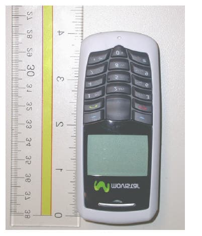
SELTSM102
Mar 02, 2006CDMA Phone
Equipment Class
TNE - Licensed Non-Broadcast Transmitter Held to Ear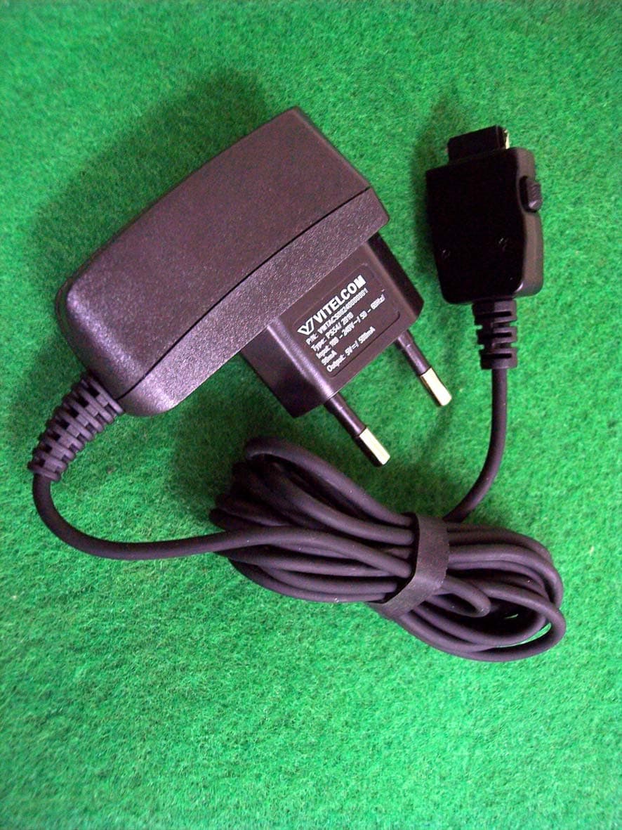
SELTSM601
Dec 28, 2005Single Band CDMA Mobile Phone
Equipment Class
TNE - Licensed Non-Broadcast Transmitter Held to Ear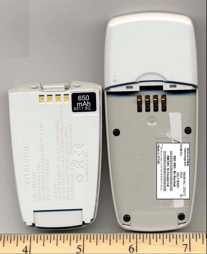
SELTSM201
Jun 13, 2005Single Band CDMA Cellular Phone
Equipment Class
TNE - Licensed Non-Broadcast Transmitter Held to Ear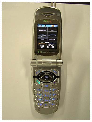
SELTSM501
May 05, 2005Single Band CDMA Cellular Phone
Equipment Class
TNE - Licensed Non-Broadcast Transmitter Held to Ear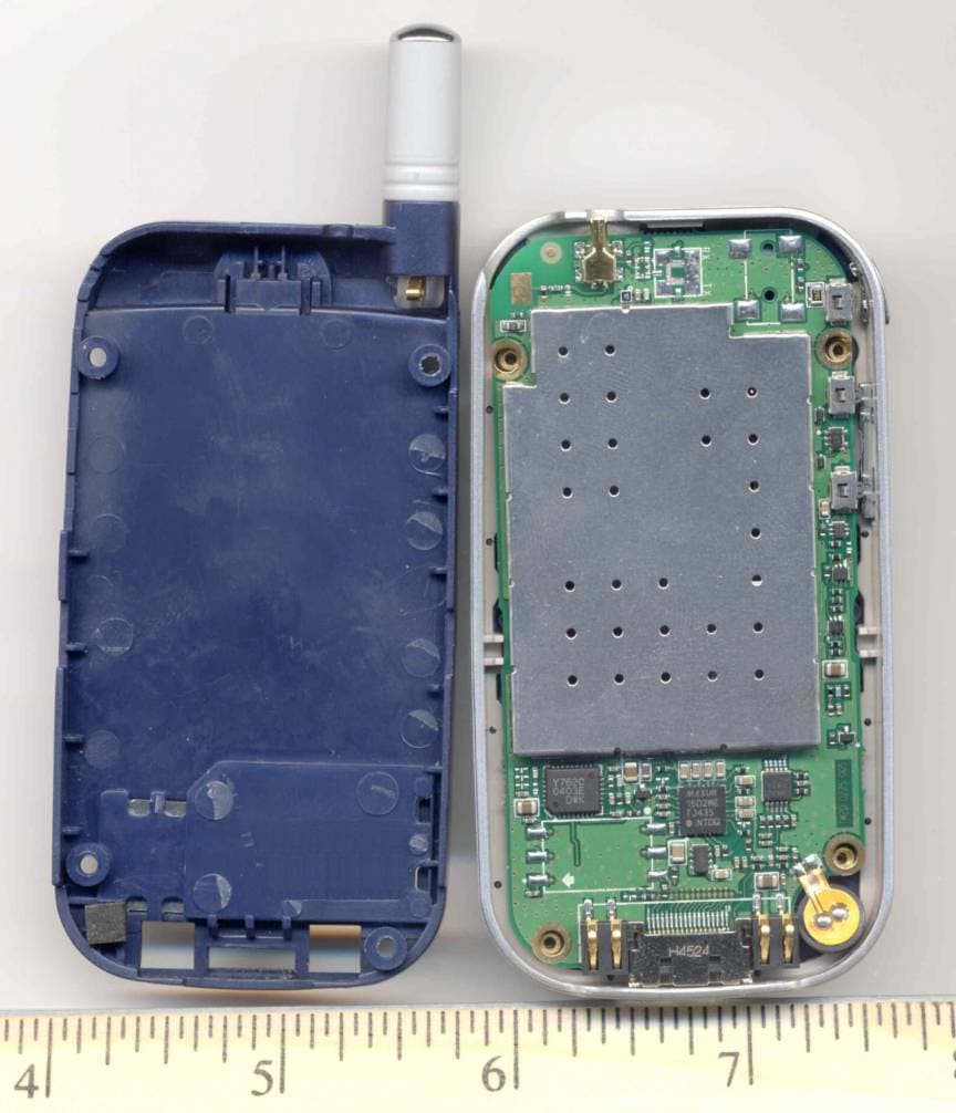
SELTSM301
Apr 13, 2005Single Band CDMA Cellular Phone
Equipment Class
TNF - Licensed Non-Broadcast Transmitter Held to Face