SMQSD6-MAINBluetooth Module
EDAN INSTRUMENTS, INC.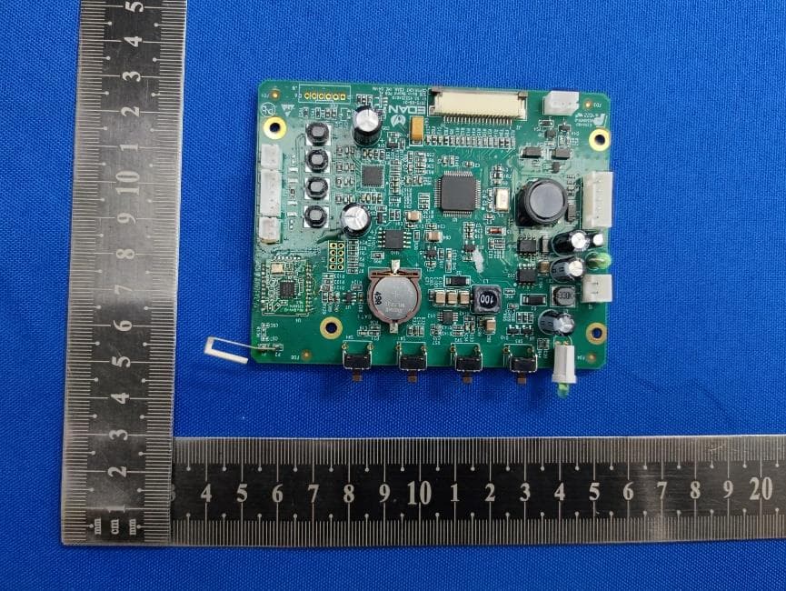
Click to zoom
Application Details
- Equipment Class
- DTS - Digital Transmission System
- Date of Grant
- Sep 26, 2023
- Application Purpose
- Original Equipment
- Date of Application
- Sep 07, 2023
- Equipment Note
- Bluetooth Module
- Frequency Range
- 2402.00000000 - 2480.00000000
- Company
- EDAN INSTRUMENTS, INC.
- Country
- China
Documents & Files
Document Text
Text extracted from the exhibit documents filed with the FCC. Open a document above to read the original.
Users Manual
1 Product Overview 1.1 Introduction The SD6 is a highly integrated Bluetooth 5.0 low energy module device. It has 32-bit ARM® Cortex™-M0 CPU with 512KB Flash, 64KB SRAM and an ultra-low power, high performance, multi-mode radio. It intergrates rich feature peripheral units, programmable protocol and profile to support BLE application, makes customers’ product to be built with minimum bill-of-material (BOM) cost. 1.2 Features 1.3 Features CPU ⚫ 32-bit ARM® Cortex™-M0 CPU ⚫ Up to 64MHz clock Memories ⚫ 512KB Flash ⚫ 64KB Data SRAM ⚫ 8KB Code Cache 2.4GHz Transceiver ⚫ Compliant to Bluetooth 5.0 ⚫ Single-pin antenna: no RF matching or RX/TX switching required ⚫ Support two data rates — 2Mbps — 1Mbps ⚫ TX Power -20 to +5dBm in 3dB steps Low power consumption ⚫ Transmitter: 5.5mA@0dBm Tx power, with DC-DC ⚫ Receiver: 5mA @with DC-DC ⚫ Sleep Mode 13μA@with 32KHz RTC and all SRAM retention ⚫ 0.7μA @ OFF Mode(IO wake up only) Oscillator ⚫ Support 16M XTAL ⚫ Embedded 32M RC oscillator and 32K RC oscillator PeriPheral ⚫ 20/9 general purpose I/O pins — All pins can be configured as digital interface by programmable IO MUX function mapping(except P01) — All pins can be configured for wake-up and external interrupt — All pins output state can be retained in sleep mode ⚫ 2x UART ⚫ 6-channel output PWM ⚫ 2x I2C ⚫ 2x SPI ⚫ 1x 12bit ADC, support 6ch or 3ch single- ended input ⚫ 1x PGA, support analog microphone input ⚫ 4ch DMA ⚫ 6x 24bit timer ⚫ WDT ⚫ SWD debug Flexible power management ⚫ Supply voltage range 1.9V to 3.6V ⚫ Embedded 1.35V buck DC-DC converter(it does not exist in SOP16 package) Package ⚫ QFN32(4*4*0.75mm) ⚫ SOP16(9.90*3.90*1.40mm) Certification ⚫ BQB:D054808 Application ⚫ Health and medical ⚫ Wearables ⚫ Internet of things (IoT) 1.3 Pin Assignments and Functions 3 / 6 This section describes the pin assignment and the pin functions for the different package types. Figure 1.1 Module pin assignments Table 1.1 Pin description item Pin name Type Description 1 GND P Ground 2 BAT_IN P 3.3V power input 3 NC / Reserved 4 NC / Reserved 5 NC / Reserved 6 NC / Reserved 7 P14/WAKEUP I/O General purpose input/output 8 P02/SWD_IO I/O General purpose input/output / SWD debug IO 9 P03/SWD_CLK I/O General purpose input/output / SWD debug CLK 10 P11/BT_STATUS I/O General purpose input/output 11 P31 I/O General purpose input/output 12 P32 I/O General purpose input/output 13 P33 I/O General purpose input/output 14 P24/BOOT1 I/O General purpose input/output 15 P25/BOOT2 O General purpose input/output 16 BOOT0 I Boot select[0], enter program mode or test mode when high level input. default pull-down 17 VDD25 I 1.35V BUCK DCDC output power feedback input, and digital 1.2V LDO input. When don’t use DC- DC, this pin should connect to VDD 18 SW_OUT O 1.35V BUCK DCDC switch output. When don’t use DCDC, this pin should be float. 19 RST_N I Reset pin input, low level active 20 P10/RXD I General purpose input/output / Debug RXD 21 P09/TXD O General purpose input/output / Debug TXD 22 P18/HCI_RXD I/O General purpose input/output / UART_RXD 23 P20/HCI_TXD I/O General purpose input/output / UART_TXD 24 P23/AIO1 I/O General purpose input/output 25 P26 I/O General purpose input/output 26 XTAL32K_IN I 32.768KHz crystal input 27 XTAL32K_OUT O 32.768KHz crystal output 28 P27 O LED1 driver 29 GND P Ground 30 BT_RF RI/O RF Port CST92F34-SOP16 4 / 6 FCC Statement This Module complies with part 15 of the FCC rules. Operation is subject to the following two conditions: (1) this module may not cause harmful interference, and (2) this module must accept any interference received, including interference that may cause undesired operation. Changes or modifications not expressly approved by the party responsible for compliance could void the user’s authority to operate the equipment. NOTE: This equipment has been tested and found to comply with the limits for a Class B digital device, pursuant to part 15 of the FCC Rules. These limits are designed to provide reasonable protection against harmful interference in a residential installation. This equipment generates uses and can radiate radio frequency energy and, if not installed and used in accordance with the instructions, may cause harmful interference to radio communications. However, there is no guarantee that interference will not occur in a particular installation. If this equipment does cause harmful interference to radio or television reception, which can be determined by turning the equipment off and on, the user is encouraged to try to correct the interference by one or more of the following measures: ‐ Reorient or relocate the receiving antenna. ‐ Increase the separation between the equipment and receiver. ‐ Connect the equipment into an outlet on a circuit different from that to which the receiver is connected. ‐Consult the dealer or an experienced radio/TV technician for help important announcement Radiation Exposure Statement The module has been evaluated to meet general RF exposure requirement. The device can be used in portable exposure condition without restriction. Important Note: In the event that these conditions cannot be met (for example certain laptop configurations or co-location with another transmitter), then the FCC authorization is no longer considered valid and the FCC ID cannot be used on the final product. In these circumstances, the OEM integrator will be responsible for re-evaluating the end product (including the transmitter) and obtaining a separate FCC authorization. End Product Labeling The final end product must be labeled in a visible area with the following" Contains FCC ID: SMQSD6-MAIN ". 5 / 6 Integration instructions for host product manufacturers according to KDB 996369 D03 OEM Manual v01r01 List of applicable FCC rules CFR 47 FCC PART 15 SUBPART C has been investigated. It is applicable to the modular transmitter. Specific operational use conditions This module is stand-alone modular. If the end product will involve the Multiple simultaneousl…
Text truncated - open the document above for the full version.
Cover Letter(s)
Edan Instruments, Inc #15 Jinhui Road, Jinsha Community, Kengzi Sub-District, Pingshan District,518122 Shenzhen P.R.China Limited Single Modular Approval Request Letter Date: July 20, 2023 To: Federal Communications Commission Authorization and Evaluation Division 7435 Oakland Mills Road Columbia, MD Subjects: Limited Single Modular Approval Request Letter The Device,FCC ID: SMQSD6-MAIN, is seeking FCC authorization as a modular transmitter. The EUT meets the requirement for modular approval as detailed in FCC Public Notice DA 00-1407. Compliance to each of the requirement is described below: (a) The radio elements must have the radio frequency circuitry be shielded. Physical/discrete and tuning capacitors may be located external to the shield, but must be on the module assembly. No, not shielded. (b) The module shall have buffered modulation/data input(s) (if such inputs are provided) to ensure that the module will comply with the requirements set out in the applicable RSS standard under conditions of excessive data rates or over-modulation. Yes. The EUT has its buffered modulation. Please see the Schematic Diagram. (c) The module shall have its own power supply regulation on the module. This is to ensure that the module will comply with the requirements set out in the applicable standard regardless of the design of the power supplying circuitry in the host device which houses the module. Yes, The modular with power management chip CST92F34. (d) The module shall comply with the provisions for external power amplifiers and antennas detailed in this standard. The equipment certification submission shall contain a detailed description of the configuration of all antennas that will be used with the module. Yes, Allowed antennas given in certification application information and manual (e) The module shall be tested for compliance with the applicable standard in a stand-alone configuration, i.e. the module must not be inside another device during testing. Yes, The EUT was tested with a test board, Please see test report and setup photo. (f) The module shall comply with the Category I equipment labeling requirements and CFR § 15.212(a)(1)(vi). Edan Instruments, Inc #15 Jinhui Road, Jinsha Community, Kengzi Sub-District, Pingshan District,518122 Shenzhen P.R.China Yes, Please see exhibition label sample for the FCC ID of this module. And also in the exhibition Users manual, there are instructions give to the OEM on how to label the end product. (g) The module shall comply with any applicable FCC RF exposure requirement which are based on the intended use/configurations. Yes,the module is intended to use in protable/mobile environment. FCC RF exposure requirement satisfied with 47CFR §2.1093. (h) The modular transmitter complies with all applicable FCC rules. Instructions for maintaining compliance are given in the user instructions. Yes, The EUT is compliant with all applicable FCC rules. Details instructions for maintaining compliance are give in the User Manual. If you have any questions, please feel free to contact us at the address shown below Sincerely, Name: Huanhuan Xia Company: Edan Instruments, Inc Address: #15 Jinhui Road, Jinsha Community, Kengzi Sub-District, Pingshan District,518122 Shenzhen P.R.China Phone: 0086 755 26682547 Fax: 0086 755 26882223 E-Mail: [email protected]
External Photos
FCC ID: SMQSD6-MAIN Bluetooth Antenna
ID Label/Location Info
FCC ID: SMQSD6-MAIN
Internal Photos
FCC ID: SMQSD6-MAIN
RF Exposure Info
RF Exposure evaluation FCC ID: SMQSD6-MAIN 1.1. Applicable Standard According to §1.1307(b)(1), systems operating under the provisions of this section shall be operated in a manner that ensures that the public is not exposed to radio frequency energy level in excess of the Commission’s guidelines. According to §1.1310 and §2.1093 RF exposure requirement KDB447498 v06: Mobile and Portable Devices RF Exposure Procedures and Equipment Authorization Policies 1.2. Requirement According to KDB447498 D01 General RF Exposure Guidance v06 Section 4.3.1 Standalone SAR test exclusion considerations: “Unless specifically required by the published RF exposure KDB procedures, standalone 1-g head or body and 10-g extremity SAR evaluation for general population exposure conditions, by measurement or numerical simulation, is not required when the corresponding SAR Test Exclusion Threshold condition, listed below, is satisfied. These test exclusion conditions are based on source-based time-averaged maximum conducted output power of the RF channel requiring evaluation, adjusted for tune-up tolerance, and the minimum test separation distance required for the exposure conditions.22 The minimum test separation distance is determined by the smallest distance from the antenna and radiating structures or outer surface of the device, according to the host form factor, exposure conditions and platform requirements, to any part of the body or extremity of a user or bystander (see 5) of section 4.1). To qualify for SAR test exclusion, the test separation distances applied must be fully explained and justified by the operating configurations and exposure conditions of the transmitter and applicable host platform requirements, typically in the SAR measurement or SAR analysis report, according to the required published RF exposure KDB procedures. When no other RF exposure testing or reporting is required, a statement of justification and compliance must be included in the equipment approval, in lieu of the SAR report, to qualify for the SAR test exclusion. When required, the device specific conditions described in the other published RF exposure KDB procedures must be satisfied before applying these SAR test exclusion provisions; for example, handheld PTT two-way radios, handsets, laptops & tablets etc.23 “ [(max. power of channel, including tune-up tolerance, mW)/ (min. test separation distance, mm)] · [√f (GHz)] ≤ 3.0 for 1-g SAR and ≤ 7.5 for 10-g extremity SAR, where: • f (GHz) is the RF channel transmit frequency in GHz • Power and distance are rounded to the nearest mW and mm before calculation • The result is rounded to one decimal place for comparison • 3.0 and 7.5 are referred to as the numeric thresholds in the step 2 below The test exclusions are applicable only when the minimum test separation distance is ≤ 50 mm and for transmission frequencies between 100 MHz and 6 GHz. When the minimum test separation distance is < 5 mm, a distance of 5 mm according to 5) in section 4.1 is applied to determine SAR test exclusion. 1.3. Manufacturing tolerance GFSK BLE 1M Channel Channel 00 Channel 19 Channel 39 Target (dBm) 0.0 0.0 0.0 Tolerance ±(dB) 1.0 1.0 1.0 GFSK BLE 2M Channel Channel 00 Channel 19 Channel 39 Target (dBm) 0.0 0.0 0.0 Tolerance ±(dB) 1.0 1.0 1.0 2. E v a l u a t i o n R e s u l t Evaluation Results Band/Mode f (GHz) Antenna Distance (mm) RF output power (including tune-up tolerance) SAR Test Exclusion Threshold SAR Test Exclusion dBm mW BT 2.440 5 1.0 1.259 0.4<3.0 Yes 3. C o n c l u s i o n The measurement results comply with the FCC Limit per 47 CFR 2.1093 for the uncontrolled RF Exposure and SAR Exclusion Threshold per KDB 447498 v06, No SAR is required. .....................End.........................
Test Report
Page 1 V1.0 Index item Content Page Remark 1 Cover Page 2 Index 1 3 Spec Drawing 2 4 Specification 3 5 Antenna-S Parameter Test Data 4 6 Antenna - Radiation Pattern Test Data 5 Page 2 V1.0 Drawing Page 3 V1.0 Product Number: IM00001GX Sample Photo A. Electrical Characteristics Frequency 2400 ~ 2500 MHz S.W.R. <= 2.0 Gain 2.0 dBi Efficiency ~ 50% Polarization Linear Impedance 50 Ohm B. Material & Mechanical Characteristics Material of Radiator C7521 C. Environmental Operation Temperature - 40 ̊C ~ + 65 ̊C Storage Temperature - 40 ̊C ~ + 80 ̊C Page 4 V1.0 Antenna - S Parameter Test Data Page 5 V1.0 Antenna - Radiation Pattern Test Data
Test Report
Shenzhen CTL Testing Technology Co., Ltd. Tel: +86-755-89486194 E-mail: [email protected] TEST REPORT FCC PART 15.247 Report Reference No. ................ : CTL2304069012-WF Compiled by: ( position+printed name+signature) Happy Guo (File administrators) Tested by: ( position+printed name+signature) Peng Tang (Test Engineer) Approved by: ( position+printed name+signature) Ivan Xie (Manager) Product Name ............................ : Bluetooth Module Model/Type reference ................ : SD6 List Model(s) ............................... : N/A Trade Mark .................................. : N/A FCC ID ......................................... : SMQSD6-MAIN Applicant’s name ....................... : Edan Instruments, Inc Address of applicant ................. : #15 Jinhui Road, Jinsha Community, Kengzi Sub-District, Pingshan District,518122 Shenzhen P.R.China Test Firm ..................................... : Shenzhen CTL Testing Technology Co., Ltd. Address of Test Firm ................. : Floor 1-A, Baisha Technology Park, No.3011, Shahexi Road, Nanshan District, Shenzhen, China 518055 Test specification ....................... : Standard ...................................... : FCC Part 15.247: Operation within the bands 902-928 MHz, 2400-2483.5 MHz and 5725-5850 MHz. TRF Originator ............................. : Shenzhen CTL Testing Technology Co., Ltd. Master TRF .................................. : Dated 2011-01 Date of receipt of test item ........ : Apr. 06, 2023 Date of Test Date ........................ : Apr. 12, 2023-Apr. 13, 2023 Date of Issue .............................. : May 05, 2023 Result .......................................... : Pass Shenzhen CTL Testing Technology Co., Ltd. All rights reserved. This publication may be reproduced in whole or in part for non-commercial purposes as long as the Shenzhen CTL Testing Technology Co., Ltd. is acknowledged as copyright owner and source of the material. Shenzhen CTL Testing Technology Co., Ltd. takes no responsibility for and will not assume liability for damages resulting from the reader's interpretation of the reproduced material due to its placement and context. V1.0 Page 2 of 36 Report No.: CTL2304069012-WF TEST REPORT Test Report No. : CTL2304069012-WF May 05, 2023 Date of issue Equipment under Test : Bluetooth Module Sample No : CTL230406901-1-S001 Model /Type : SD6 Listed Models : N/A Applicant : Edan Instruments, Inc Address : #15 Jinhui Road, Jinsha Community, Kengzi Sub-District, Pingshan District,518122 Shenzhen P.R.China Manufacturer : Edan Instruments, Inc Address : #15 Jinhui Road, Jinsha Community, Kengzi Sub-District, Pingshan District,518122 Shenzhen P.R.China Test result Pass * * In the configuration tested, the EUT complied with the standards specified page 5. The test results presented in this report relate only to the object tested. This report shall not be reproduced, except in full, without the written approval of the issuing testing laboratory. V1.0 Page 3 of 36 Report No.: CTL2304069012-WF ** Modified History ** Revisions Description Issued Data Report No. Remark Version 1.0 Initial Test Report Release 2023-05-05 CTL2304069012-WF Tracy Qi V1.0 Page 4 of 36 Report No.: CTL2304069012-WF Table of Contents Page 1. SUMMARY .................................................................................................................................................................... 5 1.1. TEST STANDARDS ........................................................................................................................................................... 5 1.2. TEST DESCRIPTION .............................................................................................................................................................. 5 1.3. TEST FACILITY ..................................................................................................................................................................... 6 1.4. STATEMENT OF THE MEASUREMENT UNCERTAINTY ..................................................................................................................... 7 2. GENERAL INFORMATION.............................................................................................................................................. 8 2.1. ENVIRONMENTAL CONDITIONS .............................................................................................................................................. 8 2.2. GENERAL DESCRIPTION OF EUT ............................................................................................................................................ 8 2.3. DESCRIPTION OF TEST MODES AND TEST FREQUENCY ................................................................................................................ 9 2.4. EQUIPMENTS USED DURING THE TEST .................................................................................................................................. 10 2.5. RELATED SUBMITTAL(S) / GRANT (S) .................................................................................................................................... 10 2.6. MODIFICATIONS ............................................................................................................................................................... 10 3. TEST CONDITIONS AND RESULTS ................................................................................................................................ 11 3.1. CONDUCTED EMISSIONS TEST ............................................................................................................................................. 11 3.2. RADIATED EMISSIONS AND BAND EDGE ................................................................................................................................. 14 3.3. MAXIMUM CONDUCTED OUTPUT POWER ....................................................................................................…
Text truncated - open the document above for the full version.
Test Report
Shenzhen CTL Testing Technology Co., Ltd. Tel: +86-755-89486194 E-mail: [email protected] 1. Bandwidth 1.1 OBW 1.1.1 Test Result Mode TX Type Frequency (MHz) ANT 99% Occupied Bandwidth (MHz) Verdict Result 1M SISO 2402 1 1.054 Pass 2440 1 1.057 Pass 2480 1 1.070 Pass 2M SISO 2402 1 2.077 Pass 2440 1 2.084 Pass 2480 1 2.087 Pass V1.0 Page 2 of 26 Report No.: CTL2304069012-WF 1.1.2 Test Graph 1M_LCH_2402MHz_Ant1_NTNV 1M_MCH_2440MHz_Ant1_NTNV V1.0 Page 3 of 26 Report No.: CTL2304069012-WF 1M_HCH_2480MHz_Ant1_NTNV 2M_LCH_2402MHz_Ant1_NTNV V1.0 Page 4 of 26 Report No.: CTL2304069012-WF 2M_MCH_2440MHz_Ant1_NTNV 2M_HCH_2480MHz_Ant1_NTNV V1.0 Page 5 of 26 Report No.: CTL2304069012-WF 1.2 6dB BW 1.2.1 Test Result Mode TX Type Frequency (MHz) ANT 6dB Bandwidth (MHz) Verdict Result Limit 1M SISO 2402 1 0.739 >=0.5 Pass 2440 1 0.749 >=0.5 Pass 2480 1 0.764 >=0.5 Pass 2M SISO 2402 1 1.382 >=0.5 Pass 2440 1 1.384 >=0.5 Pass 2480 1 1.393 >=0.5 Pass V1.0 Page 6 of 26 Report No.: CTL2304069012-WF 1.2.2 Test Graph 1M_LCH_2402MHz_Ant1_NTNV 1M_MCH_2440MHz_Ant1_NTNV V1.0 Page 7 of 26 Report No.: CTL2304069012-WF 1M_HCH_2480MHz_Ant1_NTNV 2M_LCH_2402MHz_Ant1_NTNV V1.0 Page 8 of 26 Report No.: CTL2304069012-WF 2M_MCH_2440MHz_Ant1_NTNV 2M_HCH_2480MHz_Ant1_NTNV V1.0 Page 9 of 26 Report No.: CTL2304069012-WF 2. Maximum Conducted Output Power 2.1 Power 2.1.1 Test Result Mode TX Type Frequency (MHz) Maximum Peak Conducted Output Power (dBm) Verdict ANT1 Limit 1M SISO 2402 -0.11 <=30 Pass 2440 0.19 <=30 Pass 2480 -0.26 <=30 Pass 2M SISO 2402 -0.06 <=30 Pass 2440 0.16 <=30 Pass 2480 -0.22 <=30 Pass Note1: Antenna Gain: Ant1: 2.00dBi; V1.0 Page 10 of 26 Report No.: CTL2304069012-WF 2.1.2 Test Graph 1M_LCH_2402MHz_Ant1_NTNV 1M_MCH_2440MHz_Ant1_NTNV V1.0 Page 11 of 26 Report No.: CTL2304069012-WF 1M_HCH_2480MHz_Ant1_NTNV 2M_LCH_2402MHz_Ant1_NTNV V1.0 Page 12 of 26 Report No.: CTL2304069012-WF 2M_MCH_2440MHz_Ant1_NTNV 2M_HCH_2480MHz_Ant1_NTNV V1.0 Page 13 of 26 Report No.: CTL2304069012-WF 3. Maximum Power Spectral Density 3.1 PSD 3.1.1 Test Result Mode TX Type Frequency (MHz) Maximum PSD (dBm/3kHz) Verdict ANT1 Limit 1M SISO 2402 -16.40 <=8 Pass 2440 -16.02 <=8 Pass 2480 -15.68 <=8 Pass 2M SISO 2402 -21.35 <=8 Pass 2440 -20.98 <=8 Pass 2480 -21.00 <=8 Pass Note1: Antenna Gain: Ant1: 2.00dBi; V1.0 Page 14 of 26 Report No.: CTL2304069012-WF 3.1.2 Test Graph 1M_LCH_2402MHz_Ant1_NTNV 1M_MCH_2440MHz_Ant1_NTNV V1.0 Page 15 of 26 Report No.: CTL2304069012-WF 1M_HCH_2480MHz_Ant1_NTNV 2M_LCH_2402MHz_Ant1_NTNV V1.0 Page 16 of 26 Report No.: CTL2304069012-WF 2M_MCH_2440MHz_Ant1_NTNV 2M_HCH_2480MHz_Ant1_NTNV V1.0 Page 17 of 26 Report No.: CTL2304069012-WF 4. Unwanted Emissions In Non-restricted Frequency Bands 4.1 Ref 4.1.1 Test Result Mode TX Type Frequency (MHz) ANT Level of Reference (dBm) 1M SISO 2402 1 -1.03 2440 1 -0.77 2480 1 -1.21 2M SISO 2402 1 -3.21 2440 1 -3.19 2480 1 -3.46 Note1: Refer to FCC Part 15.247 (d) and ANSI C63.10-2013, the channel contains the maximum PSD level was used to establish the reference level. V1.0 Page 18 of 26 Report No.: CTL2304069012-WF 4.1.2 Test Graph 1M_LCH_2402MHz_Ant1_NTNV 1M_MCH_2440MHz_Ant1_NTNV V1.0 Page 19 of 26 Report No.: CTL2304069012-WF 1M_HCH_2480MHz_Ant1_NTNV 2M_LCH_2402MHz_Ant1_NTNV V1.0 Page 20 of 26 Report No.: CTL2304069012-WF 2M_MCH_2440MHz_Ant1_NTNV 2M_HCH_2480MHz_Ant1_NTNV V1.0 Page 21 of 26 Report No.: CTL2304069012-WF 4.2 CSE 4.2.1 Test Result Mode TX Type Frequency (MHz) ANT Level of Reference (dBm) Limit (dBm) Verdict 1M SISO 2402 1 -0.77 -20.77 Pass 2440 1 -0.77 -20.77 Pass 2480 1 -0.77 -20.77 Pass 2M SISO 2402 1 -3.19 -23.19 Pass 2440 1 -3.19 -23.19 Pass 2480 1 -3.19 -23.19 Pass Note1: Refer to FCC Part 15.247 (d) and ANSI C63.10-2013, the channel contains the maximum PSD level was used to establish the reference level. V1.0 Page 22 of 26 Report No.: CTL2304069012-WF 4.2.2 Test Graph 1M_LCH_2402MHz_Ant1_NTNV 1M_LCH_2402MHz_Ant1_NTNV V1.0 Page 23 of 26 Report No.: CTL2304069012-WF 1M_MCH_2440MHz_Ant1_NTNV 1M_HCH_2480MHz_Ant1_NTNV V1.0 Page 24 of 26 Report No.: CTL2304069012-WF 1M_HCH_2480MHz_Ant1_NTNV 2M_LCH_2402MHz_Ant1_NTNV V1.0 Page 25 of 26 Report No.: CTL2304069012-WF 2M_LCH_2402MHz_Ant1_NTNV 2M_MCH_2440MHz_Ant1_NTNV V1.0 Page 26 of 26 Report No.: CTL2304069012-WF 2M_HCH_2480MHz_Ant1_NTNV 2M_HCH_2480MHz_Ant1_NTNV
Test Setup Photos
FCC ID: SMQSD6-MAIN
Contact Information
Applicant
Huanhuan Xia
Test Firm
Shenzhen CTL Testing Technology Co., Ltd.Tracy Qi
[email protected]86-755-89486194
Technical Specifications
| # | Rule Parts | Frequency Range | Power Output |
|---|---|---|---|
| 1 | 15C | 2.40 GHz - 2.48 GHz | 1.00 mW |
Other Applications from EDAN INSTRUMENTS, INC.
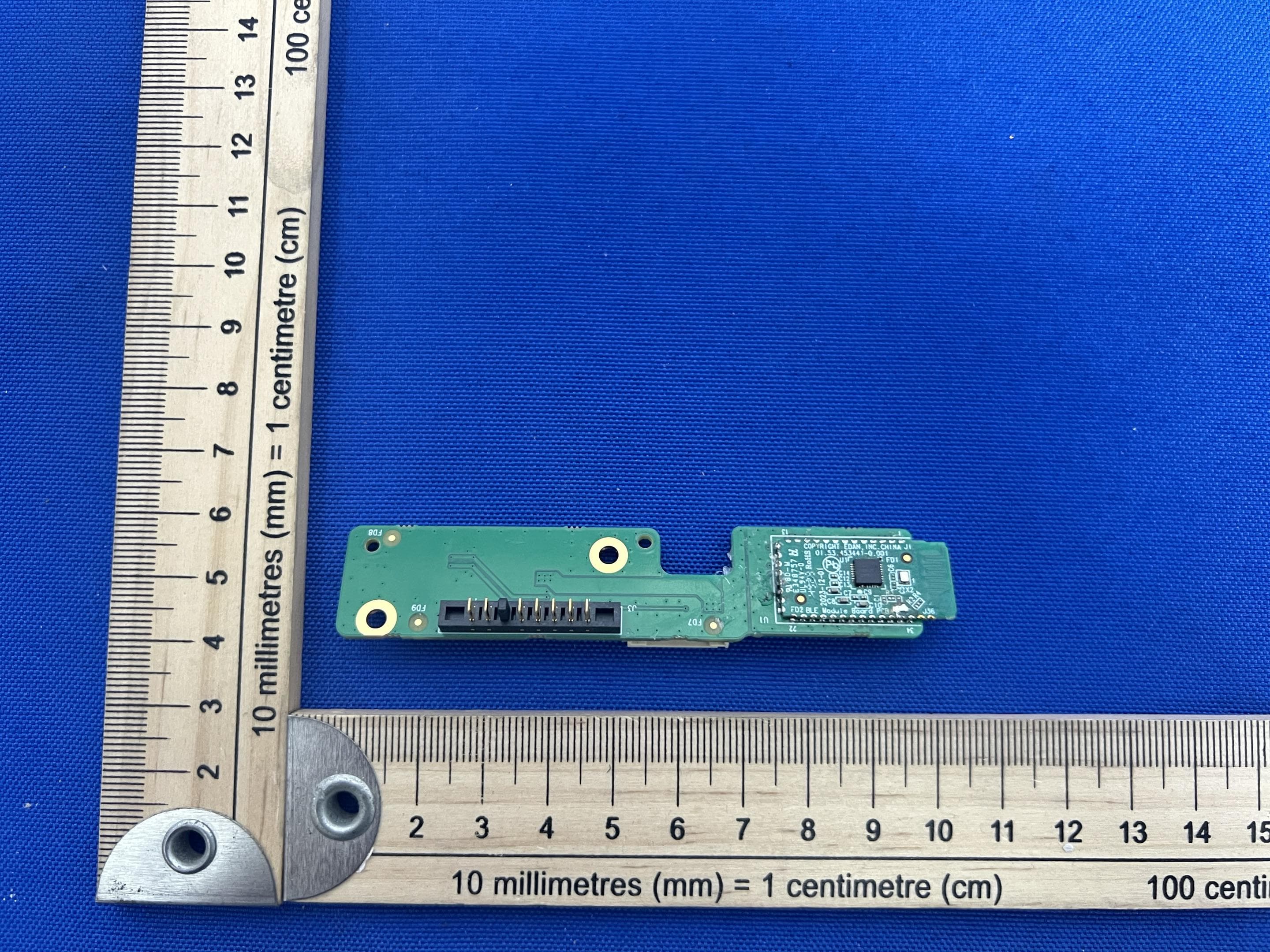
SMQIM3
May 06, 2026Bluetooth module
Equipment Class
DTS - Digital Transmission System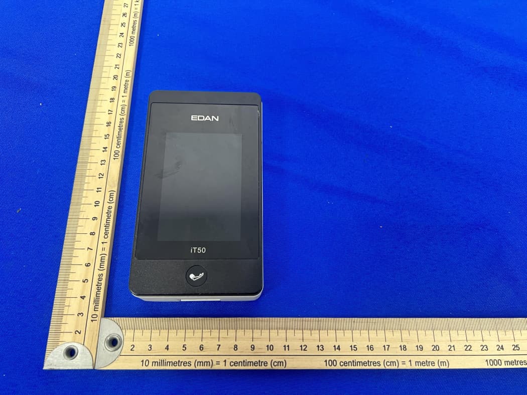
SMQIT50
Jan 30, 2026Telemetry Monitor
Equipment Class
DXX - Part 15 Low Power Communication Device TransmitterSMQIT30
Jan 28, 2026Shenzhen CTL Testing Technology Co., Ltd.
Equipment Class
NII - Unlicensed National Information Infrastructure TX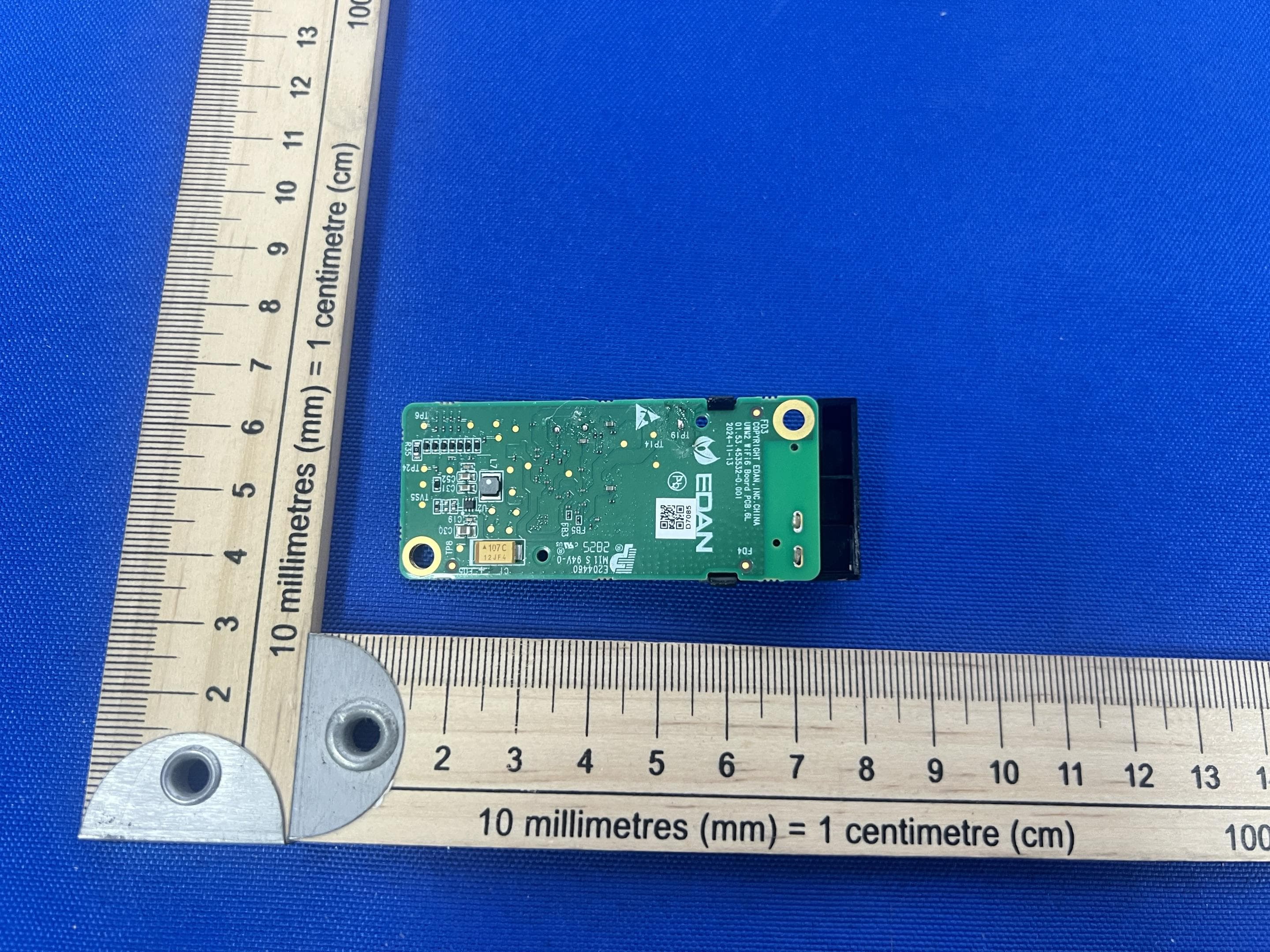
SMQUWM2
Dec 02, 2025WIFI module
Equipment Class
DTS - Digital Transmission System
SMQ-NANOC5
Sep 15, 2024Nano Series Diagnostic Ultrasound Systen
Equipment Class
NII - Unlicensed National Information Infrastructure TX