T4K-QZQX929Two Way Radio
Qixiang Electron Science& Technology Co., Ltd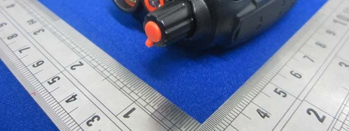
Click to zoom
Application Details
- Equipment Class
- TNF - Licensed Non-Broadcast Transmitter Held to Face
- Date of Grant
- Sep 10, 2013
- Application Purpose
- Original Equipment
- Date of Application
- Sep 10, 2013
- Equipment Note
- Two Way Radio
- Frequency Range
- 406.10000000 - 470.00000000
- Country
- China
Documents & Files
Document Text
Text extracted from the exhibit documents filed with the FCC. Open a document above to read the original.
Users Manual
for "Occupation Use Only" In addition, our radio complies with the following is designed for and classifed as "Occupation Use Only" meaning it must be used Safety training Information Our radio generates RF electromagnetic energy during transmit mode. This radio only during the course of employment by individuals aware of the hazards, and the ways to minimize such hazards. This radio is NOT intended for use by the "General Population"in an uncontrolled environment. This radio has been tested and complies with the FCC RF exposure limits Standards and Guidelines with regard to RF energy and electromagnetic energy levels and evaluation of such levels for exposure to humans: 1. FCC OET Bulletin 65 Edition 97-01 Supplement C, Evaluating Compliance with FCC Guidelines for Human Exposure to Radio Frequency Electromagnetic Fields. 2. American National Standards Institute (C95.1-1992), IEEE Standard for Safety Levels with Respect to Human Exposure to Radio Frequency Electromagnetic Fields, 3 kHz to 300 GHz. 3. American National Standards Institute (C95.3-1992), IEEE Recommended Practice for the Measurement of Potentially Hazardous Electromagnetic Fields- RF and Microwave. 4. The following accessories are authorized for use with this product. Use of accessories other than those (listed in the instruction) specified may result in RF exposure levels exceed the FCC requirements for wireless RF exposure. This device complies wit h part 15 of the FCC Rules. Operation is subject to the following two conditions: (1) This device may not cause harmful interference, and (2) this device must acceptany interference received, including interference that may cause undesired operation. Any Changes or modifications not expressly approved by the party responsible for compliance could void the user’s authority FCC Warning: to operate the equipment. when transmitting and only use our radio’s belt-clip which is listed in To ensure that your expose to RF electromagnetic energy is within the FCC allowable limits foroccupational use, always adhere to the following guidelines: 1. DO NOT operate the radio without a proper antenna attached, as this may damaged the radio and may also cause you to exceed FCC RF exposure limits. A proper antenna is the antenna supplied with this radio by the manufacturer or antenna specifically authorized by the manufacturer for use with this radio. 2. DO NOT transmits for more than 50% of total radio use time (“50% duty cycle”). Transmitting more than 50% of the time can cause FCC RF exposure compliance requirements to be exceeded. The radio is transmitting when the “TX indicator”lights red. You can cause the radio to transmit by pressing the “PTT”switch. 3. ALWAYS keep the antenna at least 2.5 cm (1 inch) away from the body instructions when attaching the radio to your belt, etc., to ensure FCC RF exposure compliance requirements are not exceeded. To provide the recipients of your transmission the best sound quality, hold the antenna at least 5 cm (2 inches) from your mouth, and slightly off to one side. The information listed above provides the user with the information needed to make him or her aware of RF exposure, and what to do to as*sure that this radio operates with the FCC RF exposure limits of this radio. Electromagnetic Interference/Compatibility During transmissions,our radio generates RF energy that can possibly cause interference with other devices or systems. To avoid such interference, turn off the radio in areas where signs are posted to do so. DO NOT operate the transmitter in areas that are sensitive to electromagnetic radiation such as hospitals, aircraft, and blasting sites. Occupational/Controlled Use The radio transmitter is used in situations in which persons are exposed as consequence of their employment provided those persons are fully aware of the potential for exposure and can exercise control over their exposure. THANK YOU! Thank you very much for choosing our transceiver. The transceiver provides you with reliable, clear and efficient communication service. Our 929 introduces innovative DSP (Digital Signal Processing) baseband technique to achieve high-fidelity voice processing and encryption. 929 is a compact and fashionable transceiver that allows you to enjoy instant communication at ease. The features like novelty, nice timbre, high power (4W), make 929 a high cost-effective professional transceiver. It is of unique and innovative functions, such as, oscillation and chord rings prompt missed calls, voice prompt battery capacity, jacklight and optional high-fidelity earphones fitted for using in Hotels, Amusement buildings, Emporium, Super shopping center, Estate management and other trades. Apart from these, the radio has long-distance anti-theft alarming, which makes it a good option for simple alarm device in vehicles. SAFETY INFORMATION FOR USER Our transceiver is excellently designed with advanced technology. Please observe the following precautions to perform your obligation, prevent personal injury and ensure the safety of transceiver usage. 1. Keep the transceiver and accessories away from children. 2. Please do not try to open or modify the transceiver without permission, non-professionals process may also cause damage. 3. Please use assorted battery and charger to avoid damage. 4. Please use assorted antenna to ensure the communication distance. 5. Please do not expose the transceiver to long period of direct sunlight, nor place it close to heat appliances. 6. Please do not put the transceiver in excessively dusty or humid areas. 7. Do not use harsh chemicals, cleaning solvents to clean the transceiver. 8. Do not transmit without antenna. 9. When using this transceiver, we recommend transmitting for 1 minute then receiving for 4 minutes. Continuous transmitting for long time or working in high power will heat the back of the transceiver. Do not place the transceiver’s hot back close to any surface of plastic. 10.If any abnormal odor or smoke detecte…
Text truncated - open the document above for the full version.
Block Diagram
929 LP F ANT SW D2 04 ,D2 12 HVC1 31 X2 Q2 05 2SK30 78 U2 00 RF MODULE ANT SW +3 .3V AUDIO AM P U2 05 BL 629 0 +5 V ANT VOLUME +5 V Q2 02 RQA0 009 FINAL AM PDR IVE AMP RD A1 846 Q2 10 2SC33 56 RF AM P 3T3 MIC 13 .00 0MHz X2 00 TX CO P2 4 (L NA, MIX , IF, RSSI, SQ, AFC, C TC SS/D CS, FM MOD EM, VCO, LOOP FIL TER , VOX) +3 .3V +5 V 5V REG. U2 01 BM 11 17 CX CH AR GE U2 07 KIA78 L09 D2 10 PR OTECTOR BATT 3.7V BATT POWER SW W200 B W200 A BATT1 U2 02 MUSIC-LY58 -M P3 2 P0 2P0 3 S Q P0 1, P 15 , P1 6, P 17 P2 1, P 22 V O X D E T D C S D E T RF IN RF OUT P1 2 MUSIC Au dio A U D I O T O N E P4 4, P 45 D2 06 RED(TX) D2 01 GR EEN(R X) S2 03 UP S2 04 DN P 2 6 P 2 7 P 0 4 P 0 5 U2 04 STC12 LE5 A3 2AD M ICR OPR OC ESSOR A - + 3V MOTO (10 30 -30) MG20 0 P4 3 Q2 07 DTC 14 3ZE BATT1 SW M OTOR SERVO RX D P0 4 P0 5 PTT FP 1 FP 2 P0 2 P1 0 P0 0P0 4 P0 5 P1 1 P0 3 D2 08 WHITE-LED SW P4 2 R2 07 DTC 11 4EE BATT1 P2 5 LS200 J 2 0 4 K E Y I N T E R F A C E J2 03 DC INTER FAC E P2 4 P2 3 P1 4 P1 1 I N T P1 2 40 0~4 70 MH z P1 2 T O N E . . U2 06 BATT AP C 3T3 SW SW SW P1 4/P A NJ M2 904 Q2 03 Q2 06 Q2 01 DTC 11 4EE DTC 14 4EE DTA 14 4EE SP EX T M IC M IC EX T SP MIC P0 0 RX D OP T D ET +3 .3V TX D +3 .3V Q2 04 ,Q2 11 DTA1 14EE DTC1 14EE +3 .3V Q2 12 ,Q2 13 DTC1 14EE P2 4 D2 02 ,D2 03 HSC2 77 X 2 EX T D C P2 3 P0 6 Emergency 3T3 3.3V REG . U2 08 ME62 06- 33M OSC 1 3.0 MH z O S C 1 3 . 0 M H z SW Q2 14 DTA 12 3JE +3 .3V 1N41 48 P2 5 P4 3 P4 2 P4 0 P3 6 P3 7 P3 2 RX D UTX 40 0~4 70 MH z M K20 0 J2 02 J2 01 +3 .3V +3 .3V PA EMER GENCY S1S2 FP 2 S3 FP 1 S4 PTT OSC AMP +3 .3V Q2 00 2SC46 17 11 4EE FQC P0 6 P0 7 S2 02 M ENU P 2 0 RF IN Q2 16 2SC44 26 RF AMP 3R 3 3R3 SW Q2 15 DTA 11 4EE GP IO3 GP IO3 BLOCK DIAGRAM
Cover Letter(s)
Federal Communications CommissionDA 13-431 Before the Federal Communications Commission Washington, D.C. 20554 In the Matter of Implementation of Sections 309(j) and 337 of the Communications Act of 1934 as Amended Promotion of Spectrum Efficient Technologies on Certain Part 90 Frequencies ) ) ) ) ) ) ) WT Docket No. 99-87 RM-9332 ORDER Adopted: March 15, 2013Released: March 18, 2013 By the Chief, Wireless Telecommunications Bureau, Chief, Public Safety and Homeland Security Bureau, and Chief, Office of Engineering and Technology: 1.Introduction.In this Order, we grant in part and deny in part a Petition to Delay Indefinitely Implementation of Section 90.203(j)(5) of the Commission’s Rules filed by Ritron, Inc. (Ritron) on September 21, 2012. 1 Pursuant to Section 90.203(j)(5) of the Commission’s rules, the Commission no longer accepts applications for certification of Part 90 private land mobile radio (PLMR) equipment in the 150-174 MHz and 450-512 MHz bands that cannot operate in a 6.25 kHz mode or with equivalent efficiency. 2 Ritron requests that implementation of this requirement be delayed indefinitely. We conclude that the requirement should be waived only until January 1, 2015. 2.Background.In 1995, the Commission adopted rule changes to promote the efficient use of the PLMR service and facilitate the introduction of advanced technologies. 3 To promote the transition to a more efficient narrowband channel plan, the Commission provided, inter alia, that “only increasingly efficient equipment” would be approved. 4 The Commissiondid not set a date after which it would no longer approve equipment with a wideband (25 kHz) mode, or after which such equipment could no longer be manufactured or used. 5 The Commission contemplated that, as systems reached the end of their service life and new radios were needed, users would migrate to the narrower bandwidth multi-mode radios in order to avoid the adjacent-channel interference that could occur from systems using the adjacent narrowband channels. 6 3.Subsequently, the Commission determined that the 1995 rules failed to provide adequate incentive to realize the Commission’s spectrum efficiency goals in these bands, and stronger measures 1 SeePetition to Delay Indefinitely Implementation Section 90.203(j)(5) of the Commission’s Rules (filed Sept. 21, 2012) (Petition). 2 See47 C.F.R. § 90.203(j)(5). 3 SeeReplacement of Part 90 by Part 88 to Revise the Private Land Mobile Radio Services and Modify the Policies Governing Them, Report and Order and Further Notice of Proposed Rule Making, PR Docket No. 92-235, 10 FCC Rcd 10076, 10077 ¶ 1 (1995). 4 Id.at 10081 ¶ 7. 5 Id.at 10100 ¶ 40. 6 Id. Federal Communications CommissionDA 13-431 2 would be required to bring about a timely transition to narrowband technology. 7 The Commission therefore amended the rules to provide that, by January 1, 2013, Industrial/Business and Public Safety Radio Pool licensees in the 150-174 MHz and 421-512 MHz bands must migrate to 12.5 kHz channel bandwidth or utilize a technology that achieves equivalent efficiency. 8 4.The Commission also adopted interim deadlines to facilitate this transition to narrowband technology. Among other rules, the Commission provided that, beginning January 1, 2011, it would no longer accept applications for certification of equipment that cannot operate in 6.25 kHz mode or with equivalent efficiency. 9 In 2010, the Commission temporarily waived this requirement until January 1, 2013, 10 but stated, “If 6.25 kHz standards still are not in place at that date, interested parties may request a further extension.” 11 5.Ritron, a manufacturer of wireless products, contends that standards for 6.25 kHz technology are not yet in place and that other issues exist that justify delaying implementation of mandatory 6.25 kHz certification by manufacturers.Ritron states that no one 6.25 kHz equipment standard exists and that, in the Industrial/Business sector of the market, two incompatible and proprietary technologies have emerged. 12 Italso argues that 6.25 kHz equipment is still unduly expensive. 13 Finally, Ritron asserts that using the equipment authorization process to facilitate the transition to narrowband technology has been largely unsuccessful. 14 Itconcludes that the implementation of Section 90.203(j)(5) should be delayed until (a) a real need has been established for additional PLMR frequencies beyond those created by the transition to 12.5 kHz channels; (b) the benefits of 6.25 kHz outweigh the associated research and development, manufacturing, and product costs; and (c) a standard has emergedfor a more cost-effective voice compressor/decompressor (vocoder). 15 6.The Wireless Telecommunications Bureau, Public Safety and Homeland Security Bureau and the Office of Engineering and Technology sought comment on Ritron’s request. 16 We asked commenters to address whether the public interest would be served by further delaying implementation of 7 See Implementation of Sections 309(j) and 337 of the Communications Act of 1934 as Amended,Second Report and Order and Second Further Notice of Proposed Rulemaking, WT Docket No. 99-87, 18 FCC Rcd 3034, 3038 ¶ 12 (2003). 8 See 47 C.F.R. § 90.209(b)(5). The January 1, 2013 deadline for converting to 12.5 kHz technology has been waived for licensees in the 470-512 MHz segment of the UHF band (the T-Band). SeeImplementation of Sections 309(j) and 337 of the Communications Act of 1934 as Amended, Order, WT Docket No. 99-87, 27 FCC Rcd 4213 (T-Band Order), on recon., Order on Reconsideration, 27 FCC Rcd 14770 (WTB/PSHSB/OET 2012). 9 See Implementation of Sections 309(j) and 337 of the Communications Act of 1934 as Amended,Third Report and Order, WT Docket No. 99-87, 22 FCC Rcd 6083, 6090 ¶ 16 (2007) (Third Report and Order). 10 See Implementation of Sections 309(j) and 337 of the Communications Act of 1934 as Amended, Order, WT Docket No. 99-87, 25 FCC Rcd 8861, 8866 ¶ 11 (2010) (Order). 11 Id.at 8866 n.41. 12 …
Text truncated - open the document above for the full version.
External Photos
EXHIBIT B - EUT EXTERNAL PHOTOGRAPHS EUT – Top View EUT – Bottom View EUT – Side View EUT – Side View EUT – Port View EUT – Earphone View EUT –Base Top View EUT –Base Bottom View EUT –Adapter View EUT – Adapter Label View
ID Label/Location Info
EXHIBIT A - FCC ID LABELING AND LOCATION FCC ID Label FCC ID Label Location The label shown shall be permanently affixed at a conspicuous location on the device and be readily visible to the user at the time purchase (Labeling requirements per 2.925) Label here
Internal Photos
EXHIBIT C - EUT INTERNAL PHOTOGRAPHS EUT – Battery Cover off View EUT –Uncover View EUT – Main Board Top View EUT – Main Board Bottom View EUT – Antenna View EUT –Base Uncover View EUT –Base Main Board Top View EUT –Base Main Board Bottom View
Operational Description
929 1 P 2 1 , P 2 2 AF SP MUTE P24 VOL D C S D E T U204 CPU P 0 3 S Q SW SP AF PA LS 200 J202 U205 Q212,Q213 P 3 2 U101 COMPANDER RF MODULE U200 ANT SW R F M O D U L E ANT AF AMP SP MIC RX/TX:400 ~ 470MHz FI NAL PRE DRI VE DRI VE R F AMP ANT SW RF MODULE ANT U200 D204,D212 D202,D203 Q200 OSC AMP TCXO 13.00MHz X200 13.00MHz SP AF PA AMP U205 AF VOL RF AMP Q216 43 MIC TCXO U204 CPU P13 RF MODULE U200 X200 CIRCUIT DESCRIPTION 1. Overview This transceiver is aUHF portable transceiver designed to operate in the frequency range of400to470MHz. The unit consists ofRFmodule, transmitter, power supply,APCcircuit,Compandercircuitand control circuits. 2.Frequency Configuration The frequency configuration is shown in Figure 1 and Table 1. Fig. 1 Frequency configuration 3.Receiver System 3-1.ReceiverCircuit The received signal from the antenna passes through a low-passfilter and then through a transmission/reception switching circuit (antenna switch)and isdemodulatedby theRF module U200 (LNA, MIX,IF,RSSI,CTCSS/DCS, VCO,AFC,MOD,PLL,LOOP FILTER,VOX,DTMFand PRE/DE-EMPHASIS).The demodulated signal is routed to the audio circuit.(See Fig.2) Fig.2 3-2.Audio Amplifier Circuit TheAudiosignal fromU200goes toAF amplifier(U205). The signal then goes through an AF volume control , and is routed to an audio power amplifier (U205) where it is amplified and output to the speaker.(See Fig.3) 3-3.Squelch And the noise component is amplified and rectifiedby a filter and an amplifier to produce a DC voltage corresponding to the noise level. The DC signal from the RF module goes to the analog port of themicroprocessor (U204). U204 determines whether to output sounds from the speaker by checking whether the input voltage is higher or lower than the preset value. To output sounds from the speaker, U204 sends a high signal to the P24 line and turns U205 on through Q212, Q213 and U205. (See Fig.3) Fig.3 3-3.CTCSS/DCS The output signal fromRF module(U200) enters the microprocessor(U204).U204determineswhether the CTCSSor DCSmatches the preset value, andcontrols the P24and the speaker outputsoundsaccording to the squelch results.(See Fig.3) 4. Transmission signal system 4-1.Microphone Amplifier Circuit The signal from the microphone goes to the RFmodule (U200)modulation.(See Fig.4) 4-2. CTCSS/DCS CTCSS/DCS signal transmit through RF module(U200) inter generator,mixes with the audio signal, then input into inter modem.(See Fig.4) Fig.4 929 2 BA TT1 R237 C271 P1 0 R271 40 U204 CPU ANT LPF U206A ANT SW FI NAL AMP RF DRIVE AMP RF AMP Fr om RF module (U200 ) +BATT (2/2 ) U206B (1 /2) R251 R249 R246 APC (U204 ) VDDVGVG Q210Q205Q20 2D20 4,D212 POWER BATT1 ON/OFF 3.3V 3.3V REG. U208 P25 BATT 5V 5V REG. U201 RF power amp (Q202) 3T3 Q214 DC SW GPIO3 3R3 Q215 DC SW CIRCUIT DESCRIPTION 4-3.Drive and Final AmplifierCircuit The signal from theRFmodule(U200) is amplified by the pre-drive (Q210) and drive amplifier (Q205) to40mW. The output of the drive amplifier is amplified by the RF power amplifier (Q202) to4W (1W when the power is low). The RF power amplifier consists of two MOS FET stages. The output of the RF power amplifieris then passed through the harmonic filter (LPF) and antenna switch (D204and D212) and applied to the antenna terminal.(See Fig.5) Fig.5 4-4.APCCircuit The APC circuit always monitors the current flowing through the RF power amplifier (Q202)and keeps a constant current. The voltage drop atR246, R249and R251is caused by the current flowing through the RF power amplifier and this voltage is applied to the differential amplifierU206B(2/2).U206A(1/2) compares the output voltage ofU206(2/2) with the reference voltage fromU204. The output ofU206A(1/2) controls the VG of the RF power amplifier, Drive amplifier and Pre-Drive amplifier to make both voltages the same. The change of power high/low is carried out by the change of the referencevoltage.(See Fig.5) 5Control Circuit The microprocessor (U204)operates at a clock of 13.000MHz. The control circuit consists of a microprocessor (U204) and its peripheral circuits. It controls the TX-RX unit. U204 mainly performs the following: (1)Switching between transmission and reception by the PTT signal input. (2) Reading system,tone, frequency, and program data from the memory circuit. (3) Controlling squelch on/off by the DC voltage from the squelch circuit. (4)Controlling the audio mutecircuitby the decode data input. (5) Transmitting tone and encode data 5-1. Low battery warning The battery voltage is monitored by the microprocessor (U204). When the batteryvoltage falls below the voltage set by the Low BatteryWarning adjustment, the red LED flashes to notify the operator that it is time to replace the battery. If the battery voltage falls even more (approx. 6.0V), a beep sounds and transmission is stopped.(See Fig.6) Low battery warningBattery condition The red LED flashes during transmission The battery voltage is low but the transceiver is still usable. The red LED flashes and a continuous beep soundswhilePTT pressed. The battery voltage is low and the transceiver is not usable to make calls. Fig.6 6.Power Supply Battery +B is supplied via aferrite chipfrom the battery terminalconnected to the TX-RX unit. After passing through the powerswitch, power supply (BATT1) is applied to the three AVRs.U201supplies 5V (5V) to the common circuits, andU206supplies3.3V(3.3V) to common circuits. Duringtransmission,P25becomes Low and Q211is turned ON tosupply3T3(3.3V) to the TX circuit. Duringreception,GPIO3becomes Low and Q213is turned ON tosupply3R3(3.3V) to theRX circuit. (See Fig.7) Fig.7
Parts List/Tune Up Info
Common Section Test equipment TerminalMethod 1. Setting 1) BATT terminal voltage: 7.4V 2) SSG standard modulation Transmitter section Test equipment TerminalMethod 1. Transmit frequency TEST CH: center PTT: ON Frequency count e1. Connect the antenna connector of EUT with the Frequency counter. 2. Open the Tuner software, go to frequency adjust item, 3. Observe the frequency displayed on Freqeuncy counter, and adjust the vernier until the frequency offset is less than or equals to 100 Hz. 4. Click the “Write” button to save your settings. Within ±100Hz 2. High power Adjust TEST CH: low, center, high Battery terminal: 7.4V PTT: ON 4.0W ±0.5W 1.45 A or less 3. Low power Adjust CH: low, center, high Battery terminal: 7.4V PTT: ON 1.0W ±0.3W 0.8 A or less 4. MAX DEV Adjust TEST CH: Center PTT: ON Power meter Deviation meter Oscilloscope AG AF VTVM ANT SP/MIC connector 1. Connect EUT to test equpiment . 2. Open the Tuner software, go to Deviation item. 4. Observe the frequency deviation , and adjust the vernier until it is 2.1k± 100Hz. 6. Click the “Wirte” button to save your settings. 2.1 kHz ±100Hz Power meter Ammeter ANT 1. Connect the antenna connector of EUT with the Power meter and contenct a ammeter. 2. Open the Tuner software, go to High/Low TX power adjust items, 3. Observe the frequency displayed on Freqeuncy counter, and adjust the vernier until the output power is 4.0W ±0.5W 1.45 A or less(high) 1.0W ±0.3W 0.8 A or less(low) 4. Click the “Write” button to save your settings. Specifications /Remarks ItemCondition Measurement Specifications /Remarks ItemCondition Measurement 929 1 PARTS LIST Ref. NoParts No.Description of itemSize(LxW)(mm)QtySpecification C100SMT CAPACITOR04021102±10% 50V C101SMT CAPACITOR0402115P±5% 50V C102SMT CAPACITOR04021103±10% 50V C103SMT CAPACITOR04021NO USE C104SMT CAPACITOR06031105±10% 50V C105SMT CAPACITOR04021NO USE C106SMT CAPACITOR04021104±10% 50V C107-C109SMT CAPACITOR04023NO USE C110SMT CAPACITOR04021NO USE C111SMT CAPACITOR04021NO USE C112SMT CAPACITOR04021NO USE C200SMT CAPACITOR04021100P±5% 50V C201-C202SMT CAPACITOR04022103±10% 50V C203-C204SMT CAPACITOR04022470P±10% 50V C205SMT CAPACITOR04021102±10% 50V C206SMT CAPACITOR0402110P±5% 50V C207-C208SMT CAPACITOR04022103±10% 50V C209SMT CAPACITOR06031NOUSE C210SMT CAPACITOR04021470P±10% 50V C211SMT CAPACITOR04021102±10% 50V C212SMT CAPACITOR04021103±10% 50V C213SMT CAPACITOR04021102±10% 50V C214-C215SMT CAPACITOR04022103±10% 50V C216SMT CAPACITOR04021104±10% 50V C217SMT CAPACITOR06031103±10% 50V C218SMT CAPACITOR06031105±10% 50V C219SMT CAPACITOR04021103±10% 50V C220-C222SMT CAPACITOR04023104±10% 50V 929 2 PARTS LIST Ref. NoParts No.Description of itemSize(LxW)(mm)QtySpecification C223SMT CAPACITOR04021103±10% 50V C224SMT CAPACITOR04021220P±5% 50V C225SMT CAPACITOR04021103±10% 50V C226SMT CAPACITOR04021104±10% 50V C227SMT CAPACITOR04021102±10% 50V C228-C229SMT CAPACITOR04022103±10% 50V C230-C231SMT CAPACITOR04022100P±5% 50V C232SMT CAPACITOR04021104±10% 50V C233SMT CAPACITOR04021NO USE C234SMT CAPACITOR04021103±10% 50V C235SMT CAPACITOR04021104±10% 50V C236SMT CAPACITOR04021103±10% 50V C237SMT CAPACITOR04021473±10% 50V C238SMT CAPACITOR04021103±10% 50V C239SMT CAPACITOR04021102±10% 50V C240SMT CAPACITOR04021103±10% 50V C241SMT CAPACITOR04021102±10% 50V C242SMT CAPACITOR04021104±10% 50V C243SMT CAPACITOR06031105±10% 50V C244SMT CAPACITOR04021104±10% 50V C245SMT CAPACITOR04021103±10% 50V C246SMT CAPACITOR06031105±10% 50V C247SMT CAPACITOR04021NO USE C248-C249SMT CAPACITOR08052225±10% 50V C250SMT CAPACITOR04021102±10% 50V C251SMT CAPACITOR04021100P±5% 50V C252SMT CAPACITOR08051225±10% 50V C253SMT CAPACITOR06031100P±5% 50V 929 3 PARTS LIST Ref. NoParts No.Description of itemSize(LxW)(mm)QtySpecification C254SMT CAPACITOR04021103±10% 50V C255SMT CAPACITOR04021102±10% 50V C256SMT CAPACITOR04021103±10% 50V C257-C258SMT CAPACITOR04022273±10% 50V C259SMT CAPACITOR04021103±10% 50V C260SMT CAPACITOR08051225±10% 50V C261-C262SMT CAPACITOR04022103±10% 50V C263-C264SMT CAPACITOR04022103±10% 50V C265SMT CAPACITOR06031103±10% 50V C266SMT CAPACITOR04021103±10% 50V C267C-C269SMT CAPACITOR04022102±10% 50V C270SMT CAPACITOR040211.5P±0.1P50V C271SMT CAPACITOR04021104±10% 50V C272SMT CAPACITOR0402122P±5% 50V C273SMT CAPACITOR04021470P±10% 50V C274SMT CAPACITOR04021103±10% 50V C275SMT CAPACITOR04021470P±10% 50V C276SMT CAPACITOR06031470P±10% 50V C277SMT CAPACITOR06031105±10% 50V C278SMT CAPACITOR06031470P±10% 50V C279SMT CAPACITOR04021103±10% 50V C280SMT CAPACITOR0402112P±5% 50V C281SMT CAPACITOR04021103±10% 50V C282SMT CAPACITOR04021470P±10% 50V C283-C284SMT CAPACITOR04022102±10% 50V C285SMT CAPACITOR04021104±10% 50V C286SMT CAPACITOR0402122P±5% 50V C287SMT CAPACITOR04021NO USE 929 4 PARTS LIST Ref. NoParts No.Description of itemSize(LxW)(mm)QtySpecification C288SMT CAPACITOR06031105±10% 50V C289-C290SMT CAPACITOR04022NO USE C291SMT CAPACITOR04021104±10% 50V C292SMT CAPACITOR0402110P±0.25P50V C293SMT CAPACITOR0603156P±5% 50V C294SMT CAPACITOR060314P±0.1P50V C295SMT CAPACITOR060315P±0.1P50V C296-C297SMT CAPACITOR060323P±0.1P50V C298-C301SMT CAPACITOR06033NO USE C302SMT CAPACITOR04021NO USE C303SMT CAPACITOR06031564±10% 50V C304SMT CAPACITOR0603111P±5% 50V C305SMT CAPACITOR04021223±10% 50V C306SMT CAPACITOR0603124P±5% 50V C307SMT CAPACITOR060318P±0.25P50V C308SMT CAPACITOR060319P±0.25P50V C309SMT CAPACITOR060314P±0.1P50V C310SMT CAPACITOR04021120P±5% 50V C311SMT CAPACITOR04021104±10% 50V C312SMT CAPACITOR04021102±10% 50V C313SMT CAPACITOR04021104±10% 50V C314SMT CAPACITOR04021470P±10% 50V C315SMTCAPACITOR04021102±10% 50V C316SMT CAPACITOR04021NO USE C317SMT CAPACITOR040215P±0.1P50V C318SMT CAPACITOR04021NO USE C319SMT CAPACITOR04021470P±10% 50V C320SMT CAPACITOR04021NO USE 929 5 PARTS LIST Ref. NoParts No.Description of itemSize(LxW)(mm)QtySpecification C321SMT CAPACITOR04021470P±10% 50V C322SMT CAPACITOR04021150P±5% 50V C323SMT CAPACITOR04021103±10% 50V C324-C325SMT CAPACITOR06032105±10% 50V C326-C331SMT CAPACITOR04026103±1…
Text truncated - open the document above for the full version.
RF Exposure Info
Note: This test report is prepared for the customer shown above and for the device described herein. It may not be duplicated or used in part without prior written consent from Bay Area Compliance Laboratories Corp. SAR EVALUATION REPORT For Qixiang Electron Science & Technology Co., Ltd. Qixiang Building, Tangxi Industrial Zone, Luojiang District, QuanZhou 362011, Fujian Province, China FCC ID: T4K-QZQX929 Report Type: Original Report Product Type: Two Way Radio Test Engineer: Sandy Wang Report Number: R1XM130513002-20 Report Date: 2013-08-08 Reviewed By: Alvin Huang RF Leader Prepared By: Bay Area Compliance Laboratories Corp. (Shenzhen) 6/F, the 3rd Phase of WanLi Industrial Building ShiHua Road, FuTian Free Trade Zone Shenzhen, Guangdong, China Tel: +86-755-33320018 Fax: +86-755-33320008 www.baclcorp.com.cn Bay Area Compliance Laboratories Corp. (Shenzhen) Report No: R1XM130513002-20 SAR Evaluation Report 2 of 62 Attestation of Test Results Company Name Qixiang Electron Science & Technology Co., Ltd. EUT Description Two Way Radio FCC ID T4K-QZQX929 Model Number 929/909/919/929G/938G/959/999 EUT Information Test Date 2013-08-02 Mode Frequency (MHz) Max. SAR Level(s) Report Limit (W/Kg) Analog 400-470 12.5kHz Face up: 1.055 W/kg (50% duty cycle) Body-Back: 5.717 W/kg (50% duty cycle) 8 ANSI / IEEE C95.1: 2005 IEEE Standard for Safety Levels with Respect to Human Exposure to Radio Frequency Electromagnetic Fileds,3 kHz to 300 GHz. ANSI / IEEE C95.3: 2002 IEEE Recommended Practice for Measurements and Computations of Radio Frequency Electromagnetic Fields With Respect to Human Exposure to SuchFields,100 kHz—300 GHz. IEEE1528:2003 IEEE Recommended Practice for Determining the Peak Spatial-Average Specific Absorption Rate (SAR) in the Human Head from Wireless Communications Devices: Measurement Techniques Applicable Standards PART 2.1093 Radiofrequency radiation exposure evaluation: portable devices Note: This wireless device has been shown to be capable of compliance for localized specific absorption rate (SAR) for General Population/Uncontrolled Exposure limits specified in ANSI/IEEE Standards and has been tested in accordance with the measurement procedures specified in IEEE 1528-2003 and RF exposure KDB procedures. The results and statements contained in this report pertain only to the device(s) evaluated. Bay Area Compliance Laboratories Corp. (Shenzhen) Report No: R1XM130513002-20 SAR Evaluation Report 3 of 62 TABLE OF CONTENTS DOCUMENT REVISION HISTORY .........................................................................................................................4 EUT DESCRIPTION ....................................................................................................................................................5 TECHNICAL SPECIFICATION.........................................................................................................................................5 REFERENCE, STANDARDS, AND GUILDELINES ...............................................................................................6 SAR LIMITS.................................................................................................................................................................7 FACILITIES AND ACCREDITATION .....................................................................................................................8 DESCRIPTION OF TEST SYSTEM ..........................................................................................................................9 EQUIPMENT LIST AND CALIBRATION .............................................................................................................16 EQUIPMENTS LIST & CALIBRATION INFORMATION....................................................................................................16 SAR MEASUREMENT SYSTEM VERIFICATION ............................................................................................…
Text truncated - open the document above for the full version.
Contact Information
Applicant
Ken Xu
Test Firm
Bay Area Compliance Laboratories Corp. (Dongguan)John Chan
[email protected]86-769-86858888
Technical Specifications
| # | Rule Parts | Frequency Range | Power Output | Emission | Tolerance |
|---|---|---|---|---|---|
| 2 | 9 | 406.1 MHz - 470 MHz | 4 W | 10K2F3E | 0.2 ppm |
Other Applications from Qixiang Electron Science& Technology Co., Ltd

T4K-AT5100
Jul 28, 202610 METER AMATEUR RADIO
Equipment Class
DTS - Digital Transmission System
T4K-UA1
Apr 07, 2026HANDHELD TRANSCEIVER
Equipment Class
CSR - Scanning Receiver
T4K-UVA1
Mar 30, 2026DUAL BAND HANDHELD TRANSCEIVER
Equipment Class
CSR - Scanning Receiver
T4K-AT-505
Jan 19, 2026CB Radio
Equipment Class
JAV - Other Non-Digital SDoC Devices
T4K-D890UV
Jan 07, 2026Multi-Protocol Digital+Analog Handheld Radio
Equipment Class
DSS - Part 15 Spread Spectrum Transmitter