T82HRF-2401Equipment built-in 2.4GHz band transceiver module
Herutu Electronics Corporation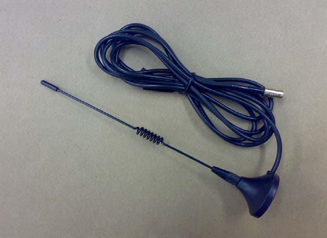
Click to zoom
Application Details
- Equipment Class
- DTS - Digital Transmission System
- Date of Grant
- Aug 25, 2015
- Application Purpose
- Original Equipment
- Date of Application
- Aug 25, 2015
- Equipment Note
- Equipment built-in 2.4GHz band transceiver module
- Frequency Range
- 2403.00000000 - 2478.00000000
- Country
- Japan
Documents & Files
Document Text
Text extracted from the exhibit documents filed with the FCC. Open a document above to read the original.
Users Manual
62-1 Toyooka-cho, Kita-ku, Hamamatsu-shi Shizuoka-ken, Japan 433-8103 TEL +81-53-438-3511 FAX +81-53-438-3411 : Product name Product type HRF-2401 ENG.DEPT Drawing Number Approved Checked 2015.08.03 : 2015.08.03 Drawn DC15002-02 Date Product Specification Issued sign Person 2015.08.03 FUJITA UEDA 2.4GHz band wireless module HERUTU ELECTRONICS CORPORATION 2015.08.03 ENG.DEPT SALES NAKAI ISSUED '15.08.03 HERUTU HERUTU ELECTRONICS CORPORATION 1.Summary ・HRF-2401 is 2.4GHz band wireless module. ・CPU is mounted in HRF-2401.It can be used by arranging only an input/output circuit to motherboard. ・HRF-2401 can work by coin battery or dry battery. ・It can be selected from 4 kinds of antennas by customer situation. ・HRF-2401 can not work by itself.It is necessary to be mounted to motherboard. IMPORTANT NOTE: i.That module is limited to OEM installation only. ii.That OEM integrators is responsible for ensuring that the end-user has no manual instructions to remove or install module. iii.That module is limited to installation in mobile or fixed applications, according to Part 2.1091(b) iv.That separate approval is required for all other operating configurations, Manual Information to the End User The OEM integrator has to be aware not to provide information to the end user regarding how to install or remove this RF module in the user’s manual of the end product which integrates this module. The end user manual shall include required regulatory information/warning as below. i.End-users must be provided with transmitter/antenna installation requirements and operating conditions for satisfying RF exposure compliance. ii.A separate section should clearly state “FCC RF Exposure requirements:” iii.Required operating conditions for end users iv.Antenna/or transmitter installation requirements. Labelling Requirements for the Host device The host device shall be properly labelled to identify the modules within the host device. The Industry Canada certification label of a module shall be clearly visible at all times when installed in the host device, otherwise the host device must be labelled to display the Industry Canada certification number of the module, preceded by the words “Contains transmitter module”, or the word “Contains”, or similar wording expressing the same meaning, as follows: Contains transmitter module IC: 10608A-HRF2401 where 10608A-HRF2401 is the module’s certification number. The applicant for equipment certification of the module shall provide with each unit of the module either a label such as described above, or an explanation and instructions to the user as to the host device labelling requirements. HRF-2401(2.4GHz band wireless module) Page 1/8 Subject Product Specification Document Name HERUTU ELECTRONICS CORPORATION 2.Specification ■General specification ■Wireless Specification *1 Antenna is used only 1 type from 4kinds Internal antenna ①1/4λ Dipole chip antenna External antenna ②1/4λ Dipole antenna(Flying Lead and U-FL connector) ③1/2λ Dipole antenna(SMB Male connector) ④1/2λ Dipole antenna(SMB Male connector) Magnet Base / Cable:RG174-1.5m Frequency 2403MHz~2478MHz 2/8 1MHz Half duplex Data rate 250kbps Frequency deviation Number of channel Channel spacing Mode of operation Product Specification HRF-2401(2.4GHz band wireless module) Soecification Transmit power 2.1mW Frequency error ±30ppm 2.05V~6.0V(Inside 2.0V) Power source 0°C~50°C/RH Under 85% Transmition approx 17.0mA/Receiving approx 18.5mA Standby Max 5.5μA Usage environment Current Consumption Quority of Material Shield case:C7521P t=0.15/basis material 20mm×32mm×3mm Specification nRF24LE1-F16Q48 Flash memory 16kByte/RAM 1kByte Product type F1D GFSK ±160kHz page 76ch 16MHz Emission desingnation Type of Modulation HRF-2401 Antenna type *1 Crystal oscillation frequency Document Name Subject Item External dimensions Item Device HERUTU ELECTRONICS CORPORATION ■Communication format ①Trnasmitting and receiving data format ※Customer can use this data area. ②Transmission interval → 1mS ←→ 1mS ← Data transmission time 1mS+Stop time approx 5mS ->1cycle(Approx 6mS) Customer data 13byte Check Sum 1byte Payload 21byte Address 5byte CRC 2byte Preamble 1byte Trnasmission time approx 1.0mS → ← Document Name Product Specification Command 1byte Sequence Number 1byte page 3/8 Subject HRF-2401(2.4GHz band wireless module) Approx5mS ID Number 5byte HERUTU ELECTRONICS CORPORATION ■Interface specification *2 *3 *4 *5 SpecificationItem Serial Communication Document Name Subject *In case of the chip antenna specification, the coaxial connector for external antennas is made non-mounting. Product Specification 4/8 Terminal shape GP-IO *3 Coaxial connector *2 ・Input/Output port number Maximum 30lines ・PWM 2CH(Frequency range:4khz~254kHz) ・ADC Resolusion performance Maximum 12bit For external antenna:20279-001E-01 ・UART Synchronous system:Asynchromous communication Communication speed:Under 38400bps Start bit :1bit Data length :8bit Stop bit :1bit Parity bit :none Flow sequence :none ・I2C Standard mode(100kbps) High speed mode(400kbps) ・SPI Slave(8Mbps) *4 page Side throw hole(1.5mm pitch) *5 Terminal number:35pin A serial communication shares a part port with an input/output port and PWM/ADC. It isn't possible to overlap and use. Communication speed for SPI port is limited depending on a resistance to be connected. Also there are 3 pin of side throw hole to fix the shield case. When it is mounted,a module has to fix to motherboard by solder for fixed reinforcement. HRF-2401(2.4GHz band wireless module) HERUTU ELECTRONICS CORPORATION 3.Operating explanation 4.Block diagram Selected only 1 antenna 16MHz HRF-2401 do a pairing with an equipment to communicate before wireless communicating. Piring way is different by a specification of included the interface electric substract. One is to match each ID by dipswitch,one is transmitter send ID data by registration switch,receiver register the ID data received from transmitter. There are several ways for re…
Text truncated - open the document above for the full version.
External Photos
1/2 ①1/4λ Dipole chip antenna ②1/4λ Dipole antenna (Flying Lead and U-FL connector) HERUTU ELECTRONICS CORPORATION 2/2 ③1/2λ Dipole antenna (SMB Male connector) ④1/2λ Dipole antenna (SMB Male connector) Magnet Base/Cable:RG174-1.5m ③④Connecting cable HERUTU ELECTRONICS CORPORATION
External Photos
Chip AntennaEXT Antenna
ID Label/Location Info
HRF-2401 Outline Drawing
Internal Photos
Chip AntennaEXT Antenna Chip AntennaEXT Antenna
RF Exposure Info
e-OHTAMA, LTD. Tokyo LaboratoryTest Report Number EOTEL133 2-8-20 Kurigi, Asao-ku Kawasaki-shi, Kanagawa, 215-0033 JapanForm Rev. 1.00 TEL: +81-44-980-2091 Page 2 of 2 1.Calculation According to 15.247(i) and 1.1307(b)(1),systems operating under the provisions of this section shall be operated in a manner that ensures that the public is not exposed to radio frequency energy level in excess of the Commission’s guidenlines. The 1-g and 10-g SAR test exclusion thresholds for 100MHz to 6GHz at test separation distances ≦50mm are determine by: [(max power of channel,including tune-up tolerance,mW])/(minimum test separation distance,mm)] [√f (GHz) ]≦3.0 for 1-g SAR and≦7.5 for 10-g extremity SAR ,Where ・f(GHz) is the RF channel transmit frequency in GHz. ・Power and distance are rounded to the nearest mW and mm before calculation. ・The result is rounded to one decimal place for comparison. The test exclusions are applicable only when the minimum test separation distance is≦50mm and for transmission frequencies between 100MHz and 6GHz.When the minimum test separation distance is <5mm,a distance of 5mm is applied to determine SAR test exclusion. Routine SAR evaluation refers to that specifically required by 2.1093, using measurements or computer simulation.When routine SAR evaluation is not required,portable transmitter with output power greater than the applicable low threshold require SAR evaluation to qualify for TCB approval. Result=P√F/D P:Maximum turn-up power in mW F:Channel Frequency in GHz D:Minumum test separation distance in mm 2.Results CH Frequency (MHz) Conducted Power (dBm) Tune Up Power (dBm) Max Tune Up Power (dBm) Max Tune Up Power (mW) ResultLimit L24031.321.0±12.01.5850.493 M24411.291.0±12.01.5850.503 H24781.071.0±12.01.5850.503 Table 1 RF Exposure Requirements Result:Pass
Test Report
e-OHTAMA, LTD. Tokyo LaboratoryTest Report Number EOTEL130 2-8-20 Kurigi, Asao-ku Kawasaki-shi, Kanagawa, 215-0033 JapanForm Rev. 1.00 TEL: +81-44-980-2091 Page 2 of 36 Page Cover Page.......................................................................................................................................................1 Table of Contents..............................................................................................................................................2 1.Summary ................................................................................................................................................ 3 1.1Terms and definitions .................................................................................................................... 3 1.2Standard(s) and Result.................................................................................................................. 4 1.3Test Methodology .......................................................................................................................... 4 2.Equipment Under Test (EUT) ................................................................................................................. 5 2.1General Descriptions ..................................................................................................................... 5 2.2Detailed Descriptions..................................................................................................................... 5 2.3Worst-Case Configuration and Mode ............................................................................................ 5 2.4Operation Mode(s) of the EUT for EMC during the Test(s) ........................................................... 5 2.5Peripheral Devices ........................................................................................................................ 5 2.6Interconnecting Cables .................................................................................................................. 6 2.7System Configuration .................................................................................................................... 6 2.8Labeling Requirements.................................................................................................................. 7 2.9Antenna Requirements .................................................................................................................. 7 2.10Modular transmitter Requirements ................................................................................................ 8 3.Test Data................................................................................................................................................ 9 3.1Test specification........................................................................................................................... 9 3.26dB Bandwidth ............................................................................................................................ 10 3.3Maximum Peak Output power ..................................................................................................... 13 3.4Band Edge of Compliance of RF Conducted Emmissions........................................................... 16 3.5Peak Power Spectral Density ...................................................................................................... 18 3.6Line Conducted Measurement..................................................................................................... 21 3.7Radiated emission ....................................................................................................................... 25 4.Test facility ........................................................................................................................................... 32 4.1Test Instruments.......................................................................................................................... 32 4.2Test equipment............................................................................................................................ 32 Annex A (Miscellaneous Information) ........................................................................................................... 33 A.1Test Locations ............................................................................................................................. 33 Annex B (Description of Test Method) .......................................................................................................... 34 B.1Conducted Emissions (AC Main and Other Terminals) ............................................................... 34 B.2Radiated Electric-Field Emissions (30 MHz to 1000MHz) ........................................................... 34 B.3Radiated Electric-Field Emissions above 1000MHz .................................................................... 35 B.4Radiated Magnetic-Field Emissions ............................................................................................ 36 e-OHTAMA, LTD. Tokyo LaboratoryTest Report Number EOTEL130 2-8-20 Kurigi, Asao-ku Kawasaki-shi, Kanagawa, 215-0033 JapanForm Rev. 1.00 TEL: +81-44-980-2091 Page 3 of 36 1. Summary 1.1 Terms and definitions AV Average DoC Declaration of Conformity EUT Equipment Under Test PK Peak QP Quasi-peak e-OHTAMA, LTD. Tokyo LaboratoryTest Report Number EOTEL130 2-8-20 Kurigi, Asao-ku Kawasaki-shi, Kanagawa, 215-0033 JapanForm Rev. 1.00 TEL: +81-44-980-2091 Page 4 of 36 1.2 Standard(s) and Result Applied Standard(s)Normative Reference(s)ClassificationResultNote FCC Part15 Subpart C6dB Bandwidth15.247(a)(2)Pass Maximum Peak Output Power15.247(b)(3)Pass Band Edge of Compliance of RF Conducted Emissions 15.247(d)Pass Peak Power Spectral Density15.247(e)Pass Line Conducted Measurement15.207Pass Radiated emissions15.209 15.205 Pass 1.3 Test Methodology All mesurements contained in t…
Text truncated - open the document above for the full version.
Test Setup Photos
e-OHTAMA, LTD. Tokyo Laboratory 2-8-20 Kurigi, Asao-ku Kawasaki-shi, Kanagawa, 215-0033 Japan TEL: +81-44-980-2091 Page 1 of 5 Test setup Photographs 1 EUT Photo1 1/4λDipole chip antenna Photo2 1/4λDipole antenna(Flying Lead and U-FL connector) e-OHTAMA, LTD. Tokyo Laboratory 2-8-20 Kurigi, Asao-ku Kawasaki-shi, Kanagawa, 215-0033 Japan TEL: +81-44-980-2091 Page 2 of 5 Photo3 1/2λDipole antenna(SMB Male connector) Photo4 1/2λDipole antenna(SMB Male connector) Magnet Base e-OHTAMA, LTD. Tokyo Laboratory 2-8-20 Kurigi, Asao-ku Kawasaki-shi, Kanagawa, 215-0033 Japan TEL: +81-44-980-2091 Page 3 of 5 2 Radiated Photo5 Test setup for radiated (9kHz-30MHz) Photo6 Test setup for radiated (30-300MHz) e-OHTAMA, LTD. Tokyo Laboratory 2-8-20 Kurigi, Asao-ku Kawasaki-shi, Kanagawa, 215-0033 Japan TEL: +81-44-980-2091 Page 4 of 5 Photo7 Test setup for radiated (300-1000MHz) Photo8 Test setup for radiated (above 1GHz) e-OHTAMA, LTD. Tokyo Laboratory 2-8-20 Kurigi, Asao-ku Kawasaki-shi, Kanagawa, 215-0033 Japan TEL: +81-44-980-2091 Page 5 of 5 3 Conducted Photo9Test setup for conducted(RF Test) Photo10Test setup for conducted(AC Line)
Contact Information
Applicant
Yoshiyasu Ueda
Test Firm
e-OHTAMA LTD., Tokyo EMC CenterHidekazu Taguchi
Technical Specifications
| # | Rule Parts | Frequency Range | Power Output |
|---|---|---|---|
| 1 | 15C | 2.40 GHz - 2.48 GHz | 1.36 mW |
Other Applications from Herutu Electronics Corporation

T82-HRF2403
Jan 21, 20212.4 GHz Wireless Module
Equipment Class
DTS - Digital Transmission System
T82-TW800T
Nov 14, 2012POKAYOKE TRANSMITTER
Equipment Class
DXX - Part 15 Low Power Communication Device Transmitter
T82-TW800R
Nov 14, 2012POKAYOKE RECEIVER
Equipment Class
DXX - Part 15 Low Power Communication Device Transmitter
T82TWF600T
May 28, 2007Pokayoke Transmitter
Equipment Class
DXT - Part 15 Low Power Transceiver, Rx Verified