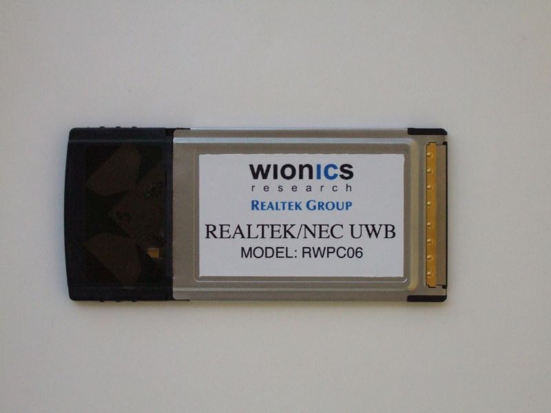
T8YRWPC06UltraWideband PC Card Adapter
Starix Technology, Inc.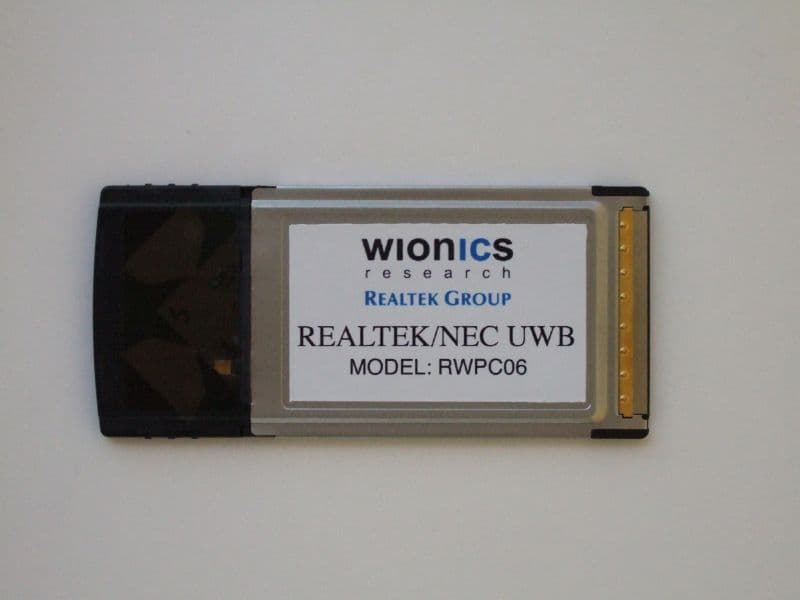
Click to zoom
Application Details
- Equipment Class
- UWB - Ultra Wideband Transmitter
- Date of Grant
- Mar 22, 2007
- Application Purpose
- Original Equipment
- Date of Application
- May 11, 2006
- Equipment Note
- UltraWideband PC Card Adapter
- Frequency Range
- 3100.00000000 - 4800.00000000
- Company
- Starix Technology, Inc.
- Country
- United States
Documents & Files
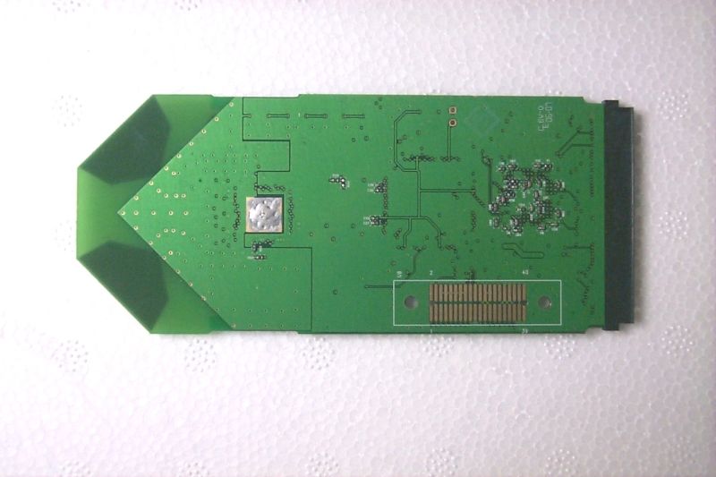
Document Text
Text extracted from the exhibit documents filed with the FCC. Open a document above to read the original.
Users Manual
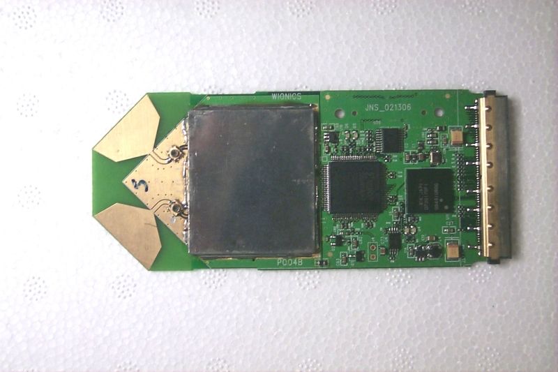
Wionics Research, Realtek Group, Irvine, CA 1 All Rights Reserved by Wionics Research Wionics/NEC Cardbus Demo Board User’s Guide Revision A Wionics Research RealTEK Group Wionics Research, Realtek Group, Irvine, CA 2 All Rights Reserved by Wionics Research Table of Contents 1. Introduction.............................................................................................................3 2. System Description..................................................................................................3 2.1. UWB PHY...................................................................................................4 2.2. FPGA S200..................................................................................................4 2.3. NEC MAC...................................................................................................4 2.4. EEPROM.....................................................................................................4 Wionics Research, Realtek Group, Irvine, CA 3 All Rights Reserved by Wionics Research 1 Introduction This document describes the operations, interfaces, schematic and layout of the Wionics/NEC Cardbus Demo Board. This equipment may only be operated indoors. Operation outdoors is in violation 47 USC 301 and could subject the user to serious legal penalties This device complies with 47 CFR Part 15 of the FCC rules. Operation is subject to 1) this device may not cause harmful interference and 2) this device must accept any interference received, including interference that may cause undesired operation 2 System Description Figure 1 shows the system block diagram of the Wionics/NEC Cardbus Demo Board. UWB PHY UWB PHY FPGA S200 FPGA S200 NEC MAC NEC MAC ANT2 ANT1 MPI_PHYMPI_MAC PHY Debugging & FPGA JTAG Interface PHY Debugging & FPGA JTAG Interface Cardbus Interface Cardbus Interface 512K EEPROM 512K EEPROM MPI_DBG 30MHz Xtal 30MHz Xtal 66MHz OSC 66MHz OSC Figure 1 System Block Diagram The demo system mainly consists of three main chips – (i) UWB PHY, (ii) FPGA S200 and (iii) NEC MAC. Up to two antennas can be supported by the UWB PHY for performance improvement. The existence of FPGA S200 is not necessary for a real product. It serves the purpose of PHY development. The FPGA bridges all the mac-phy interface signals between the NEC MAC and UWB PHY. For the users of the demo board, the FPGA and the PHY debugging interface are transparent in nature. A serial EEPROM is required to store proper data/commands for the PHY chip and MAC chip. To make the system work properly, the EEPROM should be loaded with proper content Wionics Research, Realtek Group, Irvine, CA 4 All Rights Reserved by Wionics Research by using the EEPROM utility provided by NEC. Two basic clock frequencies are used in the system – 30MHz for MAC and 66MHz for PHY. Some more details of the components are shown in the following sections. 2.1 UWB PHY This chip integrates the RF and baseband functions of a UWB PHY defined by the standard organization. This version of PHY chip is packaged in 64 QFN form factor. The analog/RF section requires 1.8V and 3.3V to operate. The digital core operates with 1.5V and the I/O voltage can support a range of 1.8V~3.3V. 2.2 FPGA S200 This is an FPGA chip from Xilinx (XC3S200). When PHY debugging is needed, debugging code will be loaded to the FPGA to bypass the MPI signals to the PHY debugging interface. The problems between MAC and PHY can be isolated during development. In normal operating mode with normal FPGA code loaded, the FPGA is simply transparent to the demo board users. In short, the users do not need to care about detail with the FPGA. Three voltages are required by this chip in the system – 1.2V, 2.5V, 3.3V and VIO (1.8V in this system). 2.3 NEC MAC This MAC chip is from NEC which has a standard MPI interface to communicate with a standard UWB PHY, as well as a standard cardbus/PCI interface to connect directly to a PC. This chip requires a clean analog voltage of 1.5V. Other digital voltages are 1.5V and 3.3V. 2.4 EEPROM This chip is a serial EEPROM from Atmel with a capacity of 512Kb. It is used by the MAC to store the initialization data and command sequence required by the MAC and PHY on start up. This chip requires 3.3V only. shows the PCB stackup and some layer usage information. 3 Software Install • First you should copy the NEC control software (example: UPD720170Utilities_060302.zip) and unzip to a convenient directory. • Plug the PCCard Demo board into the PC. • Found new hardware wizard will automatically start. • When prompted, point the wizard to the Driver sub-directory that you just unzipped. Wionics Research, Realtek Group, Irvine, CA 5 All Rights Reserved by Wionics Research • This should happed a second time. • Now the device will be ready for operation. 4 Software Operation The executable is named FramTest.exe in the bin sub-directory. The application will let you select transmit and receive. For transmit you may select parameters such as channel, data rate and packet length. For spectrum measurements be sure to set a long packet length (longest packet is 4095) and a short packet interval (shortest is 5 usec). A screen shot of the application is in Figure 2. Table 1 shows the correspondence between the application channel selection and the MBOA channel definitions. Figure 2. FramTest application screen shot. Table 1. Channel Selection Table TFC Channel HEX Value 1 9 2 A 3 B 4 C 5 D Wionics Research, Realtek Group, Irvine, CA 6 All Rights Reserved by Wionics Research 6 E 7 F
Block Diagram
Figure 6.6.1: Block diagram of an integrated UWB OFDM PHY tone and symbol deinterl . conv. encoder Viterbi dec . demap QPSK DCM overlap and add 128- point FFT RF TX/RX MAC- PHY inter- face packet detection, frame synch., freq.-off. estimation tone and symbol interl . channel est. and phase tracking A DC D A C map QPSK DCM inverse 128- point FFT + zero prefix upsample and LP filter add pilot tones, add channel est. symbols RSSI AGC, f-hop,... control f-hop,... PLL 1 0 90 PLL 2 0 90 PLL 3 0 90 MUX LPFLPF DAC DAC LPFLPF ADCADC 5 55 5 IV IV RF TUNED Band Select REF Figure 6.6.2: Block diagram of a direct-conversion transceiver L 1 SEL 1 G M L 2 L 3 SEL 2 V LO+ V DD V LO- V LO+ V BB+ V BB- V OUT- V OUT+ From other channel From other channel Figure 6.6.4: Simplified modulator circuit (one channel) and inductive load
Cover Letter(s)
16269 Laguna Canyon Rd. #100 Irvine, California 92618, U.S.A Tel.: (949) 753-5028 Fax.: (949) 753-1329 Letter Of Authorization May 10, 2006 Chief, Authorizations Branch Federal Communications Commission 7435 Oakland Mills Road Columbia, MD 21046 Re: Wionics Certification Application FCC ID: T8YRWPC06 To Whom It May Concern: Please be advised that Wionics Research authorizes TDK R&D Corporation to act on our behalf, until otherwise notified, for the above mentioned application submitted to the Federal Communications Commission (FCC) regarding Ultra-Wideband (UWB) products. We certify that we are not subject to denial of federal benefits, that includes FCC benefits, pursuant to Section 5301 of the Anti-Drug Abuse ACT of 1988, U.S.C. 862. Further, no party, as defined in 47 CFR 1.2002(b), to the application is subject to denial of federal benefits, that includes FCC benefits. Thank you for your attention to this matter. Sincerely, Marc Hill Module Development Manager
Cover Letter(s)
16269 Laguna Canyon Rd. #100 Irvine, California 92618, U.S.A Tel.: (949) 753-5028 Fax.: (949) 753-1329 Request for Confidentiality May 10, 2006 Chief, Authorizations Branch Federal Communications Commission 7435 Oakland Mills Road Columbia, MD 21046 Re: Wionics Certification Application FCC ID: T8YRWPC06 To Whom It May Concern: Wionics Research considers the following materials in its application for certification to be confidential: • Schematics • Bill of Materials • Internal Photos of the unit submitted for tests These technical items we consider to be proprietary and as such any disclosure would be detrimental to our business and our position in the market place. Sincerely, Marc Hill Module Development Manager
Cover Letter(s)
16269 Laguna Canyon Rd., Suite 100, Irvine, California 92618, U.S.A. Tel.: 949-753-5028 Fax 949-753-1329 Confidential and Proprietary Information of Wionics Research Request for Confidentiality Mar 16, 2007 Chief, Authorizations Branch Federal Communications Commission 7435 Oakland Mills Road Columbia, MD 21046 Re: Wionics Certification Application FCC ID: T8YRWPC06 To Whom It May Concern: Wionics Research considers the following materials in its application for certification to be confidential: • Schematics • Bill of Materials These technical items we consider to be proprietary and as such any disclosure would be detrimental to our business and our position in the market place. Sincerely, Child Sun Senior System Engineer
Cover Letter(s)
Wionics Research, Realtek Group, Irvine, CA 1 All Rights Reserved by Wionics Research 1. NEC Cardbus Board/BOM Change Notice (1) Added UWB filters at RF output paths to lower out-of-band emission noise level. (2) Added tuning inductor at radiating channel for flattening in-band signal. (3) Tied digital ground and analog ground together for removal of low frequency spurs.
ID Label/Location Info
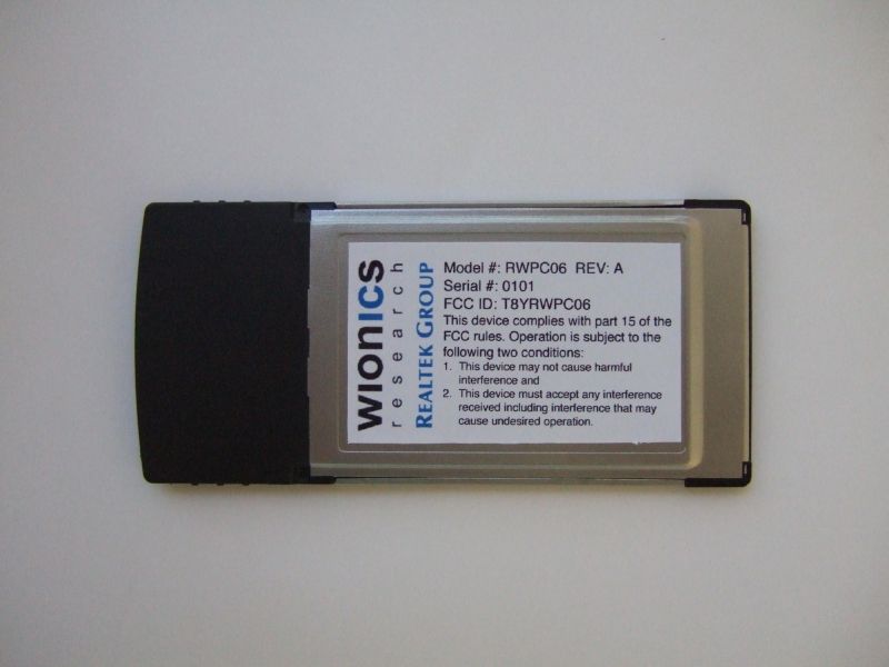
Model Number: RWPC06 Serial Number: 001 FCC ID: T8YRWPC06 This device complies with Part 15 of the FCC rules. Operation is subject to the following two conditions: 1. This device may not cause harmful interference, and 2. This device must accept any interference received, including interference that may cause undesired operation. Model Number: RWPC06 Serial Number: 002 FCC ID: T8YRWPC06 This device complies with Part 15 of the FCC rules. Operation is subject to the following two conditions: 1. This device may not cause harmful interference, and 2. This device must accept any interference received, including interference that may cause undesired operation. Model Number: RWPC06 Serial Number: 003 FCC ID: T8YRWPC06 This device complies with Part 15 of the FCC rules. Operation is subject to the following two conditions: 1. This device may not cause harmful interference, and 2. This device must accept any interference received, including interference that may cause undesired operation. Model Number: RWPC06 Serial Number: 004 FCC ID: T8YRWPC06 This device complies with Part 15 of the FCC rules. Operation is subject to the following two conditions: 1. This device may not cause harmful interference, and 2. This device must accept any interference received, including interference that may cause undesired operation. Model Number: RWPC06 Serial Number: 005 FCC ID: T8YRWPC06 This device complies with Part 15 of the FCC rules. Operation is subject to the following two conditions: 1. This device may not cause harmful interference, and 2. This device must accept any interference received, including interference that may cause undesired operation.
Operational Description
Wionics Research, Realtek Group, Irvine, CA 1 Theory of Operations [1] The transceiver is described in the block diagram of Figure 1. In receive mode, I and Q baseband signals are digitized at 528 MS/s by 5b ADCs. The packet detection and frame synchronization sequence is detected, and appropriate gain settings are provided to the RF transceiver. Channel estimation, phase tracking, and signal demapping is performed after transformation by a 128-point FFT. Different data rates are implemented through variations in the coding rate, coding type, and modulation. Convolutional codes with rates of 1/3, 1/2, 5/8, and 3/4 are supported, along with Dual-Carrier Modulation (DCM) and QPSK modulation. In addition, tone and symbol interleaving improve performance in fading channels. Soft decisions from the demapper are resolved by the Viterbi decoder and the decoded data is output at the MAC/PHY interface. For transmission, the process is reversed, except that I and Q signals sent to the 5b DACs are up-sampled to 1056 MS/s. A clock generation circuit provides clock signals for the digital PHY and data converters. In frequency-hopping mode, a band-select signal provides indication to the RF transceiver of the appropriate operating frequency A block diagram of the direct-conversion RF transceiver is shown in Figure 2. In order to enable agile frequency hopping, this design utilizes three separate RF blocks for each operating frequency in Band Group #1 [2]. Each block consists of a tuned amplifier stage, I/Q mixers, and integer-N frequency synthesizer. In frequency-hopping mode, the appropriate RF block is selected for each OFDM symbol, as indicated by the Band Select signal. Each mixer shares a common output connection to the RX baseband circuitry. Direct-conversion receivers are sensitive to LO carrier leakage. In addition, 13 on-chip linear voltage regulators are employed to provide circuit isolation and further limit coupling through package bondwires. Each voltage regulator design has a programmable output voltage, requires no external components, and occupies 0.007mm 2 . The receiver baseband circuitry is comprised of 5 th -order channel selection filters, PGAs, RSSI circuitry, and DC offset compensation. The fast-frequency hopping in this system places additional constraints on the design of a direct-conversion receiver. AC coupling cannot be employed reliably because DC offsets are in part carrier-frequency dependent, and the fast settling requirement of 9ns in the system prevents resettling of AC coupling circuitry. Furthermore, different frequency bands have different RF path loss parameters, resulting in different receiver gain settings. Therefore, any DC offset correction must remain effective for different gain and carrier frequency settings. The transmitter section employs many of the same concepts as the receiver for implementing frequency hopping. Figure 3 shows a simplified circuit diagram of the modulator circuit (one channel), and the shared switched-inductor load. Capacitors tuned with MOS switches result in high-Q tuning elements, but at the expense of additional parasitic capacitance at the output node. In this system, the 528-MHz channel bandwidth makes the use of high-Q resonant circuits undesirable. The balanced switch configuration used in this design allows the use of a smaller switch for a given parasitic resistance. Furthermore, the parasitic capacitance of the switch is partially transformed by the inductor when referred to the output node. The use of switched inductors also allows Wionics Research, Realtek Group, Irvine, CA 2 each inductor to be optimized separately, potentially allowing a wider operating range than a single inductor, switched-capacitor method. References [1] T. Aytur, et al., ìA Fully Integrated UWB PHY in 0.13 um CMOS,î Proc. ISSCC Conf., San Francisco, pp. 124-125, Feb. 2006 [2] B. Razavi, et al., ìA 0.13-mm CMOS UWB Transceiver,î ISSCC Dig. Tech. Papers, pp. 216-217, Feb. 2005. Figure 1: Block diagram of an integrated UWB OFDM PHY tone and symbol deinterl . conv. encoder Viterbi dec . demap QPSK DCM overlap and add 128- point FFT RF TX/RX MAC- PHY inter- face packet detection, frame synch., freq.-off. estimation tone and symbol interl . channel est. and phase tracking A DC D A C map QPSK DCM inverse 128- point FFT + zero prefix upsample and LP filter add pilot tones, add channel est. symbols RSSI AGC, f-hop,... control f-hop,... PLL 1 0 90 PLL 2 0 90 PLL 3 0 90 MUX LPFLPF DAC DAC LPFLPF ADCADC 5 55 5 IV IV RF TUNED Band Select REF Figure 2: Block diagram of a direct-conversion transceiver L 1 SEL 1 G M L 2 L 3 SEL 2 V LO+ V DD V LO- V LO+ V BB+ V BB- V OUT- V OUT+ From other channel From other channel Figure 3: Simplified modulator circuit (one channel) and inductive load
Test Report
All services undertaken are subject to the following general policy. Reports are submitted for exclusive use of the client to whom they are addressed. Their significance is subject to the adequacy and representative character of the samples and to the comprehensiveness of the tests, examinations or surveys made. This report shall not be reproduced except in full, without written consent of TDK R&D Corporation. This report must not be used to claim product endorsement by A2LA, NVLAP nor any other agency of the US Government. Compliance report of Wionics RWPC06 Customer: Wionics Research Date: January 18, 2007 TDK Report: TTS-TR-T111-107 Test performed by: TDK R&D Corporation 1101 Cypress Creek Rd Cedar Park, TX 78613 Technician Checked by Radiated 30 MHz to 40 GHz A. Medina K. Yata Report A. Medina P. Carson This document contains confidential information and cannot be disclosed outside of Wionics or any affiliated company in whole or in part without the express written permission of TDK R&D Corporation. TTS-TR-T111-107 page 2 of 47 1. Executive Summary An EMC evaluation to determine compliance of the RWPC06 with requirements of FCC 47 CFR Part 15, Subpart F Section 15.519 was conducted. All references are to the most current version of the Code of Federal Regulations 47 that are currently in effect. In accordance with §2.1033, the following data is presented in support of the Certification of the RWPC06. The client should retain a copy of this document on file for at least 5 years after the manufacturing of the product has been discontinued. Test Description FCC 47 CFR Section Compliance Operational Limitations 15.519(a) The client has been notified of these limitations. In normal operating mode the transmitter will only send data when associated with a receiver. See section 5 for detail UWB Bandwidth 15.519(b) Yes Radiated Emissions 15.519(c), 15.209 Yes Radiated Emissions in GPS Bands 15.519(d) Yes Peak Emissions within a 50 MHz Bandwidth 15.519(e) Yes Labelling Requirements 15.519(f) Yes Page 3 of 47 2. Task Description 2.1. Scope Reference FCC ET Docket No. 98-153, FCC 02-48 First R&O; FCC 47 CFR, Part 15, Subpart A; FCC 47 CFR, Part 15, Subpart B; FCC 47 CFR, Part 15, Subpart C; FCC 47 CFR, Part 15, Subpart F FCC ET Docket No. 04-352, Petition for Waiver of the Part 15 UWB Regulations Filed by MBOA-SIG (Adopted: March 10, 2005) Title Revision of Part 15 of the Commission’s Rules Regarding Ultra-Wideband Transmissions Systems; Code of Federal Regulations, Part 15 Subpart A: General Code of Federal Regulations, Part 15 Subpart B: Unintentional Radiators ode of Federal Regulations, Part 15 Subpart C: Intentional Radiators Code of Federal Regulations, Part 15 Subpart F: Ultra-Wideband Operation Purpose of Test To gain FCC Certification for technical requirements for Handheld UWB Systems operating between 3.1 GHz and 10.6 GHz. Test Procedures The tests were conducted in accordance with the following documents: FCC ET Docket 98-153, FCC 02-48 First R&O ANSI C63.4: 2001: Methods of Measurement of Radio-Noise Emissions from Low-Voltage Electrical and Electronic Equipment in the Range of 9 kHz to 40 GHz FCC Code of Federal Regulations 47, Part 15 Subpart A: General FCC ET Docket No. 04-352, Petition for Waiver of the Part 15 UWB Regulations Filed by MBOA-SIG (Adopted: March 10, 2005) General Procedures FCC Code of Federal Regulations 47, Part 2 Frequency Allocations and Radio Treaty Matter: General Rules and Regulations Classification of EUT Hand Held Ultra-Wideband System Page 4 of 47 2.2. Related Submittal(s)/Grant(s) None 2.3. Test Plan Reference Publication Year Title FCC 47 CFR, Part 15, Subpart A 10/2004 Code of Federal Regulations, Part 15 Subpart A: General FCC 47 CFR, Part 15, Subpart B 10/2004 Code of Federal Regulations, Part 15 Subpart B: Unintentional Radiators FCC 47 CFR, Part 15, Subpart C 10/2004 Code of Federal Regulations, Part 15 Subpart C: Intentional Radiators FCC 47 CFR, Part 15, Subpart F 10/2004 Code of Federal Regulations, Part 15 Subpart F: Ultra-Wideband Operation FCC ET Docket 98-153, FCC 02-48 First R&O 04/2002 Revision of Part 15 of the Commission’s Rules Regarding Ultra- Wideband Transmissions Systems: First Report & Order ANSI C63.4 01/2001 Methods of Measurement of Radio- Noise Emissions from Low-Voltage Electrical and Electronic Equipment in the Range of 9 kHz to 40 GHz FCC ET Docket No. 04- 352 3/2005 Petition for Waiver of the Part 15 UWB Regulations Filed by MBOA-SIG 2.4. Client Information APPLICANT Name: Wionics Research Address: 16269 Laguna Canyon Rd Suite 100 Irvine, CA 92618 Contact Person: Child Sun MANUFACTURER Name: Wionics Research Address: 16269 Laguna Canyon Rd Suite 100 Irvine, CA Contact Person: Child Sun Page 5 of 47 2.5. Equipment Under Test (EUT) The following information (with the exception of the date information) has been supplied by the applicant. The test results in this report pertain only to the item tested. General Brand Name Ultra-Wideband Evaluation Kit Product Name Wireless CardBus Reference Design Model Name or Number RWPC06 Serial Number 0101 Type of Equipment UWB Radio Transmitter Input Power Supply Type PC CardBus slot Classification Hand held Ultra-Wideband system Technical Power Supply Requirements Powered through CardBus slot of host PC RF Output Rating -42 dBm EIRP @ 3 meters Operating Frequency Range 3100 MHz to 4800 MHz RF Output Impedance 50 Ω Channel Spacing N/A Pulse Width N/A Pulse Repetition Frequency N/A 10 dB Bandwidth >500 MHz Modulation/Constellation Multiband OFDM Oscillators’ Frequencies 30MHz, 66MHz EUT Ports CardBus Antenna Connector Type Internal Antenna Description Dual Omni directional linear polarized planar Logistics EUT Receive Date December 7, 2006 EUT Receive Condition Good Test Start Date December 8, 2006 Test Completion Date January 12, 2007 Page 6 of 47 2.5.1.Support Equipment Description MFGR Model No. Serial No. FCC ID AC Power Adapter Dell HP-0Q065B83 CN-ON2765-47890- 54E-2669 No ID Laptop P…
Text truncated - open the document above for the full version.
Contact Information
Applicant
Frederic Battaglia(CEO)
Technical Contact
TDK RF SolutionsArmando Medina
[email protected]512 258 9478
1101 Cypress Creek Rd · Cedar Park, Texas · United States
Non-Technical Contact
TDK RF SolutionsPat Carson
[email protected]209 351 1584
Test Firm
TDK RF Solutions, Inc.Robert Sutton
Technical Specifications
| # | Rule Parts | Frequency Range | Power Output |
|---|---|---|---|
| 1 | 15F | 3.10 GHz - 4.80 GHz | - |
Other Applications from Starix Technology, Inc.
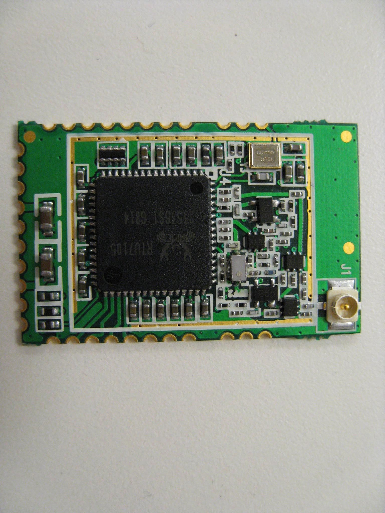
T8YRTU7105-MOD-V3
Nov 12, 2008Wireless USB Module
Equipment Class
UWB - Ultra Wideband Transmitter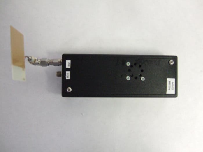
T8YP0029B
Dec 18, 2007One-Port DWA (Device Wire Adapter)
Equipment Class
UWB - Ultra Wideband Transmitter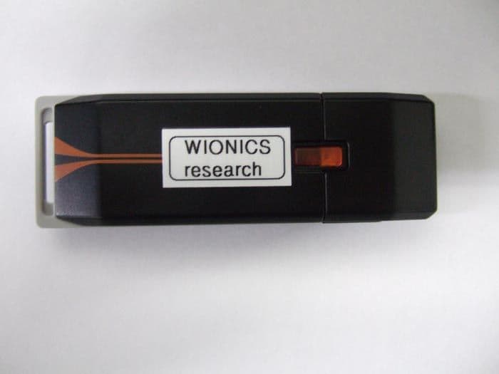
T8YDGLR7CV1
Jul 01, 2007Wireless USB 2.0 Adapter
Equipment Class
UWB - Ultra Wideband Transmitter