TE6DM1800TRANSMITTER-MODULAR APPROVAL
Murata Electronics North America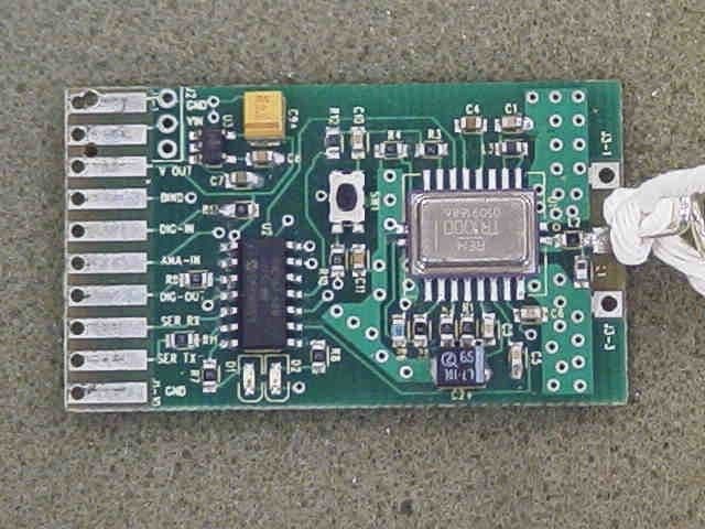
Click to zoom
Application Details
- Equipment Class
- DXX - Part 15 Low Power Communication Device Transmitter
- Date of Grant
- Dec 13, 2005
- Application Purpose
- Original Equipment
- Date of Application
- Dec 13, 2005
- Equipment Note
- TRANSMITTER-MODULAR APPROVAL
- Frequency Range
- 916.30000000 - 916.70000000
- Country
- United States
Documents & Files
Document Text
Text extracted from the exhibit documents filed with the FCC. Open a document above to read the original.
Users Manual
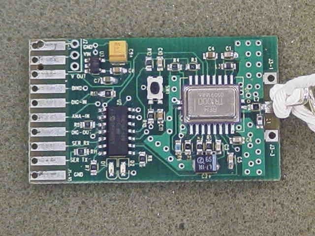
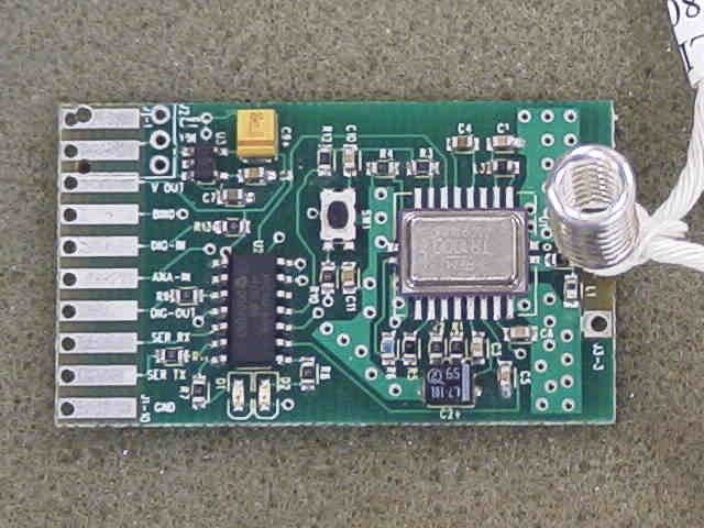
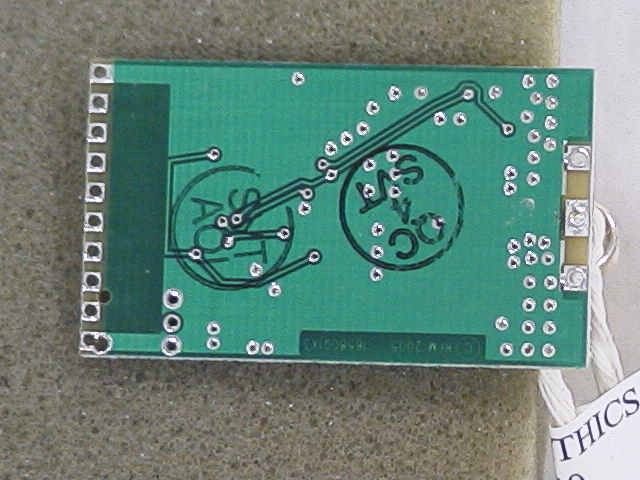
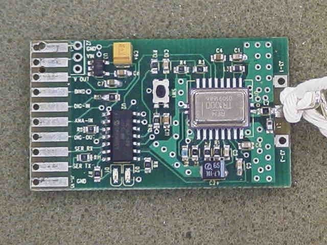
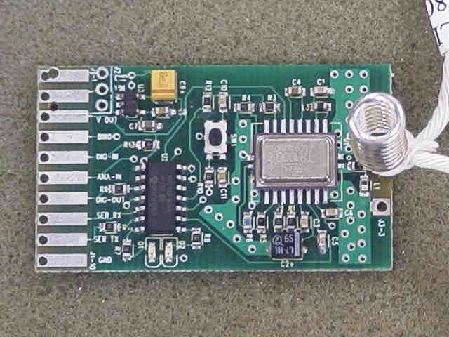
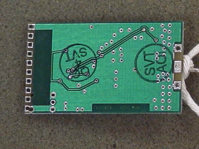
1 ® DM1800- 916MB RatingValueUnits All Input/Output Pins Except VIN-0.3 to +3.3V Non-Operating Ambient Temperature Range-50 to +100 o C Absolute Maximum Ratings Preliminary Electrical Characteristics CharacteristicSymNotesMinimumTypicalMaximumUnits Operating Frequencyf O 916.30916.70MHz Modulation TypeOOK RF Encoded Data Transmission Rate4.8kb/s Average Receiver Input Current, No External Power Supply LoadI R 4mA Receiver Input Signal for 10 -3 BER, 25°C -98dBm Peak Transmitter Input Current, No External Power Supply LoadI TP 13.5mA Peak Transmitter Output PowerP O 1mW Analog Input Measurement Range (10-bit ADC)0VOUTV Source Impedance to Analog Input10K Digital In Logic High2.4V Digital In Logic Low.45V Digital Out Logic High, No Load2.4V Digital In Logic Low, No Load0.3V Digital Output Source Current, 1K load1.1mA Digital Output Sink Current, 1K load1.2mA Serial Port Data Rate9.6kb/s Power Supply Input Voltage Range, -40 to +85 o CVIN2.614V Power Supply Input Voltage Range, 0 to +85 o CVIN3.114V Regulated Power Supply Output Voltage, VIN 3.1 to 14 VVOUT3.0Vdc Regulated Power Supply Voltage Ripple10mV P-P 916.50 MHz Transceiver Module The DM1800-916MB is the 916.50 MHz base station module in the DM1800 family of RF transceiv - ers. The DM1800 family is designed for adding embedded wireless connectivity to a wide range of monitoring and control systems. The DM1800-916MB is equipped with a serial I/O port to interface to a host microcontroller. The module also includes an analog input, a logic input, and a logic output for local monitoring and control. Radio communications range in an “open field” environment is typi - cally 200 meters/hop. The DM1800-916MB combines RFM’s very low current ASH radio technol - ogy with low power microcontroller technology to achieve long battery life. This module is compatible with RFM’s miniMESH TM network protocol, which provides add-on “plug-and-play” multicast mesh network routing. The DM1800-916MB is certified for operation under FCC 15.249 regulations. • Base Station with Host Serial Interface • Compatible with RFM miniMESH TM Network Protocol • 3 V, Very Low Current Operation • Ready-to-Use OEM Module 2 Theory of Operation The major components of the DM1800-916MB include an RFM TR1000 ASH transceiver and a Microchip PIC16F688 microcontroller. The TR1000 operates on a frequency of 916.50 MHz, at a nominal output power of 1 mW. The 16F688 provides a 9.6 kb/s serial interface for communication with a host microcontroller. A compan - ion interface board is available with USB bridge cir - cuitry to interface the DM1800-916MB to a host PC. Three of the 16F688 I/O pins are configured for exter - nal monitoring or control.Digital Inis configured as a logic input with a weak pull-up for sensing a contact closure to a ground pad.Digital Outis configured a logic output.Analog Inis configured as a 10-bit ana - log-to-digital input. The DM1800 includes two LEDs that indicate the module’s operating mode. The DM1800-916MB is compatible with RFM’s miniMESH TM network protocol, which provides add-on “plug-and-play” mesh network routing to improve com - munication range and robustness. DM1800-916MB FCC Certification The DM1800-916MB hardware has been certified for operation under FCC Part 15 Rules, Section 15.249. This certification applies only when a DM1800-916MB is equipped with one of the following RFM antennas: helical antenna, RFM part number 500-1195-003 helical antenna, RFM part number 500-1195-103 WARNING: the DM1800-916MB must be re-certified if used with any antennas other than the two listed above.Contact RFM for further information if your ap - plication requires a special antenna configuration. FCC Notices and Labels This device complies with Part 15 of the FCC rules. Operation is subject to the following two conditions: (1) this device may not cause harmful interference, and (2) this device must accept any interference re - ceived, including interference that may cause unde - sired operation. A clearly visible label is required on the outside of the user’s (OEM) enclosure stating that this product con - tains a DM1800-916MB transceiver assembly, FCC ID: TE6-DM1800. WARNING: This device operates under Part 15 of the FCC rules. Any modification to this device, not ex- pressly authorized by RF Monolithics, Inc., may void the user’s authority to operate this device. TXMOD RX DATA CNTRL1 CNTRL0 PIC 16F688 μP DM1800-916MB Block Diagram LED 1 LED 2 ASH Transceiver GND SERIAL TX SERIAL RX DIGITAL OUT ANALOG IN DIGITAL IN BIND GND VOUT VIN 3 V Reg GND GND J1-1 J1-2 J1-3 J1-4 J1-5 J1-6 J1-7 J1-8 J1-9 J1-10 J2-2 J2-1 J2-3 Figure 1 PinNameDescription J1-1GNDThis pad is a signal and power supply ground. J1-2VINThis is the power supply input pad. The allowed input voltage range is 2.6 to 14 V. J1-3VOUT VOUT tracks 50 to 100 mV below VIN when VIN is in the range of 2.6 to 3.1 V. When VIN is in the range of 3.1 to 14 V, VOUT is regulated at 3.0 Vdc. Up to 10 mA can be supplied from this pad for powering external circuits such as thermistor-resistor networks. External circuitry must not impress more than 10 mV p-p ripple on the regu - lated output voltage. J1-4BIND This pad is connected to a logic input on the microcontroller, and is configured with a weak pull-up. When this pin is momentarily grounded (to J1-1 or J1-10, the module is placed into the bind mode, allowing this module to be associated with other modules to form a network. J1-5DIGITAL IN This pad is connected to a logic input on the microcontroller, and is configured with a weak pull-up, allowing both logic signals and contact closures referenced to J-1 or J-10 to be read. The value of this input is sent over the RF channel as a response to an RF command. The input voltage range on this pad is 0 to VOUT. Applying a voltage outside of this range may damage the module. J1-6ANALOG IN This pad in the input to the microcontroller’s 10-bit analog-to-digital (ADC) converter. The ADC input range is 0 to VOUT, refere…
Text truncated - open the document above for the full version.
Cover Letter(s)
849 NW State Road 45 • P. O. Box 370 • Newberry, Florida 32669 USA Telephone (352) 472-5500 • (888) 472-2424 • FAX (352) 472-2030 • email: [email protected] December 5, 2005 Federal Communications Commission Authorization and Evaluation Division 7435 Oakland Mills Road Columbia, MD 21046 Ref.: RF Monolithics, Inc.’s Application for Modular Approval on their FCC ID: TE6DM1800 To Whom It May Concern: Enclosed please find an application for Modular Approval for RF Monolithics, Inc.’s FCC ID: TE6-DM1800. The attached test report will show that this device meets the requirements for modular approval per DA 00-1407 dated June 26, 2000. Should you have any questions or require any further information, please advise. Regards, Mario R. de Aranzeta Enclosure
Cover Letter(s)
te6cm2201n.doc 1 of 1 December 12, 2005 Federal Communications Commission Authorization and Evaluation Division Confidentiality Request regarding application for certification of FCC ID: TE6DM1800 Pursuant to Sections 0.457 and 0.459 of the Commission’s Rules, we hereby request confidential treatment of information accompanying this application as outlined below: Schematics Block Diagram The above materials contain trade secrets and proprietary information not customarily released to the public. The public disclosure of these materials may be harmful to the applicant and provide unjustified benefits to its competitors. The applicant understands that pursuant to Section 0.457 of the Rules, disclosure of this application and all accompanying documentation will not be made before the date of the Grant for this application. Sincerely, RF Monolithics, Inc. Terry Hinkle Director of Module Products ® RF Monolithics, Inc. 4441 Sigma Road Dallas, TX 75244 USA Phone: (972) 448-3700 Fax: (972) 387-8148 Web: http://www.rfm.com
ID Label/Location Info
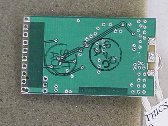
FCC ID LABEL SAMPLE: FCC Label Location FCC ID: TE6DM1800
ID Label/Location Info
FCC ID LABEL SAMPLE: FCC Label Location FCC ID: TE6DM1800
Operational Description
2 Theory of Operation The major components of the DM1800-916MB include an RFM TR1000 ASH transceiver and a Microchip PIC16F688 microcontroller. The TR1000 operates on a frequency of 916.50 MHz, at a nominal output power of 1 mW. The 16F688 provides a 9.6 kb/s serial interface for communication with a host microcontroller. A compan - ion interface board is available with USB bridge cir - cuitry to interface the DM1800-916MB to a host PC. Three of the 16F688 I/O pins are configured for exter - nal monitoring or control.Digital Inis configured as a logic input with a weak pull-up for sensing a contact closure to a ground pad.Digital Outis configured a logic output.Analog Inis configured as a 10-bit ana - log-to-digital input. The DM1800 includes two LEDs that indicate the module’s operating mode. The DM1800-916MB is compatible with RFM’s miniMESH TM network protocol, which provides add-on “plug-and-play” mesh network routing to improve com - munication range and robustness. DM1800-916MB FCC Certification The DM1800-916MB hardware has been certified for operation under FCC Part 15 Rules, Section 15.249. This certification applies only when a DM1800-916MB is equipped with one of the following RFM antennas: helical antenna, RFM part number 500-1195-003 helical antenna, RFM part number 500-1195-103 WARNING: the DM1800-916MB must be re-certified if used with any antennas other than the two listed above.Contact RFM for further information if your ap - plication requires a special antenna configuration. FCC Notices and Labels This device complies with Part 15 of the FCC rules. Operation is subject to the following two conditions: (1) this device may not cause harmful interference, and (2) this device must accept any interference re - ceived, including interference that may cause unde - sired operation. A clearly visible label is required on the outside of the user’s (OEM) enclosure stating that this product con - tains a DM1800-916MB transceiver assembly, FCC ID: TE6-DM1800. WARNING: This device operates under Part 15 of the FCC rules. Any modification to this device, not ex- pressly authorized by RF Monolithics, Inc., may void the user’s authority to operate this device. TXMOD RX DATA CNTRL1 CNTRL0 PIC 16F688 μP DM1800-916MB Block Diagram LED 1 LED 2 ASH Transceiver GND SERIAL TX SERIAL RX DIGITAL OUT ANALOG IN DIGITAL IN BIND GND VOUT VIN 3 V Reg GND GND J1-1 J1-2 J1-3 J1-4 J1-5 J1-6 J1-7 J1-8 J1-9 J1-10 J2-2 J2-1 J2-3 Figure 1
Test Report
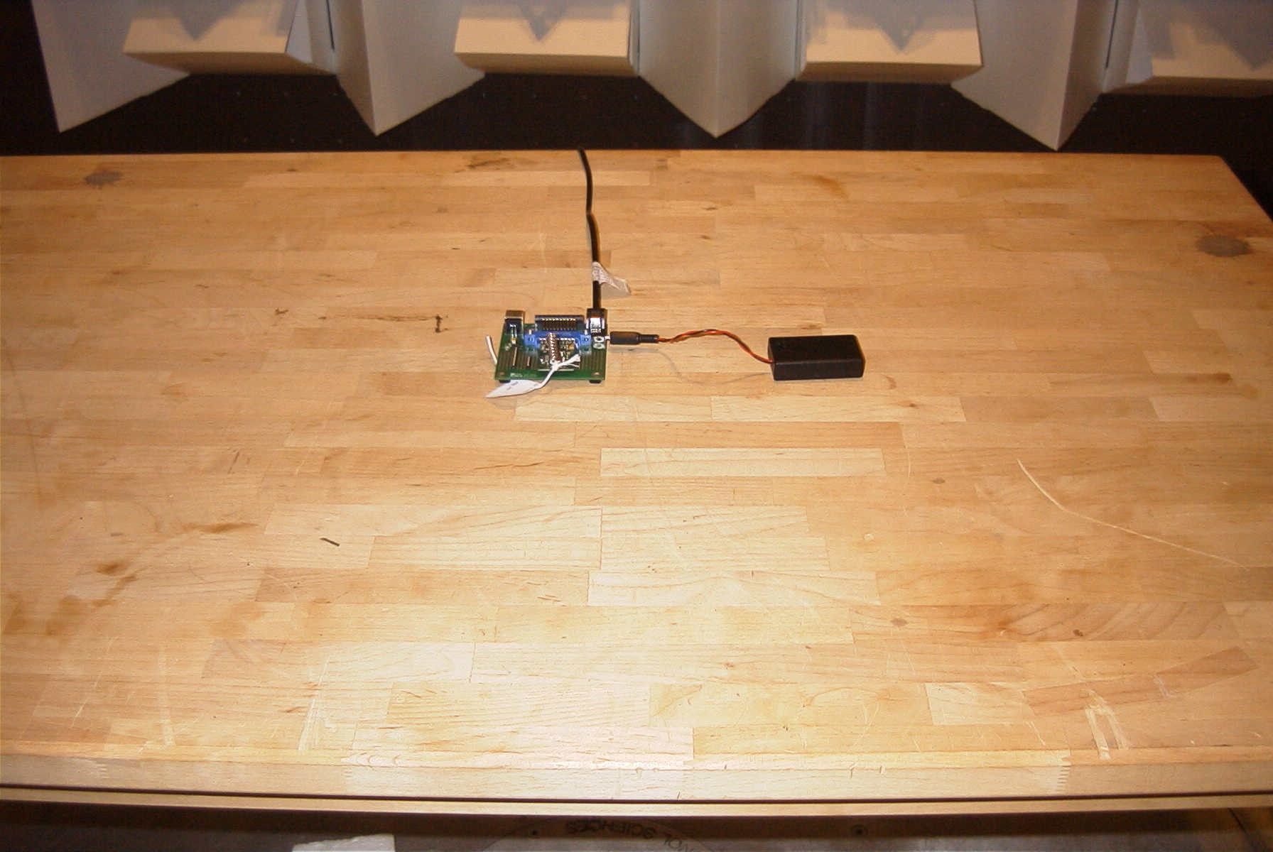
TIMCO ENGINEERING INC. 849 NW State Road 45 Newberry, Florida 32669 http://www.timcoengr.com 888.472.2424 F 352.472.2030 email: [email protected] APPLICANT: RF MONOLITHICS, INC. FCC ID: TE6DM1800 Test Report Product Name: TRANSMITTER-MODULAR APPROVAL FCC ID: TE6DM1800 Applicant: RF MONOLITHICS, INC. 4441 SIGMA ROAD DALLAS TX 75244 USA Date Receipt: 11/8/2005 Date Tested: 11/16/2005 REPORT #: R\RF MONOLITHICS TE6\2260AUT5\2260AUT5TestReport.doc COVER SHEET TIMCO ENGINEERING INC. 849 NW State Road 45 Newberry, Florida 32669 http://www.timcoengr.com 8.472.2424 F 352.472.2030 email: [email protected] APPLICANT: RF MONOLITHICS, INC. FCC ID: TE6DM1800 REPORT #: R\RF MONOLITHICS TE6\2260AUT5\2260AUT5TestReport.doc TABLE OF CONTENTS 88 APPLICANT: RF MONOLITHICS, INC. FCC ID: TE6DM1800 TABLE OF CONTENTS TEST REPORT CONTAINING: PAGE 1-2.........MODULAR REQUIREMENTS PAGE 3...........TEST EQUIPMENT LIST PAGE 4...........TEST PROCEDURE PAGE 5-6.........RADIATION INTERFERENCE TEST DATA PAGE 7...........DUTY CYCLE PLOT PAGE 8...........OCCUPIED BANDWIDTH PAGE 9...........OCCUPIED BANDWIDTH PLOT EXHIBIT INCLUDED: REQUEST FOR CONFIDENTIALITY LETTER COVER LETTER REQUESTING MODULAR APPROVAL BLOCK DIAGRAM SCHEMATIC USERS MANUAL LABEL SAMPLE LABEL LOCATION PHOTOGRAPHS OPERATIONAL DESCRIPTION TEST SET UP PHOTOGRAPH TIMCO ENGINEERING INC. 849 NW State Road 45 Newberry, Florida 32669 http://www.timcoengr.com 888.472.2424 F 352.472.2030 email: [email protected] APPLICANT: RF MONOLITHICS, INC. FCC ID: TE6DM1800 MODULAR REQUIREMENTS 1. The modular transmitter must have its own RF shielding. All of the transceiver RF portions are in a hermetically sealed case on the top surface of the module. 2. The modular transmitter must have buffered modulation data inputs. The transmitter has a modulated buffer amplifier for data transmission. See the operational description exhibit. 3. The modular transmitter must have its own power supply regulation. The schematic for this unit shows on-board regulators. 4. The modular transmitter must comply with the antenna requirements of Section 15.203 and 15.204(c). The module is being certified with a helically wound wire resonate antenna at 916.4 MHz. It will be sold with it placed vertically on the board and horizontally on the board. It was tested in both configurations and the data is included in the test report. 5. The modular transmitter must be tested in a stand-alone configuration. The DM1800 was tested in a stand alone configuration. See the test setup photographs. 6. The modular transmitter must be labeled with its own FCC ID number. The FCC ID Label Sample and Label Location are included in the exhibits. REPORT #: U:\R\RF MONOLITHICS TE6\2260AUT5\2260AUT5TestReport.doc Page 1 of 9 TIMCO ENGINEERING INC. 849 NW State Road 45 Newberry, Florida 32669 http://www.timcoengr.com 888.472.2424 F 352.472.2030 email: [email protected] APPLICANT: RF MONOLITHICS, INC. FCC ID: TE6DM1800 MODULAR REQUIREMENTS CONTD. 7. The modular transmitter must comply with any specific rule or operating requirements applicable to the transmitter. The DM1800 meets all of the requirements per FCC Rules Part 15.249 and data is included in the report. 8. The modular transmitter must comply with any applicable RF exposure requirements. The unit is of such low power it meets all RF Exposure requirements. REPORT #: U:\R\RF MONOLITHICS TE6\2260AUT5\2260AUT5TestReport.doc Page 2 of 9 TIMCO ENGINEERING INC. 849 NW State Road 45 Newberry, Florida 32669 http://www.timcoengr.com 888.472.2424 F 352.472.2030 email: [email protected] APPLICANT: RF MONOLITHICS, INC. FCC ID: TE6DM1800 EMC Equipment List Device Manufacturer Model Serial Number Cal/Char Date Due Date 3/10-Meter OATS TEI N/A N/A Listed 3/27/04 3/26/07 3-Meter OATS TEI N/A N/A Listed 1/13/03 1/12/06 Biconnical Antenna Eaton 94455-1 1096 CAL 8/17/04 8/17/06 Biconnical Antenna Electro- Metrics BIA-25 1171 CAL 4/29/05 4/29/07 Blue Tower Quasi-Peak Adapter HP 85650A 2811A01279 CAL 4/13/05 4/13/07 Blue Tower RF Preselector HP 85685A 2926A00983 CAL 8/3/05 8/3/07 Blue Tower Spectrum Analyzer HP 8568B 2928A04729 2848A18049 CAL 4/13/05 4/13/07 LISN Electro- Metrics ANS-25/2 2604 CAL 8/27/04 8/27/06 LISN Electro- Metrics EM-7820 2682 CAL 4/28/05 4/28/07 Log- Periodic Antenna Eaton 96005 1243 CAL 5/8/05 5/8/07 REPORT #: U:\R\RF MONOLITHICS TE6\2260AUT5\2260AUT5TestReport.doc Page 3 of 9 TIMCO ENGINEERING INC. 849 NW State Road 45 Newberry, Florida 32669 http://www.timcoengr.com 888.472.2424 F 352.472.2030 email: [email protected] APPLICANT: RF MONOLITHICS, INC. FCC ID: TE6DM1800 TEST PROCEDURE GENERAL: This report shall NOT be reproduced except in full without the written approval of TIMCO ENGINEERING, INC. The UUT was transmitting a test signal during the testing. RADIATION INTERFERENCE: The test procedure used was ANSI STANDARD C63.4-2003 using a HEWLETT PACKARD spectrum analyzer with a pre-selector. The analyzer was calibrated in dB above a microvolt at the output of the antenna. The resolution bandwidth was 100KHz and the video bandwidth was 300KHz up to 1.0GHz and 1.0MHz with a video BW of 3.0MHz above 1.0GHz. The ambient temperature of the UUT was 74.3°F with a humidity of 69%. FORMULA OF CONVERSION FACTORS: The Field Strength at 3m was established by adding the meter reading of the spectrum analyzer (which is set to read in units of dBuV) to the antenna correction factor supplied by the antenna manufacturer. The antenna correction factors are stated in terms of dB. The gain of the Preselector was accounted for in the Spectrum Analyzer Meter Reading. Example: Freq (MHz) METER READING + ACF = FS 33 20 dBuV + 10.36 dB = 30.36 dBuV/m @ 3m ANSI STANDARD C63.4-2003 10.1.7 MEASUREMENT PROCEDURES: The UUT was placed on a table 80 cm high and with dimensions of 1m by 1.5m. The UUT was placed in the center of the table (1.5m side). The table used for radiated measurements is capable of continuous rotation. When an emission was found, the table was rotated to produce the ma…
Text truncated - open the document above for the full version.
Contact Information
Applicant
Mark Tucker(Manager, Hardware Engineering Group)
Test Firm
Timco Engineering, Inc.Sid Sanders
Technical Specifications
| # | Rule Parts | Frequency Range | Power Output |
|---|---|---|---|
| 1 | 15C | 916.3 MHz - 916.7 MHz | - |
Other Applications from Murata Electronics North America
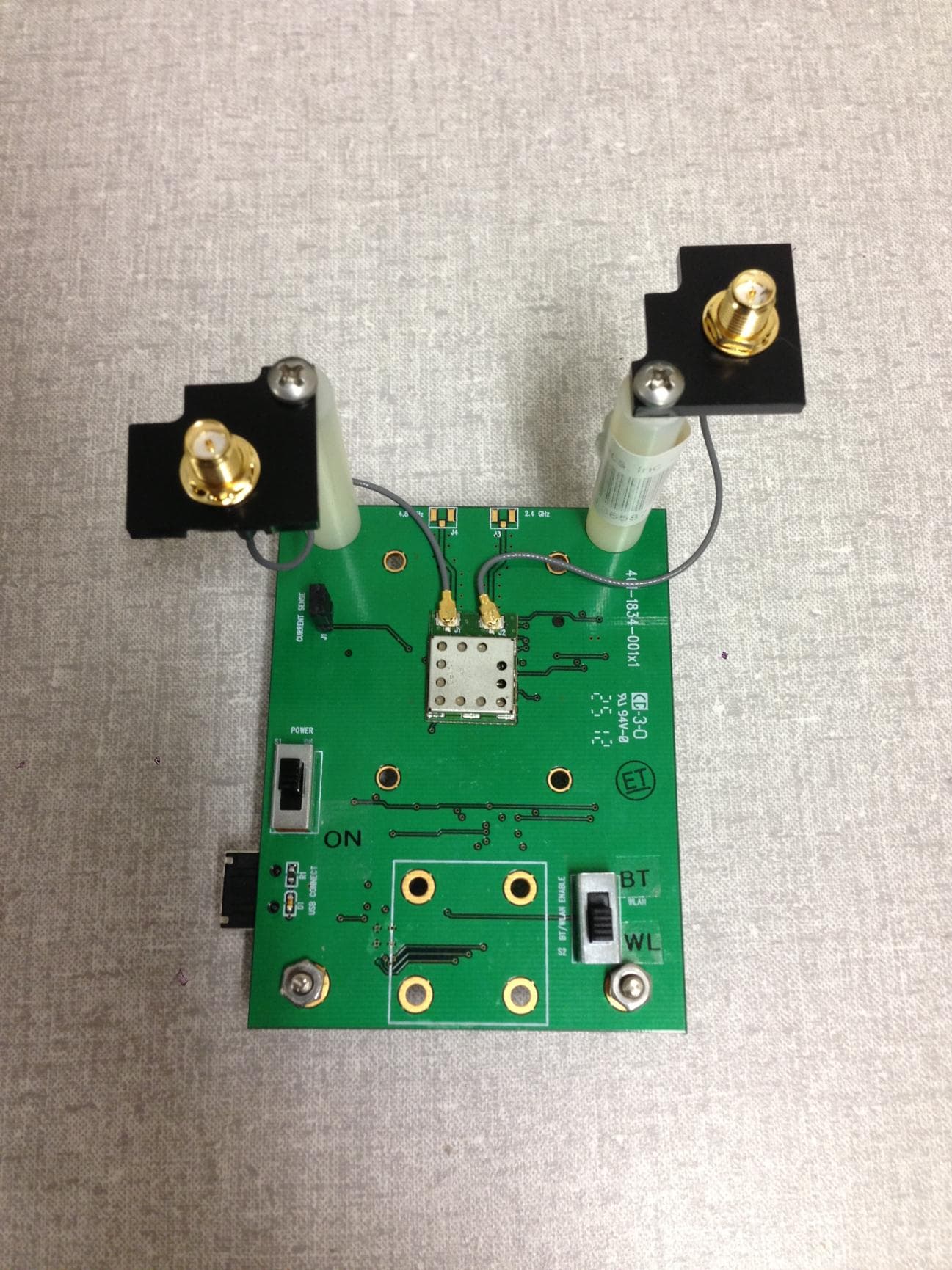
TE6-DRWLS1273L
Dec 16, 2012DR-WLS1273L-102
Equipment Class
DTS - Digital Transmission System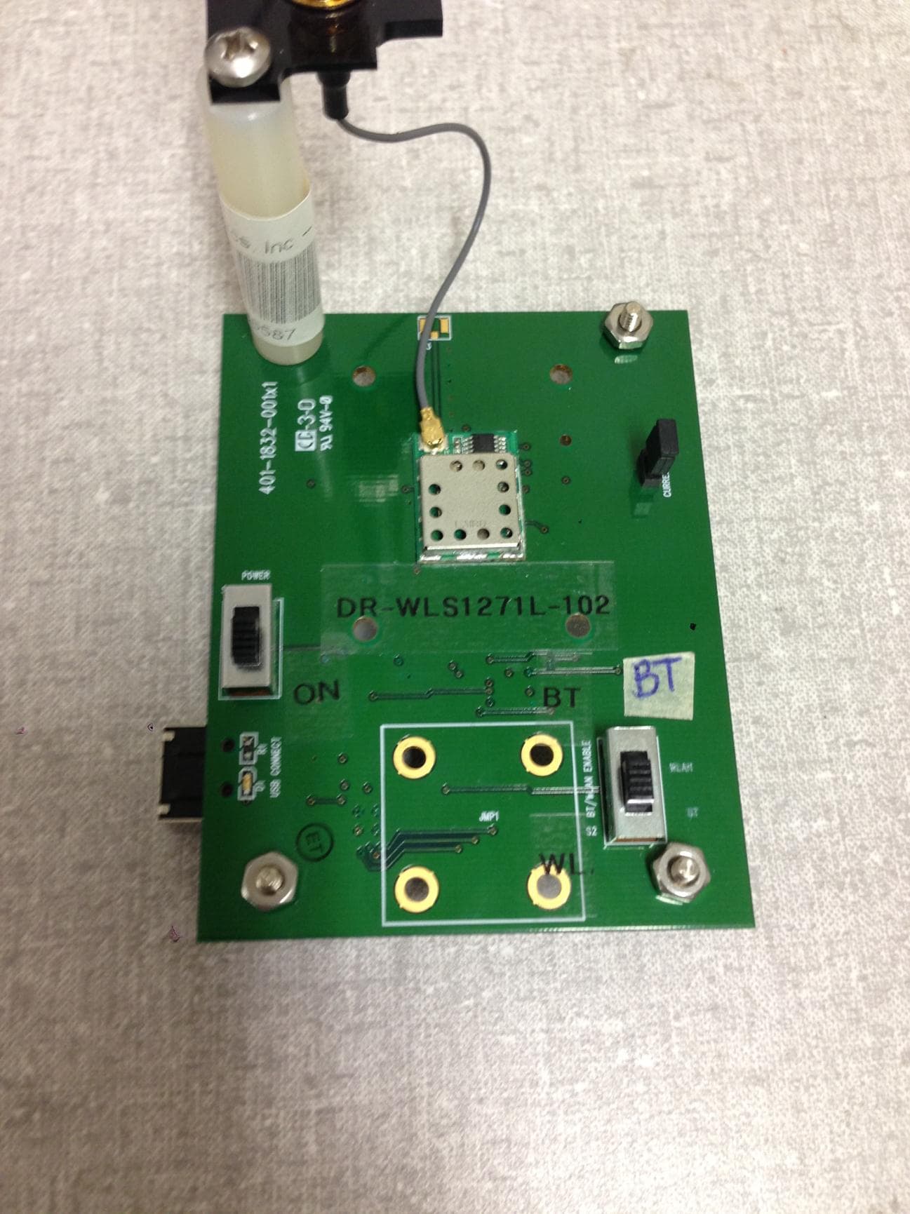
TE6-DRWLS1271L
Dec 16, 2012DR-WLS1271L-102
Equipment Class
DSS - Part 15 Spread Spectrum Transmitter
TE6-DM2200A
May 15, 2006Remote Transceiver Module
Equipment Class
DTS - Digital Transmission System
TE6CM2202N
Mar 16, 2006Remote Data Transmitter
Equipment Class
DXX - Part 15 Low Power Communication Device Transmitter
TE6-CM2201N
Nov 02, 2005TRANSCEIVER MODULE
Equipment Class
DXX - Part 15 Low Power Communication Device Transmitter