TFJA10-T-GMPayment Terminal
Uniform Industrial Corp.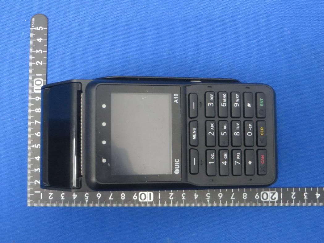
Click to zoom
Application Details
- Equipment Class
- PCB - PCS Licensed Transmitter
- Date of Grant
- Jan 06, 2021
- Application Purpose
- Original Equipment
- Date of Application
- Jan 04, 2021
- Equipment Note
- Payment Terminal
- Frequency Range
- 699.70000000 - 715.30000000
- Company
- Uniform Industrial Corp.
- Country
- United States
Documents & Files
Document Text
Text extracted from the exhibit documents filed with the FCC. Open a document above to read the original.
Users Manual
A10T manual Page 1 Payment Terminal A10-T The A10-T is a compact payment terminal, designed to support financial inclusion scenarios as well as innovative payment schemes in mature markets. Specification Processor Microchip SAMA5D28 Memory DDR2 128MB Storage Flash 256MB Display 2.8” IPS 320x240 OS Linux Audio Buzzer (Default) Speaker x1 (PCBA Reserved) Buzzer Sound Pressure Level:70 dB/10cm(2.5KHz) Reader Magnetic Card Reader Bi-directional, support triple tracks ISO7811 Speed 5 to 40 IPS 1,000,000. swipe times Smart Card Reader ISO7816, T=0 , T=1 EMV Level 1, Support 5V/3V 500,000. inserted times Contactless ISO14443A&B, MIFARE HW Ready for NFC Printer 384dots/lines,105mm/s paper roll 58mm x Ø 40 mm paper thickness 60-80um 3G/4G (optional) ME3630 (for FCC ID: TFJA10-T-ME) GM500-U1A (for FCC ID: TFJA10-T-GM) I/O Connector RJ11 RS232 x1 RI (as VCC5V/9V by cable), Baud rate 115200 bps RJ11 RS232 x1 RI (as VCC 9V), RTS/CTS, Baud rate 115200 bps Modem x1(default) V.92, V.32bis, V80 14400, 12000, 9600,7200 BPS RJ45 x1 (Ethernet) 10BASE-T/100BASE-T USB USB1 x1 Host USB2 x1 Host\Device (detect pin) (USB port A for SAMBA) USB2.0 A10T manual Page 2 DC Jack x1 SAM X0, x4(optional) SIM x1 (optional) Debug console 2.54mm Head X1(2pin) LED indicator Mono, Green X4 for EMV Keypad Rubber Keys *18 (Func. keys*3, STD Keys *15) Environment Operating Temperature 0°C to +40°C Storage Temperature -20°C to +70°C Humidity 5% to 90% Reliability Requirements MTBF 100,000 hours Drop test 76 cm without damage ESD Air:+/-15KV Contact:+/- 8KV Key button 1M times Battery Life 5 years SW requirement EMV card Logo Card brand logo on LCD Installation guide (USB Interface) 1 Plug the adapter. 2 Plug the USB cable to the USB port of PC. 3 Install the driver A10T manual Page 3 A10T manual Page 4 FEDERAL COMMUNICATIONS COMMISSION INTERFERENCE STATEMENT This equipment has been tested and found to comply with the limits for a Class B digital device, pursuant to part 15 of the FCC Rules. These limits are designed to provide reasonable protection against harmful interference in a residential installation. This equipment generates, uses and can radiate radio frequency energy and, if not installed and used in accordance with the instructions, may cause harmful interference to radio communications. However, there is no guarantee that interference will not occur in a particular installation. If this equipment does cause harmful interference to radio or television reception, which can be determined by turning the equipment off and on, the user is encouraged to try to correct the interference by one or more of the following measures: -Reorient or relocate the receiving antenna. -Increase the separation between the equipment and receiver. -Connect the equipment into an outlet on a circuit different from that to which the receiver is connected. -Consult the dealer or an experienced radio/ TV technician for help. CAUTION: Any changes or modifications not expressly approved by the grantee of this device could void the user's authority to operate the equipment. This device complies with Part 15 of the FCC Rules. Operation is subject to the following two conditions: (1) this device may not cause harmful interference, and (2) this device must accept any interference received, including interference that may cause undesired operation. RF Exposure Information (SAR) This device meets the government’s requirements for exposure to radio waves. This device is designed and manufactured not to exceed the emission limits for exposure to radio frequency (RF) energy set by the Federal Communications Commission of the U.S. Government. The exposure standard employs a unit of measurement known as the Specific Absorption Rate, or SAR. The SAR limit set by the FCC is 1.6 W/kg. Tests for SAR are conducted using standard operating positions accepted by the FCC with the EUT transmitting at the specified power level in different channels.
External Photos
Report No.: 2011RSU040-UE 1 of 6 EUT External Photograph (1) EUT Photo (2) EUT Photo Report No.: 2011RSU040-UE 2 of 6 (3) EUT Photo (4) EUT Photo Report No.: 2011RSU040-UE 3 of 6 (5) EUT Photo (6) EUT Photo Report No.: 2011RSU040-UE 4 of 6 (7) EUT Photo (8) EUT Photo Report No.: 2011RSU040-UE 5 of 6 (9) EUT Photo (10) EUT Photo Report No.: 2011RSU040-UE 6 of 6 (11) EUT Photo
External Photos
Report No.: 2011TW5402-U2~U7 Product: Payment Terminal Brand Name: UIC Model Number: A10-T 1 of 11 External Photograph (1) EUT Photo (A10-T) (2) EUT Photo (A10-T) Report No.: 2011TW5402-U2~U7 2 of 11 (3) EUT Photo (A10-T) (4) EUT Photo (A10-T) Report No.: 2011TW5402-U2~U7 3 of 11 (5) EUT Photo (A10-T) (6) EUT Photo (A10-T) Report No.: 2011TW5402-U2~U7 4 of 11 (7) EUT Photo (A10-T) (8) Adapter (PA1050-090T1A500) Report No.: 2011TW5402-U2~U7 5 of 11 (9) Adapter (PA1050-090T1A500) (10) Adapter (PA1050-090T1A500) Report No.: 2011TW5402-U2~U7 6 of 11 (11) Adapter (PA1050-090T1A500) (12) Adapter (PA1050-090T1A500) Report No.: 2011TW5402-U2~U7 7 of 11 (13) Adapter (PA1050-090T1A500) (14) Adapter (PA1050-090T1A500) Report No.: 2011TW5402-U2~U7 8 of 11 (15) Adapter (BA048-090500MAX) (16) Adapter (BA048-090500MAX) Report No.: 2011TW5402-U2~U7 9 of 11 (17) Adapter (BA048-090500MAX) (18) Adapter (BA048-090500MAX) Report No.: 2011TW5402-U2~U7 10 of 11 (19) Adapter (BA048-090500MAX) (20) Adapter (BA048-090500MAX) Report No.: 2011TW5402-U2~U7 11 of 11 (21) Adapter (BA048-090500MAX) (22) EUT Photo (Power Cable)
ID Label/Location Info
Label Label Location
Internal Photos
Report No.: 2011TW5402-U2, U4, U6 Product: Payment Terminal Brand Name: UIC Model Number: A10-T 1 of 13 Internal Photograph (1) EUT Photo (2) EUT Photo Report No.: 2011TW5402-U2, U4, U6 2 of 13 (3) EUT Photo (4) EUT Photo Report No.: 2011TW5402-U2, U4, U6 3 of 13 (5) EUT Photo (6) EUT Photo Report No.: 2011TW5402-U2, U4, U6 4 of 13 (7) EUT Photo (8) EUT Photo Report No.: 2011TW5402-U2, U4, U6 5 of 13 (9) EUT Photo (10) EUT Photo Report No.: 2011TW5402-U2, U4, U6 6 of 13 (11) EUT Photo (12) EUT Photo Report No.: 2011TW5402-U2, U4, U6 7 of 13 (13) EUT Photo (14) EUT Photo Report No.: 2011TW5402-U2, U4, U6 8 of 13 (15) EUT Photo (16) EUT Photo Report No.: 2011TW5402-U2, U4, U6 9 of 13 (17) EUT Photo (18) EUT Photo Report No.: 2011TW5402-U2, U4, U6 10 of 13 (19) EUT Photo (20) EUT Photo Report No.: 2011TW5402-U2, U4, U6 11 of 13 (21) EUT Photo (22) EUT Photo Report No.: 2011TW5402-U2, U4, U6 12 of 13 (23) EUT Photo (24) EUT Photo Report No.: 2011TW5402-U2, U4, U6 13 of 13 (25) EUT Photo (26) EUT Photo
Operational Description
Operation Description FCC ID: TFJA10-T-GM This device(Payment Terminal contains RFID(13.56MHz) and WWAN module which GOSUNCN GM500-U1A is designed to provide customers with global network coverage on the connectivity of LTE. It delivers 50Mbps upload and 150Mbps download data rates on LTE networks and can also be fully backward compatible with existing 3G networks.GM500-U1A is P2P with ME3630 series. Rx diversity which allows the end-device to be equipped with two distinct cellular antennas improving the quality and reliability of the wireless connectivity. A rich set of internet protocols (PAP and CHAP used for PPP connections)and abundant functions (GNSS, Remote wakeup, TCP/UDP, FTP, HTTP, SMS) extend the applicability of the module to a wide range of M2M applications. GM500-U1A also allows the integration of automotive and other applications requiring assured extended operating temperature range and mechanical ruggedness within the ever-shrinking space inside electronic bays in trucks, automobiles, and other mobile platforms. Feature Implementation Electrical & Sensitivity Power –LTE: 23 ±2.7dBm (Power Class 3) –WCDMA : 24 +1/-3dBm (Power Class 3) –RFID Receiving sensitivity: -Rx Diversity Data Features : LTE FDD (CAT4) – Uplink 50Mbps / Downlink 150 Mbps LTE TDD (CAT4) – Uplink30Mbps / Downlink 112Mbps WCDMA – Uplink 5.76Mbps / Downlink 42Mbps Modulations : 3G/4G: UPLink : QPSK/16QAM ; Downlink : QPSK/16QAM/64QAM RFID : ASK Antenna gain : band 2: 1.75dBi , Band4: 1.07dBi, Band 5: 3.68dBi, Band 12: 0.75dBi Antenna TYPE: FPCB Frequency: RFID : 13.56MHz WCDMA: B2:1850MHz~1910MHz ; B5:1710MHz~1755MHz ; LTE: B2:1850MHz~1910MHz ; B4:1710MHz~1755MHz ; B5:1710MHz~1755MHz ; B12:699MHz~716MHz
RF Exposure Info
MRT Technology (Suzhou) Co., Ltd Report No.: 2011RU040-U1 Phone: +86-512-66308358 Report Version: V01 Web: www.mrt-cert.com Issue Date: 12-04-2020 Page Number: 1 of 80 FCC ID: TFJA10-T-GM Applicant: Uniform Industrial Corp. Application Type: Certification Product: Payment Terminal Model No.: A10-T Module: GM500-U1A Brand Name: UIC FCC Classification: Wireless Wide Area Network (WWAN) FCC Rule Part(s): FCC 47 CFR Part 2.1093 Test Procedure(s): IEEE 1528:2013; IEEE C95.1- 2005; KDB 447498 D01v06; KDB 865664 D01v01r04; KDB 941225 D01v03r01; KDB 941225 D05v02r05 Test Date: December 01 ~ 02, 2020 SAR MEASUREMENT REPORT Reviewed By: ( Kevin Guo ) Approved By: ( Robin Wu ) The test results relate only to the samples tested. This equipment has been shown to be capable of compliance with the applicable technical standards as indicated in the measurement report and was tested in accordance with the measurement procedures specified in IEEE1528, KDB 447498 and KDB 865664. Test results reported herein relate only to the item(s) tested. The test report shall not be reproduced except in full without the written approval of MRT Technology (Suzhou) Co., Ltd. Report No.: 2011RSU040-U1 Page Number: 2 of 80 Revision History Report No. Version Description Issue Date Note 2011RSU040-U1 Rev. 01 Initial Report 12-04-2020 Report No.: 2011RSU040-U1 Page Number: 3 of 80 CONTENTS Description Page 1. Introduction ............................................................................................................................ 6 1.1. Scope ........................................................................................................................... 6 1.2. MRT Test Location ....................................................................................................... 6 2. Product Information ............................................................................................................... 7 2.1. General Description for EUT ......................................................................................... 7 2.2. Product Specification Subjective to this Report ............................................................. 7 2.3. Description of Available Antennas ................................................................................ 7 2.4. Ancillary Equipment ...................................................................................................... 7 3. Summary of Test Result ........................................................................................................ 8 3.1. Test Standards ............................................................................................................. 8 3.2. Environment Condition ................................................................................................. 8 3.3. RF Exposure Limits ...................................................................................................... 8 3.4. Test Result Summary ................................................................................................... 9 4. Specific Absorption Rate (SAR).......................................................................................... 10 4.1. Introduction ................................................................................................................. 10 4.2. Definition .................................................................................................................... 10 5. DASY6 Measurement System ............................................................................................. 11 5.1. Introduction ................................................................................................................. 11 5.2. DASY6 Measurement System Diagram ...................................................................... 11 5.3. System Components Details ....................................................................................... 12 6. The SAR Measurement Procedure ..................................................................................... 23 6.1. Measurement Process Diagram.................................................................................. 23 6.2. Test Position Definition ............................................................................................... 24 6.3. Test Procedure ........................................................................................................... 27 7. System Verificaiton.............................................................................................................. 29 7.1. Tissue Check .............................................................................................................. 29 7.2. System Check ............................................................................................................ 32 8. Analysis and Results ........................................................................................................... 34 8.1. Antenna Location ........................................................................................................ 34 8.2. Conducted Power ....................................................................................................... 35 8.3. SAR Exclusion Analysis .............................................................................................. 57 8.4. SAR Test Results ....................................................................................................... 58 Report No.: 2011RSU040-U1 Page Number: 4 of 80 8.5. Estimated SAR Calculation ......................................................................................... 62 9. Simultaneous Transmission Analysis ................................................................................ 63 10. Test Equipment Used .......................................................................................................... 64 11. Measurement Uncertainty ...........................…
Text truncated - open the document above for the full version.
RF Exposure Info
Return Loss and Impedance Indicated By Head Tissue Meas. Items Original Value Current Value Deviation Return Loss(dB) -27.672 -24.53 -11.35% 4.492Ω Real part -0.719Ω Imaginary part Impedance 54.238Ω - 0.771jΩ 58.73Ω - 1.49jΩ Test Date: 2020/05/13 Return Loss and Impedance Indicated By Head Tissue Meas. Items Original Value Current Value Deviation Return Loss(dB) -29.526 -32.28 9.33% -2.684 Ω Real part 0.054Ω Imaginary part Impedance 52.344Ω - 2.484jΩ 49.66Ω - 2.43jΩ Test Date: 2020/05/1 3 Return Loss and Impedance Indicated By Head Tissue Meas. Items Original Value Current Value Deviation Return Loss(dB) -32.177 -30.25 -5.99% 1.159Ω Real part -0.451Ω Imaginary part Impedance 49.881Ω - 2.459jΩ 51.04Ω - 2.91jΩ Test Date: 2020/05/13 Return Loss and Impedance Indicated By Head Tissue Meas. Items Original Value Current Value Deviation Return Loss(dB) -25.172 -24.63 -2.15% -2.958Ω Real part 3.083Ω Imaginary part Impedance 52.898Ω + 4.877jΩ 49.94Ω + 7.96jΩ Test Date: 2020/05/13 Return Loss and Impedance Indicated By Head Tissue Meas. Items Original Value Current Value Deviation Return Loss(dB) -21.039 -20.54 -2.37% 3.499Ω Real part -0.675Ω Imaginary part Impedance 48.131Ω - 8.535jΩ 51.63Ω - 9.21jΩ Test Date: 2020/05/13
Test Report
MRT Technology (Taiwan) Co., Ltd Report No.: 2011TW5402-U4 Phone: +886-3-3288388 Report Version: 1.0 Fax: +886-3-3288918 Issue Date: 2020-12-17 Web: www.mrt-cert.com FCC ID: TFJA10-T-GM Page Number: 1 of 42 FCC ID: TFJA10-T-GM APPLICANT: Uniform Industrial Corp. Application Type: Certification Product: Payment Terminal Model No.: A10-T Trademark: FCC Classification: PCS Licensed Transmitter (PCB) FCC Rule Part(s): Part2, Part22 Subpart H, Part24 Subpart E Test Procedure(s): ANSI/TIA-603-E-2016 Received Date: November 4, 2020 Test Date: November 9 ~16, 2020 3G (GM500-U1A) MEASUREMENT REPORT FCC PART 22H, 24E Tested By : ( Peter Syu ) Reviewed By : ( Paddy Chen ) Approved By : ( Chenz Ker) The test results only relate to the tested sample. This equipment has been shown to be capable of compliance with the applicable technical standards as indicated in the measurement report and was tested in accordance with the measurement procedures specified in §2.947. Test results reported herein relate only to the item(s) tested. The test report shall not be reproduced except in full without the written approval of MRT Technology (Taiwan) Co., Ltd. Report No.: 2011TW5402-U4 FCC ID: TFJA10-T-GM Page Number: 2 of 42 Revision History Report No. Version Description Issue Date Note 2011TW5402-U4 1.0 Original Report 2020-12-17 Report No.: 2011TW5402-U4 FCC ID: TFJA10-T-GM Page Number: 3 of 42 CONTENTS Description Page §2.1033 General Information ..........................................................................................................5 1. INTRODUCTION ......................................................................................................................6 1.1. Scope ........................................................................................................................... 6 1.2. MRT Test Location ....................................................................................................... 6 2. PRODUCT INFORMATION ......................................................................................................7 2.1. Feature of Equipment under Test .................................................................................. 7 2.2. Equipment Description ................................................................................................. 8 2.3. Device Capabilities ....................................................................................................... 8 2.4. Test Configuration ........................................................................................................ 8 2.5. EMI Suppression Device(s)/Modifications ..................................................................... 8 3. DESCRIPTION OF TEST .........................................................................................................9 3.1. Evaluation Procedure ................................................................................................... 9 3.2. Cellular – Base Frequency Blocks ................................................................................ 9 3.3. Cellular – Mobile Frequency Blocks .............................................................................. 9 3.4. PCS – Base Frequency Blocks ................................................................................... 10 3.5. PCS – Mobile Frequency Blocks ................................................................................ 10 3.6. Occupied Bandwidth .................................................................................................... 11 3.7. Spurious and Harmonic Emissions at Antenna Terminal ............................................. 11 3.8. Power and Radiated Spurious Emissions ................................................................... 12 3.9. Peak-Average Ratio ................................................................................................... 13 3.10. Frequency Stability / Temperature Variation ............................................................... 13 4. TEST EQUIPMENT CALIBRATION DATE ............................................................................. 14 5. SAMPLE CALCULATIONS .................................................................................................... 15 6. MEASUREMENT UNCERTAINTY.......................................................................................... 16 7. TEST RESULT ....................................................................................................................... 17 7.1. Summary .................................................................................................................... 17 7.2. Occupied Bandwidth ................................................................................................... 18 7.2.1. Test Limit .................................................................................................................... 18 7.2.2. Test Procedure used ................................................................................................... 18 7.2.3. Test Setting................................................................................................................. 18 7.2.4. Test Setup .................................................................................................................. 18 7.2.5. Test Result.................................................................................................................. 19 7.3. Conducted Spurious Emissions .................................................................................. 21 Report No.: 2011TW5402-U4 FCC ID: TFJA10-T-GM Page Number: 4 of 42 7.3.1. Test Limit .................................................................................................................... 21 7.3.2. Test Procedure Used .................................................................................................. 21 7.3.3. Test Setting.............................................…
Text truncated - open the document above for the full version.
Test Report
MRT Technology (Taiwan) Co., Ltd Report No.: 2011TW5402-U6 Phone: +886-3-3288388 Report Version: 1.0 Fax: +886-3-3288918 Issue Date: 2020-12-17 Web: www.mrt-cert.com FCC ID: TFJA10-T-GM Page Number: 1 of 184 FCC ID: TFJA10-T-GM APPLICANT: Uniform Industrial Corp. Application Type: Certification Product: Payment Terminal Model No.: A10-T Trademark: FCC Classification: PCS Licensed Transmitter (PCB) FCC Rule Part(s): Part2, Part22 Subpart H, Part24 Subpart E, Part27 Test Procedure(s): ANSI/TIA-603-E-2016 Received Date: November 4, 2020 Test Date: November 9 ~16, 2020 4G (GM500-U1A) MEASUREMENT REPORT FCC PART 22H, 24E, 27 Tested By : ( Peter Syu ) Reviewed By : ( Paddy Chen ) Approved By : ( Chenz Ker) The test results only relate to the tested sample. This equipment has been shown to be capable of compliance with the applicable technical standards as indicated in the measurement report and was tested in accordance with the measurement procedures specified in §2.947. Test results reported herein relate only to the item(s) tested. The test report shall not be reproduced except in full without the written approval of MRT Technology (Taiwan) Co., Ltd. Report No.: 2011TW5402-U6 FCC ID: TFJA10-T-GM Page Number: 2 of 184 Revision History Report No. Version Description Issue Date Note 2011TW5402-U6 1.0 Original Report 2020-12-17 Report No.: 2011TW5402-U6 FCC ID: TFJA10-T-GM Page Number: 3 of 184 CONTENTS Description Page §2.1033 General Information ..........................................................................................................5 1. INTRODUCTION ......................................................................................................................6 1.1. Scope ........................................................................................................................... 6 1.2. MRT Test Location ....................................................................................................... 6 2. PRODUCT INFORMATION ......................................................................................................7 2.1. Feature of Equipment under Test .................................................................................. 7 2.2. Equipment Description ................................................................................................. 8 2.3. Device Capabilities ....................................................................................................... 8 2.4. Test Configuration ........................................................................................................ 8 2.5. EMI Suppression Device(s)/Modifications ..................................................................... 8 3. DESCRIPTION OF TEST .........................................................................................................9 3.1. Evaluation Procedure ................................................................................................... 9 3.2. Cellular – Base Frequency Blocks ................................................................................ 9 3.3. Cellular – Mobile Frequency Blocks .............................................................................. 9 3.4. PCS – Base Frequency Blocks ................................................................................... 10 3.5. PCS – Mobile Frequency Blocks ................................................................................ 10 3.6. Occupied Bandwidth .................................................................................................... 11 3.7. Spurious and Harmonic Emissions at Antenna Terminal ............................................. 11 3.8. Power and Radiated Spurious Emissions ................................................................... 12 3.9. Peak-Average Ratio ................................................................................................... 13 3.10. Frequency Stability / Temperature Variation ............................................................... 13 4. TEST EQUIPMENT CALIBRATION DATE ............................................................................. 14 5. SAMPLE CALCULATIONS .................................................................................................... 15 6. MEASUREMENT UNCERTAINTY.......................................................................................... 16 7. TEST RESULT ....................................................................................................................... 17 7.1. Summary .................................................................................................................... 17 7.2. Occupied Bandwidth ................................................................................................... 19 7.2.1. Test Limit .................................................................................................................... 19 7.2.2. Test Procedure used ................................................................................................... 19 7.2.3. Test Setting................................................................................................................. 19 7.2.4. Test Setup .................................................................................................................. 19 7.2.5. Test Result.................................................................................................................. 20 7.3. Conducted Spurious Emissions .................................................................................. 32 Report No.: 2011TW5402-U6 FCC ID: TFJA10-T-GM Page Number: 4 of 184 7.3.1. Test Limit .................................................................................................................... 32 7.3.2. Test Procedure Used .................................................................................................. 32 7.3.3. Test Setting.............................…
Text truncated - open the document above for the full version.
Test Report
Report No.: 2011TW5402-U6 FCC ID: TFJA10-T-GM Page Number: 38 of 184 LTE Band 2 16QAM 10MHz CH18650 1RB#25_30MHz-1GHz LTE Band 2 16QAM 10MHz CH18650 1RB#25_1GHz-20GHz LTE Band 2 16QAM 15MHz CH18675 1RB#36_30MHz-1GHz LTE Band 2 16QAM 15MHz CH18675 1RB#36_1GHz-20GHz LTE Band 2 16QAM 20MHz CH18700 1RB#49_30MHz-1GHz LTE Band 2 16QAM 20MHz CH18700 1RB#49_1GHz-20GHz Report No.: 2011TW5402-U6 FCC ID: TFJA10-T-GM Page Number: 39 of 184 LTE Band 2 QPSK 1.4MHz CH18900 1RB#2_30MHz-1GHz LTE Band 2 QPSK 1.4MHz CH18900 1RB#2_1GHz-20GHz LTE Band 2 QPSK 3MHz CH18900 1RB#7_30MHz-1GHz LTE Band 2 QPSK 3MHz CH18900 1RB#7_1GHz-20GHz LTE Band 2 QPSK 5MHz CH18900 1RB#12_30MHz-1GHz LTE Band 2 QPSK 5MHz CH18900 1RB#12_1GHz-20GHz Report No.: 2011TW5402-U6 FCC ID: TFJA10-T-GM Page Number: 40 of 184 LTE Band 2 QPSK 10MHz CH18900 1RB#25_30MHz-1GHz LTE Band 2 QPSK 10MHz CH18900 1RB#25_1GHz-20GHz LTE Band 2 QPSK 15MHz CH18900 1RB#36_30MHz-1GHz LTE Band 2 QPSK 15MHz CH18900 1RB#36_1GHz-20GHz LTE Band 2 QPSK 20MHz CH18900 1RB#49_30MHz-1GHz LTE Band 2 QPSK 20MHz CH18900 1RB#49_1GHz-20GHz Report No.: 2011TW5402-U6 FCC ID: TFJA10-T-GM Page Number: 41 of 184 LTE Band 2 16QAM 1.4MHz CH18900 1RB#2_30MHz-1GHz LTE Band 2 16QAM 1.4MHz CH18900 1RB#2_1GHz-20GHz LTE Band 2 16QAM 3MHz CH18900 1RB#7_30MHz-1GHz LTE Band 2 16QAM 3MHz CH18900 1RB#7_1GHz-20GHz LTE Band 2 16QAM 5MHz CH18900 1RB#12_30MHz-1GHz LTE Band 2 16QAM 5MHz CH18900 1RB#12_1GHz-20GHz Report No.: 2011TW5402-U6 FCC ID: TFJA10-T-GM Page Number: 42 of 184 LTE Band 2 16QAM 10MHz CH18900 1RB#25_30MHz-1GHz LTE Band 2 16QAM 10MHz CH18900 1RB#25_1GHz-20GHz LTE Band 2 16QAM 15MHz CH18900 1RB#36_30MHz-1GHz LTE Band 2 16QAM 15MHz CH18900 1RB#36_1GHz-20GHz LTE Band 2 16QAM 20MHz CH18900 1RB#49_30MHz-1GHz LTE Band 2 16QAM 20MHz CH18900 1RB#49_1GHz-20GHz Report No.: 2011TW5402-U6 FCC ID: TFJA10-T-GM Page Number: 43 of 184 LTE Band 2 QPSK 1.4MHz CH19193 1RB#2_30MHz-1GHz LTE Band 2 QPSK 1.4MHz CH19193 1RB#2_1GHz-20GHz LTE Band 2 QPSK 3MHz CH19185 1RB#7_30MHz-1GHz LTE Band 2 QPSK 3MHz CH19185 1RB#7_1GHz-20GHz LTE Band 2 QPSK 5MHz CH19175 1RB#12_30MHz-1GHz LTE Band 2 QPSK 5MHz CH19175 1RB#12_1GHz-20GHz Report No.: 2011TW5402-U6 FCC ID: TFJA10-T-GM Page Number: 44 of 184 LTE Band 2 QPSK 10MHz CH19150 1RB#25_30MHz-1GHz LTE Band 2 QPSK 10MHz CH19150 1RB#25_1GHz-20GHz LTE Band 2 QPSK 15MHz CH19125 1RB#36_30MHz-1GHz LTE Band 2 QPSK 15MHz CH19125 1RB#36_1GHz-20GHz LTE Band 2 QPSK 20MHz CH19100 1RB#49_30MHz-1GHz LTE Band 2 QPSK 20MHz CH19100 1RB#49_1GHz-20GHz Report No.: 2011TW5402-U6 FCC ID: TFJA10-T-GM Page Number: 45 of 184 LTE Band 2 16QAM 1.4MHz CH…
Text truncated - open the document above for the full version.
Contact Information
Applicant
Robin Tang(Director of Engineering)
Technical Contact
MRT Technology (Taiwan) Co., LtdChenz Ker
[email protected]886-3-3288388
No. 38, Fuxing Second Rd., Guishan Dist., · Taiwan
Non-Technical Contact
MRT Technology (Taiwan) Co., LtdChenz Ker
[email protected]886-3-3288388
Test Firm
MRT Technology (Taiwan) Co.,LtdChenz Ker
Technical Specifications
| # | Rule Parts | Frequency Range | Power Output | Emission | Tolerance |
|---|---|---|---|---|---|
| 17 | 27 | 699.7 MHz - 715.3 MHz | 182.00 mW | 9M65W7D | 2.5 ppm |
Other Applications from Uniform Industrial Corp.
TFJUIC680EZ
Jan 23, 2024Contactless Smart Card Reader
Equipment Class
DXX - Part 15 Low Power Communication Device Transmitter
TFJBEZEL8-S-UIX
Dec 26, 2023BEZEL8-S-UIX Credit card Reader
Equipment Class
DTS - Digital Transmission System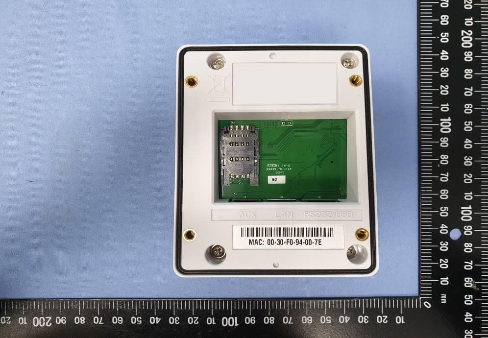
TFJBEZEL8-S
Mar 17, 2021BEZEL8-S Credit card Reader
Equipment Class
DXX - Part 15 Low Power Communication Device Transmitter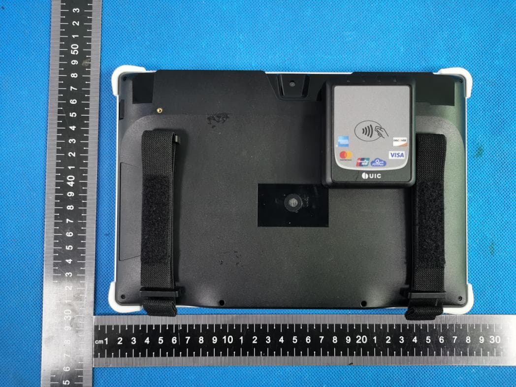
TFJNPOSJUNIOR
Mar 03, 2021Mobile POS Tablet
Equipment Class
NII - Unlicensed National Information Infrastructure TX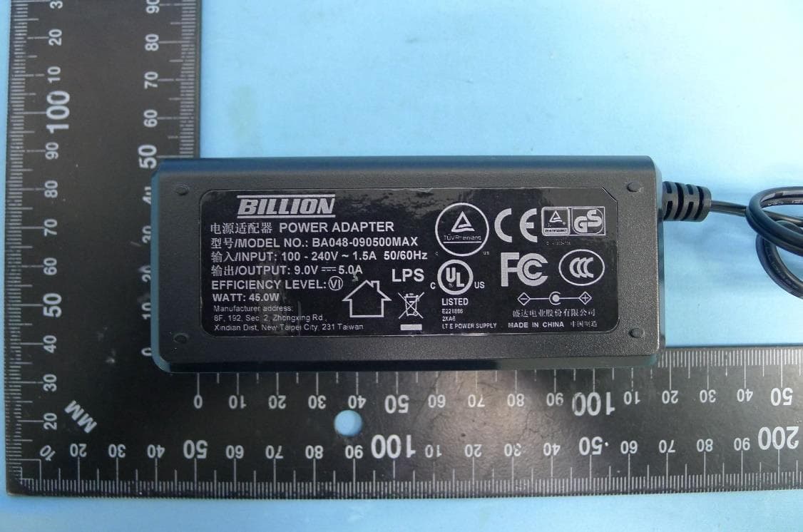
TFJA10-T-ME
Jan 06, 2021Payment Terminal
Equipment Class
PCB - PCS Licensed Transmitter