UA9500444-2216
Summit Semiconductor LLC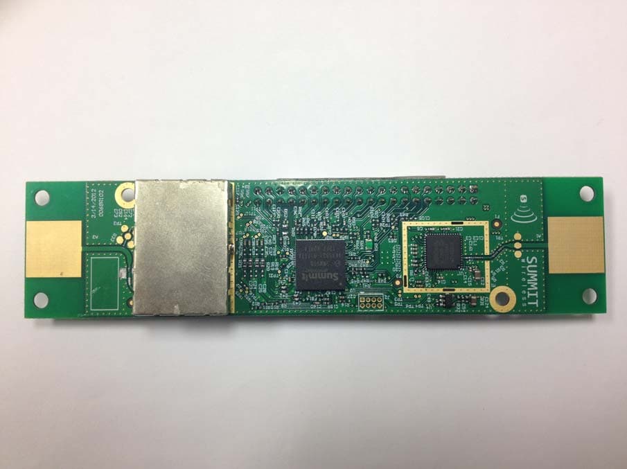
Click to zoom
Application Details
- Equipment Class
- NII - Unlicensed National Information Infrastructure TX
- Date of Grant
- Jan 15, 2013
- Application Purpose
- Original Equipment
- Date of Application
- Aug 26, 2012
- Equipment Note
- 444-2216
- Frequency Range
- 5660.00000000 - 5700.00000000
- Company
- Summit Semiconductor LLC
- Country
- United States
Documents & Files
Document Text
Text extracted from the exhibit documents filed with the FCC. Open a document above to read the original.
Users Manual
SUMMIT SEMICONDUCTOR LLC 22867 NW Bennett Street, Suite 200 Hillsboro, OR 97124 USA Phone: 503 615‐7700 • Fax: 503 615‐4232 http://www.summitsemi.com Glenwood Model 444‐2216 User Manual 1 Table of Contents 2 User Manual Regulatory Statements ............................................................................................. 2 2.1 FCC / IC Identification Numbers .............................................................................................. 2 2.2 FCC/ IC Compliance Statement ............................................................................................... 2 2.3 FCC Changes Warning ............................................................................................................. 2 2.4 FCC / IC Information To The User ........................................................................................... 2 2.5 FCC Labeling ............................................................................................................................ 3 2.6 FCC / IC Antenna usage ........................................................................................................... 3 2.7 Mobile Exposure ...................................................................................................................... 3 2.8 FCC Modular approval configuration control ......................................................................... 3 2.9 FCC / IC Indoor Usage .............................................................................................................. 3 2.10 FCC Interim Solution to DFS band interference with Weather Radar .................................... 4 3 OEM Installation Instructions ......................................................................................................... 4 3.1 Mounting hardware ................................................................................................................ 4 4 OEM Operating Environment ......................................................................................................... 4 5 OEM Operating Instructions ........................................................................................................... 5 SUMMIT SEMICONDUCTOR LLC 22867 NW Bennett Street, Suite 200 Hillsboro, OR 97124 USA Phone: 503 615‐7700 • Fax: 503 615‐4232 http://www.summitsemi.com 2 User Manual Regulatory Statements The United States Federal Communication Commission has established certain rules governing the use of electronic equipment, including the following required guidelines. 2.1 FCC / IC Identification Numbers United States FCC ID UA9500 Industry Canada IC: 9129A‐500 2.2 FCC/ IC Compliance Statement This device complies with Part 15 of the FCC Rules. Operation is subject to the following two conditions: (1) This device may not cause harmful interference, and (2) This device must accept any interference received, including interference that may cause undesired operation. CAUTION: ANY CHANGES OR MODIFICATIONS NOT EXPRESSLY APPROVED BY THE PARTY RESPONSIBLE FOR COMPLIANCE COULD VOID THE USER’S AUTHORITY TO OPERATE THE EQUIPMENT. 2.3 FCC Changes Warning Any changes or modifications not expressly approved by the party responsible for compliance could void the user’s authority to operate the equipment. 2.4 FCC / IC Information to the user Note: This equipment has been tested and found to comply with the limits for a Class B digital device, pursuant to part 15 of the FCC Rules. These limits are designed to provide reasonable protection against harmful interference in a residential installation. This equipment generates, uses and can radiate radio frequency energy and, if not installed and used in accordance with the instructions, may cause harmful interference to radio communications. However, there is no guarantee that interference will not occur in a particular installation. If this equipment does cause harmful interference to radio or television reception, which can be determined by turning the equipment off and on, the user is encouraged to try to correct the interference by one or more of the following measures: —Reorient or relocate the receiving antenna. —Increase the separation between the equipment and receiver. SUMMIT SEMICONDUCTOR LLC 22867 NW Bennett Street, Suite 200 Hillsboro, OR 97124 USA Phone: 503 615‐7700 • Fax: 503 615‐4232 http://www.summitsemi.com —Connect the equipment into an outlet on a circuit different from that to which the receiver is connected. —Consult the dealer or an experienced radio/TV technician for help. Users should also be cautioned to take note that high-power radars are allocated as primary users (meaning they have priority) of the bands 5250-5350 MHz, 5600-5650 MHz, and 5650-5850 MHz and these radars could cause interference and/or damage to WLAN devices. 2.5 FCC Labeling While the FCC user ID is placed on the master device circuit board, compliant labeling shall also be placed on the end product housing exterior. 2.6 FCC / IC Antenna usage Antennas are required to be permanently attached or of non-standard connection method to prevent the end user from altering the installation’s performance. The installer shall be responsible for this. . CAUTION: DO NOT TRY TO REPLACE THE ANTENNAS 2.7 Mobile Exposure The user is cautioned to maintain 20cm (8 inch) spacing from the product to ensure compliance with FCC requirements. 2.8 FCC Modular approval configuration control Control of the end product into which the module will be installed must be maintained such that full compliance of the end product is always ensured. The modular transmitter must comply with any specific rule or operating requirements applicable to the transmitter and the manufacturer must provide adequate instructions along with the module to explain any such requirements. It is the responsibility of the OEM or module level customer to install the master device in accordance with the guidelines of this manual. In order to maintain compliance with…
Text truncated - open the document above for the full version.
Users Manual
SUMMIT SEMICONDUCTOR LLC 22867 NW Bennett Street, Suite 200 Hillsboro, OR 97124 USA Phone: 503 615‐7700 • Fax: 503 615‐4232 http://www.summitsemi.com Glenwood Model 444‐2216 User Manual 1 Table of Contents 2 User Manual Regulatory Statements ............................................................................................. 2 2.1 FCC / IC Identification Numbers .............................................................................................. 2 2.2 FCC/ IC Compliance Statement ............................................................................................... 2 2.3 FCC Changes Warning ............................................................................................................. 2 2.4 FCC / IC Information To The User ........................................................................................... 2 2.5 FCC Labeling ............................................................................................................................ 3 2.6 FCC / IC Antenna usage ........................................................................................................... 3 2.7 Mobile Exposure ...................................................................................................................... 3 2.8 FCC Modular approval configuration control ......................................................................... 3 2.9 FCC / IC Indoor Usage .............................................................................................................. 3 2.10 FCC Interim Solution to DFS band interference with Weather Radar .................................... 4 3 OEM Installation Instructions ......................................................................................................... 4 3.1 Mounting hardware ................................................................................................................ 4 4 OEM Operating Environment ......................................................................................................... 4 5 OEM Operating Instructions ........................................................................................................... 5 6 Compliance with country code requirements.......................................................................................5 SUMMIT SEMICONDUCTOR LLC 22867 NW Bennett Street, Suite 200 Hillsboro, OR 97124 USA Phone: 503 615‐7700 • Fax: 503 615‐4232 http://www.summitsemi.com 2 User Manual Regulatory Statements The United States Federal Communication Commission has established certain rules governing the use of electronic equipment, including the following required guidelines. 2.1 FCC / IC Identification Numbers United States FCC ID UA9500 Industry Canada IC: 9129A‐500 2.2 FCC/ IC Compliance Statement This device complies with Part 15 of the FCC Rules. Operation is subject to the following two conditions: (1) This device may not cause harmful interference, and (2) This device must accept any interference received, including interference that may cause undesired operation. CAUTION: ANY CHANGES OR MODIFICATIONS NOT EXPRESSLY APPROVED BY THE PARTY RESPONSIBLE FOR COMPLIANCE COULD VOID THE USER’S AUTHORITY TO OPERATE THE EQUIPMENT. 2.3 FCC Changes Warning Any changes or modifications not expressly approved by the party responsible for compliance could void the user’s authority to operate the equipment. 2.4 FCC / IC Information to the user Note: This equipment has been tested and found to comply with the limits for a Class B digital device, pursuant to part 15 of the FCC Rules. These limits are designed to provide reasonable protection against harmful interference in a residential installation. This equipment generates, uses and can radiate radio frequency energy and, if not installed and used in accordance with the instructions, may cause harmful interference to radio communications. However, there is no guarantee that interference will not occur in a particular installation. If this equipment does cause harmful interference to radio or television reception, which can be determined by turning the equipment off and on, the user is encouraged to try to correct the interference by one or more of the following measures: —Reorient or relocate the receiving antenna. —Increase the separation between the equipment and receiver. SUMMIT SEMICONDUCTOR LLC 22867 NW Bennett Street, Suite 200 Hillsboro, OR 97124 USA Phone: 503 615‐7700 • Fax: 503 615‐4232 http://www.summitsemi.com —Connect the equipment into an outlet on a circuit different from that to which the receiver is connected. —Consult the dealer or an experienced radio/TV technician for help. Users should also be cautioned to take note that high-power radars are allocated as primary users (meaning they have priority) of the bands 5250-5350 MHz, 5600-5650 MHz, and 5650-5850 MHz and these radars could cause interference and/or damage to WLAN devices. 2.5 FCC Labeling While the FCC user ID is placed on the master device circuit board, compliant labeling shall also be placed on the end product housing exterior. 2.6 FCC / IC Antenna usage Antennas are required to be permanently attached or of non-standard connection method to prevent the end user from altering the installation’s performance. The installer shall be responsible for this. . CAUTION: DO NOT TRY TO REPLACE THE ANTENNAS 2.7 Mobile Exposure The user is cautioned to maintain 20cm (8 inch) spacing from the product to ensure compliance with FCC requirements. 2.8 FCC Modular approval configuration control Control of the end product into which the module will be installed must be maintained such that full compliance of the end product is always ensured. The modular transmitter must comply with any specific rule or operating requirements applicable to the transmitter and the manufacturer must provide adequate instructions along with the module to explain any such requirements. It is the responsibility of the OEM or modul…
Text truncated - open the document above for the full version.
Attestation Statements
SUMMIT SEMICONDUCTOR LLC 22867 NW Bennett Street, Suite 200 Hillsboro, OR 97124 USA Phone: 503 615-7700 • Fax: 503 615-4232 http://www.summitsemi.com 27 November, 2012 Federal Communications Commission Authorization and Evaluation Branch 7435 Oakland Mills Road Columbia, MD 21046 Dear Application Examiner: This letter is in response to an email received on 11-07-2012 from FCC’s Office of Engineering and Technology requesting us to demonstrate how we would comply with the software configuration control and county code requirements of KDB 594280. I have illustrated an example of the step by step process that Summit Semiconductor LLC will follow to comply with the requirements in KDB 594280. • The digital wireless master module (Model No.: 444-2216, FCC ID: UA9500) is typically manufactured by a contract manufacturer. (CM) • Summit will provide only one version of flash memory image to the contract manufacturer. The flash memory image, among many other things includes the country code selection field. • The default country code selection in the flash memory image is set to USA and the CMs will not have access to this field. • The modules are then shipped from our contract manufacturer to our ODMs. • Our ODMs typically will need to sell their product containing our wireless master module in different countries and also would require some control over the audio configuration fields depending on the end product the wireless module is integrated into. • At this point in time, our ODMs will request Summit Semiconductor to provide them with a software program for a particular country that will allow them the access over the audio configuration fields. • Summit will provide the software program with the country code already hard coded to a particular country that the ODM has requested so that our ODMs can change only audio related configuration. • Once the ODM completes the audio configuration changes and runs the software program, the country code is set automatically without ODM input. The program then verifies the settings for the ODM guarantying the correct application of the country code. • The software program provided by Summit is country dependent. Our ODMs will have to use different software programs for different countries. This process will ensure that Summit Semiconductor has direct control over the country code selection field and the third parties including the end users and professional installers do not have access to it. It also ensures that the third parties cannot operate the device out of compliance of the technical rules under which the device has been certified. Summit will also make it a requirement that ODMs sign an attestation statement ensuring that a module programmed to a specific country code will only be used in products shipped to that country. Sincerely, Ponnappa Pasura Sr. RF Engineer
Cover Letter(s)
SUMMIT SEMICONDUCTOR LLC 22867 NW Bennett Street, Suite 200 Hillsboro, OR 97124 USA Phone: 503 615-7700 • Fax: 503 615-4232 http://www.summitsemi.com Request for Confidentiality August 10, 2012 Federal Communications Commission Authorization and Evaluation Branch 7435 Oakland Mills Road Columbia, MD 21046 Re: Summit Semiconductor Certification Application FCC ID: UA9500 To Whom It May Concern: A portion of the data contained in this application is to be considered a trade secret and not to be made routinely available to the public. If such information were to be made public, it might be used to the disadvantage of Summit Semiconductor LLC (the applicant) in the market place. Therefore, pursuant to 47 CFR 0.459 and 47 CFR 0.457(d) of the FCC Rules, we request that the information listed below be withheld from public inspection: Schematics Frequency Block Diagrams Operational Description Thank you for your attention to this matter. Sincerely, James Svoboda Engineering Manager
Cover Letter(s)
SUMMIT SEMICONDUCTOR LLC 22867 NW Bennett Street, Suite 200 Hillsboro, OR 97124 USA Phone: 503 615-7700 • Fax: 503 615-4232 http://www.summitsemi.com 20 November, 2012 Federal Communications Commission Authorization and Evaluation Branch 7435 Oakland Mills Road Columbia, MD 21046 Dear Application Examiner: Summit Semiconductor LLC has designed and built a digital wireless master module that operates in the UNII band including the DFS frequencies. Summit Semiconductor requests FCC Equipment and Authorization branch to grant an original certification as a “single-modular approval” for our wireless master module, Model No.: 444-2216, FCC ID: UA9500. The 444-2216 wireless master module is a turnkey solution that enables customers to start volume production of high performance digital wireless audio source devices. The 444-2216 is designed to be integrated into an audio source device such as AVRs, DVD players, TVs, gaming consoles, set top boxes and wireless hubs. It is an IEEE 802.11a compliant radio operating in UNII band and operates in accordance with the master mode as stated in the FCC 06-96. The 444-2216 wireless master module was tested at NWEMC’s Oregon facility for rule parts 15.247 and 15.407 and at UL-CCS, California facility for rule part 15.407. The device was tested for all the requirements necessary to certify it as a limited modular, DFS capable, and 21 channel transmitter. The test set up photos and the technical test report has all the details about the performance and results of the device. The device is subject to verification and not DoC because it is not a PC peripheral Please address any correspondence regarding this filing to my attention at the following address. Summit Semiconductor LLC 22867 NW Bennett St., Suite 200 Hillsboro, OR 97124 Ph: 503 615-7734 Sincerely, James Svoboda Engineering Manager
Cover Letter(s)
SUMMIT SEMICONDUCTOR LLC 22867 NW Bennett Street, Suite 200 Hillsboro, OR 97124 USA Phone: 503 615-7700 • Fax: 503 615-4232 http://www.summitsemi.com 20 November, 2012 Federal Communications Commission Authorization and Evaluation Branch 7435 Oakland Mills Road Columbia, MD 21046 Subject: Request for unlicensed Limited Modular Transmitter Approval. Dear Application Examiner: Summit Semiconductor LLC hereby requests FCC Equipment Authorization and Evaluation branch to approve Summit Semiconductor LLC Model 444-2216, digital wireless audio master device, FCC ID-UA9500, as a “single-modular approval” for 21 channel DFS enabled transmitter. This letter addresses the information required by points one through eight of 47 CFR 15.212. 1. “The modular transmitter must have its own RF shielding .” The transmitter radio section of the module is enclosed within a RF shield. The RF shield is solder mounted to the exposed grounding of the circuit board. The point of contact between the shield and the board has multiple ground contacts. The internal photos exhibit has pictures of the wireless master device with and without the shield. The shield suppresses spurious radiations as per FCC requirements. 2. “The modular transmitter must have buffered modulation/data inputs.” The 444-2216 has buffered data inputs that pass through an embedded processor. RF modulation controls are generated on board. Firmware will also not allow the end user to access RF modulation / data rate control settings of the RF circuitry. No change in input data or control signal can affect the RF data rate or type. This method insures compliance with Part 15 requirements under conditions of excessive data rates or over modulation. 3. “The modular transmitter must have its own power supply regulation.” The 444-2216 digital wireless master device receives power from an external +3.3 VDC and external +1.2 VDC supply on the customer’s host controller board. The +3.3 VDC supply sources some circuitry directly and is also regulated to +2.8 VDC. The +1.2 VDC supply sources circuitry directly. In order to comply with the requirement that all voltages be regulated, we have included an over voltage detection circuit which ceases RF transmission when the input voltages exceed their +10% threshold, either independently or together. 4. “The modular transmitter antenna must comply with the antenna and transmission system requirements of section 15.203, and 15.204(c).” The modular device complies with all FCC antenna requirements. The 444-2216 digital wireless master device is designed in such a way that the antenna is integrated with the modular device. As per the FCC 15.203 requirement, this can be considered as permanently attached and doesn’t give the user any option to replace it. A list of usable antennas is not provided since the user manual clearly instructs the user that the modular device is compatible with only the integrated antenna. The antenna report also provides a description as to how the modular device complies with the de facto EIRP limit. 5. “The modular transmitter must be tested in a stand-alone configuration.” As described in the technical report exhibit and the test set up photos of the test report included in the filing for FCC equipment authorization, the 444-2216 digital wireless master device module was tested as a standalone device. The device is designed with an industry standard multi pin connector and was tested in typical configuration which is greater than 10 cm in length from the host device. 6. “The modular transmitter must be equipped with either a permanently affixed label or must be capable of electronically displaying the FCC identification number.” A FCC ID and model number is labeled on every modular device. FCC ID label and location exhibit has a photograph which shows the exact location of the label. Since the FCC ID number will not be visible when the module is installed inside the host audio source, another label with the same FCC ID will be applied to the exterior of the host/master enclosure. 7. “The modular transmitter must comply with any specific rule or operating requirements applicable to the transmitter and the manufacturer must provide adequate instructions along with the module to explain any such requirements.” The EUT complies with all specific rules such as modulation scheme, modulation type, bandwidth, antenna requirements, power supply regulation, and suppression of spurious emissions and so on. A detailed user manual is provided with every EUT which instructs the user to maintain compliance as per the requirements of the Commission. The manual also cautions the user not to make any changes or modifications not approved by the party responsible for compliance. Please see the operating description exhibit for further details to understand how the EUT complies with specific rules and operating requirements as per FCC. 8. “The modular transmitter must comply with any applicable RF exposure requirements in its final configuration.” The EUT is compliant with all applicable RF exposure requirements and EUT is operated in a manner that ensures the public is not exposed to radio frequency in excess of Federal Communication Commission’s guidelines. Please see the RF exposure exhibit. Best Regards James Svoboda Engineering Manager
External Photos
SUMMIT SEMICONDUCTOR LLC SUMMIT SWM 908 MASTER MODULE Model No. 444-2216 22867 NW Bennett St., Suite 200 www.summitsemi.com Hillsboro, OR 97124 TEL (503) 615 7734 FAX: (503) 615 4432 © 2010 Summit Semiconductor LLC SUMMIT SEMICONDUCTOR LLC Model No.: 444-2216 FCC ID: UA9500 EXTERNAL PHOTOS SUMMIT SEMICONDUCTOR LLC SUMMIT SWM 908 MASTER MODULE Model No. 444-2216 2 of 3 22867 NW Bennett St., Suite 200 www.summitsemi.com FRONT SIDE WITH RF SHIELDING Hillsboro, OR 97124 TEL (503) 615 7734 FAX: (503) 615 4432 © 2010 Summit Semiconductor LLC SUMMIT SEMICONDUCTOR LLC SUMMIT SWM 908 MASTER MODULE Model No. 444-2216 3 of 3 22867 NW Bennett St., Suite 200 www.summitsemi.com BACK SIDE Hillsboro, OR 97124 TEL (503) 615 7734 FAX: (503) 615 4432 © 2010 Summit Semiconductor LLC
ID Label/Location Info
SUMMIT SEMICONDUCTOR LLC SUMMIT SWM 908 MASTER MODULE Model No. 444-2216 22867 NW Bennett St., Suite 200 www.summitsemi.com Hillsboro, OR 97124 TEL (503) 615 7734 FAX: (503) 615 4432 © 2010 Summit Semiconductor LLC SUMMIT SEMICONDUCTOR LLC Model No.: 444-2216 FCC ID: UA9500 FCC ID and LOCATION SUMMIT SEMICONDUCTOR LLC SUMMIT SWM 908 MASTER MODULE Model No. 444-2216 2 of 2 22867 NW Bennett St., Suite 200 www.summitsemi.com FCC ID AND LOCATION Hillsboro, OR 97124 TEL (503) 615 7734 FAX: (503) 615 4432 © 2010 Summit Semiconductor LLC
ID Label/Location Info
The FCC ID and IC will appear on the host device as shown in the example below. Contains: FCC ID: UA9500 IC: 9129A-500
Internal Photos
SUMMIT SEMICONDUCTOR LLC SUMMIT SWM 908 MASTER MODULE Model No. 444-2216 22867 NW Bennett St., Suite 200 www.summitsemi.com Hillsboro, OR 97124 TEL (503) 615 7734 FAX: (503) 615 4432 © 2010 Summit Semiconductor LLC SUMMIT SEMICONDUCTOR LLC Model No.: 444-2216 FCC ID: UA9500 INTERNAL PHOTOS SUMMIT SEMICONDUCTOR LLC SUMMIT SWM 908 MASTER MODULE Model No. 444-2216 2 of 4 22867 NW Bennett St., Suite 200 www.summitsemi.com FRONT SIDE WITH RF SHIELDING Hillsboro, OR 97124 TEL (503) 615 7734 FAX: (503) 615 4432 © 2010 Summit Semiconductor LLC SUMMIT SEMICONDUCTOR LLC SUMMIT SWM 908 MASTER MODULE Model No. 444-2216 3 of 4 22867 NW Bennett St., Suite 200 www.summitsemi.com BACK SIDE Hillsboro, OR 97124 TEL (503) 615 7734 FAX: (503) 615 4432 © 2010 Summit Semiconductor LLC SUMMIT SEMICONDUCTOR LLC SUMMIT SWM 908 MASTER MODULE Model No. 444-2216 4 of 4 22867 NW Bennett St., Suite 200 www.summitsemi.com FRONT SIDE WITHOUT RF SHIELDING Hillsboro, OR 97124 TEL (503) 615 7734 FAX: (503) 615 4432 © 2010 Summit Semiconductor LLC
RF Exposure Info
Summit Semiconductor Model# 444-2216 (Glenwood) Report No. FOCU0127.4 FCC 2.1091: Maximum Permissible Exposure Level Report Prepared By Northwest EMC Inc. NORTHWEST EMC – (888) 364-2378 – www.nwemc.com California – Minnesota – Oregon – New York – Washington 22975 NW Evergreen Parkway Suite 400 Hillsboro, Oregon 97124 Certificate of Evaluation Date of Evaluation August 10, 2012 Summit Semiconductor Model: 444-2216 (Glenwood) Emissions Description of Evaluation Specification Evaluation Method Pass/Fail Maximum Permissible Exposure FCC 2.1091:2012 OET Bulletin 65, Supplement C Ed 01-01 Pass Approved By: Don Facteau, IS Manager NVLAP Lab Code: 200630-0 This report must not be used to claim product certification, approval, or endorsement by NVLAP, NIST, or any agency of the federal government of the United States of America. Product compliance is the responsibility of the client, therefore the tests and equipment modes of operation represented in this report were agreed upon by the client, prior to testing. This Report may only be duplicated in its entirety. The results of this test pertain only to the sample(s) tested. The specific description is noted in each of the individual sections of the test report supporting this certificate of test. Report No. FOCU0127.42/9 REV 2012.05.24 REVISION HISTORY Revision Number Description Date Page Number 00 None Report No. FOCU0127.43/9 REV 2012.05.24 ACCREDITATIONS AND AUTHORIZATIONS United States FCC - Designated by the FCC as a Telecommunications Certification Body (TCB). Certification chambers, Open Area Test Sites, and conducted measurement facilities are listed with the FCC. A2LA - Accredited by A2LA to ISO / IEC Guide 65 as a product certifier. This allows Northwest EMC to certify transmitters to FCC and IC specifications. NVLAP - Each laboratory is accredited by NVLAP to ISO 17025 Canada IC - Recognized by Industry Canada as a Certification Body (CB). Certification chambers and Open Area Test Sites are filed with IC. European Union European Commission – Validated by the European Commission as a Conformity Assessment Body (CAB) under the EMC directive and as a Notified Body under the R&TTE Directive. Australia/New Zealand ACMA - Recognized by ACMA as a CAB for the acceptance of test data. Korea KCC / RRA - Recognized by KCC’s RRA as a CAB for the acceptance of test data. Japan VCCI - Associate Member of the VCCI. Conducted and radiated measurement facilities are registered. Taiwan BSMI – Recognized by BSMI as a CAB for the acceptance of test data. NCC - Recognized by NCC as a CAB for the acceptance of test data. Singapore IDA – Recognized by IDA as a CAB for the acceptance of test data. Hong Kong OFTA – Recognized by OFTA as a CAB for the acceptance of test data. Vietnam MIC – Recognized by MIC as a CAB for the acceptance of test data. Russia GOST – Accredited by Certinform VNIINMASH, CERTINFO, SAMTES, and Federal CHEC to perform EMC and Hygienic testing for Information Technology products to GOST standards. SCOPE For details on the Scopes of our Accreditations, please visit: http://www.nwemc.com/accreditations/ Report No. FOCU0127.44/9 REV 2012.05.24 LOCATIONS Oregon Labs EV01-EV12 22975 NW Evergreen Pkwy, #400 Hillsboro, OR 97124 (503) 844-4066 California Labs OC01-OC13 41 Tesla Irvine, CA 92618 (949) 861-8918 New York Labs WA01-WA04 4939 Jordan Rd. Elbridge, NY 13060 (315) 685-0796 Minnesota Labs MN01-MN08 9349 W Broadway Ave. Brooklyn Park, MN 55445 (763) 425-2281 Washington Labs SU01-SU07 14128 339 th Ave. SE Sultan, WA 98294 (360) 793-8675 VCCI A-0108 A-0029 A-0109 A-0110 Industry Canada 2834D-1, 2834D-2 2834B-1, 2834B-2, 2834B-3 2834E-1 2834C-1 Report No. FOCU0127.45/9 Product Description Revision 09/01/11 Client and Equipment Under Test (EUT) Information Company Name: Summit Semiconductor Address: 22867 NW Bennett St, Suite 200 City, State, Zip: Hillsboro, OR 97124 Test Requested By: Ponnappa Pasura Model: Model# 444-2216 (Glenwood) Date of Evaluation: August 10, 2012 Information Provided by the Party Requesting the Test Functional Description of the EUT (Equipment Under Test): UNII radio module operating in the 5.2, 5.3, 5.6 and 5.8 GHz bands Objective: To demonstrate compliance with FCC requirements for RF exposure for 2.1091 mobile devices Report No. FOCU0127.46/9 WD.12.29.11 Maximum Permissible Exposure (MPE) OVERVIEW Human exposure to RF emissions from mobile devices (47 CFR §2.1091) may be evaluated based on the MPE limits adopted by the FCC for electric and magnetic field strength and/or …
Text truncated - open the document above for the full version.
Contact Information
Applicant
Ken N Boehlke(Engineering Manager)
Test Firm
Northwest EMC, Inc.Greg Kiemel
Technical Specifications
| # | Rule Parts | Frequency Range | Power Output |
|---|---|---|---|
| 4 | 15E | 5.66 GHz - 5.70 GHz | 35.00 mW |
Other Applications from Summit Semiconductor LLC
UA9800
Oct 28, 2014444-2251
Equipment Class
NII - Unlicensed National Information Infrastructure TX
UA9700
Jul 08, 2013444-2225
Equipment Class
NII - Unlicensed National Information Infrastructure TX
UA9600
Jul 08, 2013444-2224
Equipment Class
DTS - Digital Transmission System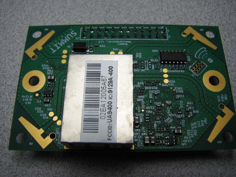
UA9400
Nov 29, 2011444-2213
Equipment Class
NII - Unlicensed National Information Infrastructure TX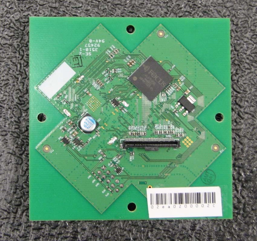
UA9300
Dec 12, 2010444-2196H
Equipment Class
NII - Unlicensed National Information Infrastructure TX