UAYK402IoT Development Kit
Marvell Semiconductor, Inc.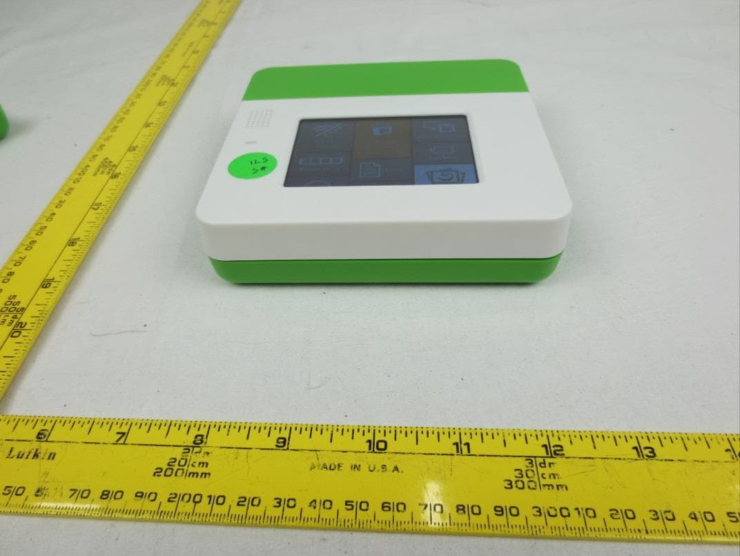
Click to zoom
Application Details
- Equipment Class
- NII - Unlicensed National Information Infrastructure TX
- Date of Grant
- Dec 02, 2015
- Application Purpose
- Original Equipment
- Date of Application
- Dec 02, 2015
- Equipment Note
- IoT Development Kit
- Frequency Range
- 5210.00000000 - 5210.00000000
- Company
- Marvell Semiconductor, Inc.
- Country
- United States
Documents & Files
Document Text
Text extracted from the exhibit documents filed with the FCC. Open a document above to read the original.
Users Manual
User Manual Model K4-02 Front Pins Files Battery Logs File Sharing Settings My Device office Wi-Fi 10.0.1.51 Table of Contents 1. Important Information 2. Kinoma Create hardware 4. First Run 7. Powering on/o 8. Charging internal battery 9. Network Connection: Wi-Fi 10. Settings 14. On-board applications 17. Setting up a bootable SD card 18. Connecting to PC 19. Using Hardware Pins (Front Pins) 20. Using Hardware Pins (Rear Pins) 21. Kinoma Create Stand 22. FCC Statement Important Information about Kinoma Create The most important thing to know is that Kinoma Create is primarily a 3.3-volt system. If you’re new to 3.3v systems or to hardware in general, this means that (unlike with an Arduino or some other boards), you can only send up to 3.3 volts into any input pin on the device without doing damage to the pin. Download Kinoma Studio. You can try out your own applications in our desktop simulator, build apps for iOS and Android, or run any of our samples (included with Kinoma Studio) on your Kinoma Create. Our team is ready to support you as you work with your Kinoma Create. The best way to get answers to your questions is to post on the Kinoma Forum (http://forum.kinoma.com/). We will post there, and email a second time, once the hardware documentation is available. We want you all to successfully bring your product concepts to life, and we’ll be here to help you along the way. Enjoy your Kinoma Create! 1 Cable port for routing cables out from rear pins 16 pins configurable for: • 5V or 3.3V power • Ground • Digital input/output • Analog input • I2C • PWM • Serial Removable sensor cover Speaker microSD slot USB 2.0 including USB On-The-Go Microphone Mini USB serial console port Color screen Capacitive touch screen Kinoma Create Front 2 Removable access panel 50 pins for: • 3.3V power • Ground • Digital input/output • Analog input • I2C • PWM • Serial Stand Dowels Stand Holes Reset Kinoma Create Back 3 Kinoma Create First Run 4 1 2 Begin charging device with supplied charger. (Note: Kinoma Create uses special charging circuitry and requires a sensing charger to correctly charge the battery. Only use the provided charger, since other chargers may not charge the battery). Remove back cover and pull out battery contact shield. 3 4 Press the power button on the back of Kinoma Create. Kinoma Create typically takes 35 seconds to boot up. Use the Wi-Fi app to add your Kinoma Create to your network.. Kinoma Create First Run 5 5 Set the time zone for your device. Kinoma Create First Run 6 Power On/O Press to start If powered up, long press shuts down If powered up, and a short press, device enters hibernate mode. If powered up, and in hibernate mode, a short press wakes up Reset device button. Use paper clip or similar to reach reset button and perform a hard reset. This screen shows during boot up. Kinoma Create typically takes 35 seconds to start. 7 Charging internal battery Kinoma Create uses special charging circuitry and requires a sensing charger to correctly charge the battery. Only use the provided charger, since other char- gers may not charge the battery 8 Network Connection: Wi-Fi Clicking the “Select network” button displays a list of available networks. Select a network and enter password if necessary. Kinoma Create remem- bers the last configured Wi-Fi network. A er connecting to a network the device IP address is shown on the Wi-Fi tile. 9 Settings The Settings app on Kinoma Create allows for setting attributes, updating device and viewing device information. If updates are available an UPDATE notification will appear. Tap to update. 10 Settings 11 Name: Set Device name if needed. This is the name that this Kinoma Create will use for network connections, including debugging in the Kinoma Studio IDE. Time zone: It is important to set the local timezone for apps that use time and date based APIs. The optional day light savings check box needs to be manually update to match local conditions. Startup App: For testing Kinoma Create can be set to launch into a specific app. The default is the Kinoma Create Launcher app. 12 Settings Quit Gesture: Allows selection of quit gesture Delete Apps: Allows removal of apps that have been installed on Kinoma Create. Note: Built-in apps, such as Wi-Fi and Settings cannot be deleted. Debugging: Kinoma Create can be set to allow debugging over Wi-Fi and require a password to debug. Kinoma So ware: Shows the current version number and Updates if available. 13 Settings Firmware (OS): Shows the current firmware version number and Updates if available. Setup SD card: Format and partition an SD to become a bootable file system Clear Caches: Allows clearing of Kinoma Studio App, Cookie and HTTP caches MAC Address: Shows the MAC address of this Kinoma Create. The MAC address is the unique id of the device. On Board Apps 14 Battery: Shows current charge status on the tile and chargingand usage history in the app view. File Sharing App: Allows mouning your Kinoma Create on your PC (Windows and Mac). File Sharing implements the WebDAV protocol 15 On Board Apps Front Pins: The 16 front facing pins can be targeted by the Front Pins app to support Digital, Analog In, and I2C connections. Power can be supplied at 3.3 or 5 volts. Input pins will handle up to 3.3v. Files: Files app provides simple view and management functionality for files on Kinoma Create. It can display PNG and JPEG images, MPEG-4 files, and the first 8KB of text based files. Individual files can be deleted. 16 On Board Apps Logs: Presents information about the operation of Kinoma Create. Kinoma Create logs PinMux settings, Settings, system events and Wi-Fi configurations. Developers can add new logs or data to existing logs. Samples: Shows current contents from the Kinoma GitHub Samples repository. Select samples to download and view on the device. Select View Source to view the JavaScript source and other project assets. Setting up a bootable SD card 17 Install an SD card and you can set it u…
Text truncated - open the document above for the full version.
Attestation Statements
Confidentiality Requested @2015 MARVELL CONFIDENTIAL SOFTWARE SECURITY DECLARATION FOR U‐NII DEVICES Kinoma Create December 2, 2015 This document is prepared for the Marvell Kinoma Create device, and the document responds to the questions posed in KDB 594280 D02 U‐NII Device Security v01r03 (Nov. 12, 2015). Kinoma Create is a prototyping device for developing internet connected embedded devices. The device is powered by an efficient ARM CPU with Wi‐Fi connectivity (802.11ac 1x1), and has a capacitive color touch screen and 66 I/O pins. The following terminologies are used in this declaration: 1. Host software/firmware: these include host operating system and device driver running on host CPU. 2. Wi‐Fi firmware: this refers to the embedded Wi‐ Fi firmware running on the Wi‐Fi connectivity chip. This is specialized software that configures and controls the underlying Wi‐Fi hardware, including RF parameter settings. The following is a summary of security measures taken to ensure FCC compliance: 1. The FCC Region Code is factory‐set in OTP (one‐time ‐programmable memory) on the device and is fixed in Wi‐Fi firmware. 2. The RF parameter settings are restricted in the Wi‐Fi firmware based on Region Code. For FCC region, the RF parameters are restricted to be compliant with FCC rules, for both client and master modes. 3. Kinoma Create is only configured in client mode by default and through the user interface. The user interface does not support access point (master) mode configuration. 4. Kinoma Create uses the same antenna for all modes of operations. 5. Kinoma Create software/firmware updates are retrieved using the HTTPS protocol for secure file transfer and a private certificate for authentication. 6. A non‐standard CRC32 based integrity check is built into the Wi‐Fi firmware loading procedure to ensure that the source has not been tampered with. 7. An OTP flag is used to invalidate previously released Wi‐Fi firmware and make the device inoperable. Confidentiality Requested @2015 MARVELL CONFIDENTIAL SOFTWARESECURITYDESCRIPTION General Description 1. Describe how any software/firmwareupdatesforelementsthat can affect thedevice’s RF parameters will be obtained, downloaded, validated and installed. For software that is accessed through manufacturer’s website or device’s management system, describe the different levels of security as appropriate. [MRVL] The user interface of Kinoma Create provides a visual indication to the user when a software update is available. All updates are initiated by the user, there are no automatic updates. Updates are retrieved from a Marvell managed web server hosted on Amazon Cloud Services. The updates are retrieved using the HTTPS protocol for secure file transfer and a private certificate for authentication. The RF parameter settings are restricted in the Wi‐Fi firmware. Only compiled Wi‐Fi firmware binary code is available for download, not source code. Please refer to questions 2 and 3 for RF parameters compliance and additional Wi‐Fi firmware security protection. 2. Describe the RF parametersthataremodified byanysoftware/firmware withoutany hardware changes. Are these parameters in some way limited such that any other software/firmware changes will not allow the device to exceed the authorized RF characteristics? [MRVL] The Wi‐Fi firmware provides an API which can be called to configure the Wi‐Fi band, channel number, bandwidth, and Tx power level. The allowable settings are restricted to Region Code of the device. The Kinoma Create devices have factory‐set FCC Region Code in OTP (one‐time programmable memory) and the RF parameter settings are restricted to be compliant with FCC rules in the Wi‐Fi firmware. Confidentiality Requested @2015 MARVELL CONFIDENTIAL 3. Describe in detail the authentication protocolsthatarein place to ensure thatthe source of the RF‐related software/firmware is valid. Describe in detail how the RF‐ related software is protected against modification. [MRVL] The R F‐related software/firmware is the Wi‐Fi firmware. The Wi‐Fi connectivity chip is a specialized ASIC (application‐specific‐integrated‐circuit) which contains specialized hardware and software to optimize performance. The radio is integrated into the Wi‐Fi chip. For the device to operate properly, thousands of registers need to be programmed in the correct sequence by the Wi‐Fi firmware. All design documents are Marvell trade secrets and are well controlled within the company. For customers of Kinoma Create, datasheet and register information are not shared. Only compiled Wi‐Fi firmware binary code is available for download, not source code. A CRC32 based integrity check is built into the Wi‐Fi firmware loading procedure to ensure that the source has not been tampered with. The CRC32 is calculated across each downloaded firmware section. This CRC check is a non‐standard procedure and not shared with customers, so it is not easily reproducible by developers unfamiliar with the internal design of the Wi‐Fi chip. A version flag is programmed into the OTP of the Wi‐Fi chip. This flag ensures that older versions of the Wi‐Fi firmware, which did not respect the Region Code, will not be recognized by the Wi‐Fi chip and therefore will not run. This prevents an attacker from rolling back to an older version of the Wi‐Fi firmware which did not limit RF parameters based on the Region Code. To date, there is no known case of our Wi‐Fi firmware being modified or replaced. Any other attempts, i.e. through device driver, to operate outside the authorized range will be disqualified by Wi‐Fi firmware and will not take effect on the Wi‐Fi radio. 4. Describe in detail any encryption methods used to support the use of legitimate RF‐ related software/firmware. [MRVL] The Wi‐Fi firmware is not encrypted. As described in the response to Question 3, the nature of the device and the buil t‐in firmware download and verification process make it difficult for a 3 rd party to create a new Wi‐Fi firmwar…
Text truncated - open the document above for the full version.
Block Diagram
55 44 33 22 11 D D C C B B A A This Design is given "AS IS" without warranty of an y kind, either expressed or implied. TitleSize Document Number Rev Date: Sheet of Marvell Technology Ltd Kinoma Create 5.1 Main Board Custom 1 19 Tuesday, May 19, 2015 TitleSize Document Number Rev Date: Sheet of Marvell Technology Ltd Kinoma Create 5.1 Main Board Custom 1 19 Tuesday, May 19, 2015 TitleSize Document Number Rev Date: Sheet of Marvell Technology Ltd Kinoma Create 5.1 Main Board Custom 1 19 Tuesday, May 19, 2015
External Photos
Marvell Semiconductor, Inc. FCC ID: UAYK402; IC: 6549A-K402 Report Number: R1506088-407 Page 78 of 83 FCC Part 15.407/IC RSS-247 Test Report 14 Exhibit C – EUT Photographs 1.7 EUT – Front View 1.8 EUT – Rear View Marvell Semiconductor, Inc. FCC ID: UAYK402; IC: 6549A-K402 Report Number: R1506088-407 Page 79 of 83 FCC Part 15.407/IC RSS-247 Test Report 1.9 EUT – Right Side View 1.10 EUT – Left Side View Marvell Semiconductor, Inc. FCC ID: UAYK402; IC: 6549A-K402 Report Number: R1506088-407 Page 80 of 83 FCC Part 15.407/IC RSS-247 Test Report 1.11 EUT – Top View 1.12 EUT – Bottom View
Internal Photos
Marvell Semiconductor, Inc. FCC ID: UAYK402; IC: 6549A-K402 Report Number: R1506088-407 Page 81 of 83 FCC Part 15.407/IC RSS-247 Test Report 1.13 EUT – Open Case View Top 1.14 EUT – Main Board Top View Marvell Semiconductor, Inc. FCC ID: UAYK402; IC: 6549A-K402 Report Number: R1506088-407 Page 82 of 83 FCC Part 15.407/IC RSS-247 Test Report 1.15 EUT – Main Board Bottom View 1.16 EUT – Battery Board Top View Marvell Semiconductor, Inc. FCC ID: UAYK402; IC: 6549A-K402 Report Number: R1506088-407 Page 83 of 83 FCC Part 15.407/IC RSS-247 Test Report 1.17 EUT – Battery Board Bottom View 1.18 EUT – AC/DC Adapter --- END OF REPORT ---
Operational Description
Kinoma Create Operational Description Kinoma Create is a prototyping device for developing internet connected embedded devices. It is powered by an efficient ARM CPU with Wi‑Fi connectivity, a capacitive color touch screen, and 66 I/O pins. Start Kinoma Create by pressing the white power button on the back. The Kinoma logo appears immediately indicating the device is booting. The logo will display for approximately 45 seconds (please check). After boot up completes the screen displays the on-board applications for configuring the Kinoma Create. Wi-Fi Tile displays the currently connected Wi-Fi network, if any, and device’s IP address. Clicking the “Select network” button displays a list of available networks. Select a network and enter password if necessary. Kinoma Create remembers the last configured Wi-Fi network. Settings Tile shows Kinoma Create name, along with the time and date. The time and date are only displayed after Kinoma Create successfully connected to the Internet. Name: Set Device name if needed. This is the name that this Kinoma Create will use for network connections, including debugging in the Kinoma Studio IDE. Timezone: It is important to set the local timezone for apps that use time and date based API's. The optional day light savings check box needs to be manually update to match local conditions. Startup App: For testing Kinoma Create can be set to launch into a specific app. The default is the Kinoma Create Launcher app. Delete Apps: Allows removal of apps that have been installed on Kinoma Create. Note: built-in apps, such as Wi-Fi and Settings cannot be deleted. Debugging: Kinoma Create can be set to Allow debugging over W-Fi and require a password to debug. Version: Shows the current version number and Updates if available. Clear Caches: Allows clearing of Kinoma Studio App, Cookie and HTTP caches Reset SD card: Format and partition an SD to become a bootable file system MAC Address: Shows the MAC Address of this Kinoma Create. The MAC address is the unique id of the device. Battery Tile shows current battery charging status and percentage of charge Graph shows battery percentage over the last 120 minutes Front Pin Muxing Allows user to select either right or left front headers and assign pin functionality to the individual pins. Each header can have separate voltages. Mux settings are saved across device restarts Logs Logs contains information about the operation of Kinoma Create. Kinoma Create logs PinMux settings, Settings, System events, Wi-Fi configurations. Developers can add new logs or data to existing logs. Files Files app provides simple view and management functionality for files on Kinoma Create. It can display PNG and JPEG images, MPEG-4 files, and the first 8KB of text based files. Individual files can be deleted. Samples Samples app shows current contents from the Kinoma GitHub Samples repository. Select samples to download and view on the device. Select View Source to view the JavaScript source and other project assets.
RF Exposure Info
Marvell Semiconductor, Inc. FCC ID: UAYK402; IC: 6549A-K402 Report Number: R1506088-407 Page 9 of 83 FCC Part 15.407/IC RSS-247 Test Report 4 FCC §2.1091, §15.407(f) & IC RSS-102 - RF Exposure 4.1 Applicable Standard According to FCC §15.407(f) and §1.1307(b)(1), systems operating under the provisions of this section shall be operated in a manner that ensures that the public is not exposed to radio frequency energy level in excess of the Commission’s guidelines. Limits for General Population/Uncontrolled Exposure Frequency Range (MHz) Electric Field Strength (V/m) Magnetic Field Strength (A/m) Power Density (mW/cm 2 ) Averaging Time (minutes) Limits for General Population/Uncontrolled Exposure 0.3-1.34 614 1.63 * (100) 30 1.34-30 824/f 2.19/f * (180/f 2 ) 30 30-300 27.5 0.073 0.2 30 300-1500 / / f/1500 30 1500-100,000 / / 1.0 30 f = frequency in MHz * = Plane-wave equivalent power density According to IC RSS-102 Issue 5 section 4, RF limits used for general public will be applied to the EUT. Marvell Semiconductor, Inc. FCC ID: UAYK402; IC: 6549A-K402 Report Number: R1506088-407 Page 10 of 83 FCC Part 15.407/IC RSS-247 Test Report 4.2 MPE Prediction Predication of MPE limit at a given distance, Equation from OET Bulletin 65, Edition 97-01 S = PG/4R² Where: S = power density P = power input to antenna G = power gain of the antenna in the direction of interest relative to an isotropic radiator R = distance to the center of radiation of the antenna 4.3 MPE Results Maximum peak output power at antenna input terminal (dBm): 10.92 Maximum peak output power at antenna input terminal (mW): 12.36 Prediction distance (cm): 20 Prediction frequency (MHz): 5210 Maximum Antenna Gain, typical (dBi): 0.3 Maximum Antenna Gain (numeric): 1.07 Power density of prediction frequency at 20.0 cm (mW/cm 2 ): 0.0026 Power density of prediction frequency at 20.0 cm (W/m 2 ): 0.026 FCC MPE limit for uncontrolled exposure at prediction frequency (mW/cm 2 ): 1.0 IC MPE limit for uncontrolled exposure at prediction frequency (W/m 2 ): 9.08 The device is compliant with the requirement MPE limit for uncontrolled exposure. The maximum power density at the distance of 20 cm is 0.0026 mW/cm 2 (0.026 W/m 2 ). Limit is 1.0 mW/cm 2 (9.08 W/m 2 ).
Schematics
55 44 33 22 11 D D C C B B A A This Design is given "AS IS" without warranty of an y kind, either expressed or implied. TitleSize Document Number Rev Date: Sheet of Marvell Technology Ltd Kinoma Create 3.0 Main Board Custom 1 18 Sunday, July 20, 2014 TitleSize Document Number Rev Date: Sheet of Marvell Technology Ltd Kinoma Create 3.0 Main Board Custom 1 18 Sunday, July 20, 2014 TitleSize Document Number Rev Date: Sheet of Marvell Technology Ltd Kinoma Create 3.0 Main Board Custom 1 18 Sunday, July 20, 2014 55 44 33 22 11 D D C C B B A A ASPEN - MEMORY/LCD DDR_VREF; Close to pin short as possible DDR3 MEM Notes:Connect 240ohm 1% resistor to ground forCALPAD pin. RES close to ASPEN as possible DDR_DQ0DDR_DQ1DDR_DQ2DDR_DQ3DDR_DQ4DDR_DQ5DDR_DQ6DDR_DQ7DDR_DQ8DDR_DQ9DDR_DQ10DDR_DQ11DDR_DQ12DDR_DQ13DDR_DQ14DDR_DQ15 DDR_MA0DDR_MA1DDR_MA2DDR_MA3DDR_MA4DDR_MA5DDR_MA6DDR_MA7DDR_MA8DDR_MA9DDR_MA10DDR_MA11DDR_MA12DDR_MA13DDR_MA14DDR_BA0DDR_BA2DDR_BA1 DDR_RAS#DDR_CAS#DDR_DQM0DDR_DQM1DDR_ODT0DDR_DQS0#DDR_CLKDDR_DQS1DDR_DQS0DDR_DQS1#DDR_CLK#DDR_VREF_ASPENDDR_CS0#DDR_CKE0DDR_WE# DDR_VREF_ASPEN ASPEN_DDR_RST# MMC3_D0MMC3_D1MMC3_D2MMC3_D3 DDR_DQS0#DDR_DQS0 DDR_DQS1#DDR_DQS1 DDR_CALPAD MMC3_CMDMMC3_CLK ASPEN_DDR_RST# LCD_DD19LCD_DD20LCD_DD21LCD_DD22 LCD_RST2 MMC3_D3MMC3_CMDMMC3_D1MMC3_D2MMC3_D0 LCD_DD8LCD_DD9LCD_DD11LCD_DD10LCD_DD14LCD_DD15LCD_DD13LCD_DD12LCD_DD17LCD_DD16LCD_DD18LCD_DD23 LCD_VFCLK_RDB LCD_DD0LCD_DD1 LCD_LCLK_A0LCD_PCLK_WRBLCD_DENA_SMPNVS LCD_DD2LCD_DD3LCD_DD4LCD_DD5LCD_DD7LCD_DD6 DDR_RST# V1P5_DDR_A V1P5_DDR_A V1P5_DDR_A V3P3 V1P5_DDR_A V3P3 DDR_ODT0 5 DDR_MA[14..0] 5 DDR_RAS# 5 DDR_CAS# 5 DDR_WE# 5 DDR_BA[2..0] 5 DDR_CS0# 5 DDR_CKE0 5 DDR_DQ[15..0] 5 DDR_DQS0 5 DDR_DQS0# 5 DDR_DQS1 5 DDR_DQS1# 5 DDR_DQM0 5 DDR_DQM1 5 DDR_CLK 5 DDR_CLK# 5 LCD_PWM 8 DDR_RST# 5 MMC3_CLK 5 MMC3_CMD 5 MMC3_D[3:0] 5 LCD_RST2 8 LCD_DD[23:0] 8 TOUCH_INTR 8 FLX2_3VENH/5VENL 15 FLX1_3VENH/5VENL 14 FLX2_OC_L 15 FLX1_OC_L 14 EXP_OC_L 16 STAT1 12 STAT2 12 TOUCH_RST 8 AP_UART2_CBUS0 13 LCD_VFCLK_RDB 8 LCD_LCLK_A0 8 LCD_PCLK_WRB 8 LCD_DENA_SMPNVS 8 MFP_I2C_INTR 16 AICSPDAT1 17 AICSPCLK1 17 AICSPDAT2 17 AICSPCLK2 17 VPP1_CTRL 17 VPP2_CTRL 17 OTG_CHGR33_H 10 TitleSize Document Number Rev Date: Sheet of Marvell Technology Ltd Kinoma Create 3.0 ASPEN-MEM/LCD Custom 2 18 Thursday, July 24, 2014 TitleSize Document Number Rev Date: Sheet of Marvell Technology Ltd Kinoma Create 3.0 ASPEN-MEM/LCD Custom 2 18 Thursday, July 24, 2014 TitleSize Document Number Rev Date: Sheet of Marvell Technology Ltd Kinoma Create 3.0 ASPEN-MEM/LCD Custom 2 18 Thursday, July 24, 2014 R15 1K R11 1K C90.01uF R336 *0R R12 1K R734.7K R7*10K Q155B FDMA1028NZ G2 D2 S2 D2a R834.7K R110K R824.7K R4*10K R1014.7K C84.7uF R1310K DDR3 MEMORY(FN0) U1B PXA166SA0 MA0 R10 MA1 U10 MA2 V10 MA3 R11 MA4 U11 MA5 V11 MA6 V12 MA7 U12 MA8 T12 MA9 R12 MA10 V13 MA11 U13 MA12 R13 MA13 P13 MA14 R14 MDQ0 P2 MDQ1 P3 MDQ2 P4 MDQ3 R3 MDQ4 T3 MDQ5 U1 MDQ6 U2 MDQ7 V1 MDQ8 V3 MDQ9 U4 MDQ10 R5 MDQ11 T5 MDQ12 P6 MDQ13 R6 MDQ14 T6 MDQ15 U7 M_BA0 T9 M_BA1 R9 M_BA2 P10 M_RAS# V8 M_CAS# V9 M_ODT0 U8 M_DQM0 P1 M_DQM1 V2 M_DQS0# R1 M_DQS0 T1 M_DQS1# V4 M_DQS1 V5 M_CLK0 V6 M_CLK0# V7 M_CKE0 R7 M_WE# U9 M_CS0# R8 VREF N1 CALPAD N4 VSS (SEC_CS_EN) N5 VSS (M_CKE1) N9 VSS (M_CS1#) N10 VSS (M_ODT1) U14 VSS (M_RST#_OUTPUT) V14 R844.7K PANELeMMC U1C PXA166SA0 MFP_56 (LCD_FCLK_RD) (FN1) D11 MFP_57 (LCD_LCLK_A0) (FN1) C11 MFP_58 (LCD_PCLK_WR) (FN1) B11 MFP_59 (LCD_DENA_BIAS) (FN1) A11 MFP_60 (LCD_DD0) (FN1) E10 MFP_61 (LCD_DD1) (FN1) D10 MFP_62 (LCD_DD2) (FN1) B10 MFP_63 (LCD_DD3) (FN1) A10 MFP_64 (LCD_DD4) (FN1) A9 MFP_65 (LCD_DD5) (FN1) B9 MFP_66 (LCD_DD6) (FN1) D9 MFP_67 (LCD_DD7) (FN1) E9 MFP_68 (LCD_DD8) (FN1) A8 MFP_69 (LCD_DD9) (FN1) B8 MFP_70 (LCD_DD10) (FN1) C8 MFP_71 (LCD_DD11) (FN1) D8 MFP_72 (LCD_DD12) (FN1) A7 MFP_73 (LCD_DD13) (FN1) B7 MFP_74 (LCD_DD14) (FN1) D7 MFP_75 (LCD_DD15) (FN1) E7 MFP_76 (LCD_DD16) (FN1) A6 MFP_77 (LCD_DD17) (FN1) B6 MFP_26 (FN0) E13 MFP_16 (GPO_LR)(FN0) A18 MFP_18 (GPO_UD)(FN0) B16 MFP_24 (FN5) C14 MFP_17 (FN5) A17 MFP_21 (FN5) B15 MFP_22 (FN5) A15 MFP_15 (FN5) B17 MPF_14 (FN5) B18 MFP_13 (FN5) C17 MFP_12 (FN5) C18 MFP_11 (FN5) D15 MFP_10 (FN5) D16 MFP_9 D17 MFP_8 D18 MFP_7 (MMC3_DAT0) (FN6) E15 MFP_6 (MMC3_DAT1) (FN6) E16 MFP_5 (MMC3_DAT2) (FN6) E17 MFP_4 (MMC3_DAT3) (FN6) E18 MFP_3 (MMC3_DAT4) (FN6) F15 MFP_2 (MMC3_DAT5) (FN6) F16 MFP_1 (MMC3_DAT6) (FN6) F17 MFP_0 (MMC3_DAT7) (FN6) F18 MFP84 (PWM1_BL CONTROL) (FN4) A4 MFP_27 (FN5) C13 MFP78 (LCD_DD18) (FN1) D6 MFP79 (LCD_DD19) (FN1) E6 MFP80 (LCD_DD20) (FN1) A5 MFP81 (LCD_DD21) (FN1) B5 MFP82 (LCD_DD22) (FN1) C5 MFP83 (LCD_DD23) (FN1) D5 MFP34 (GPO_PWREN) (FN0) C12 MFP35 (MMC3_CMD) (FN6) A12 MFP36 (MMC3_CLK) (FN6) E12 MFP85 (GPO_BL_PWREN) (FN0) B4 R1610K R6240R R-0402 R14 1K 55 44 33 22 11 D D C C B B A A ASPEN-DEBUG/SDIO/SSP/UART/MISC SYSTEM CLOCK Short as possible Notes:1. MFP110 is dedicated for SPI NOR FLASH BOOT purpose2. A_ISET: connect 6.04Kohm 1% resistor to ground ID = 100 Check data in/out connection Camera Power Down ECO: Uart connection fix Do NOT remove Q29, Q30 until pre-program part used increased C211 for possible reset too short issue PXTAL_OUT WLAN_SD1WLAN_SD2WLAN_SDCLKWLAN_SDCMDWLAN_SD0 PXTAL_INPXTAL_OUTRST_AP#PWR_SCLPWR_SDAAP_PRI_TDIAP_PRI_TMSAP_PRI_TCKAP_PRI_TDOAP_TRST_NAP_JTAG_SEL WLAN_SD3 AP_ISET AP_UART2_RXAP_UART2_TX PXTAL_IN AP_JTAG_SEL RST_AP# MFP_SCLMFP_SDA GPIO_PWR_BTNGPIO_PWR_CLK AP_TRST_N AP_PRI_TDI RST_AP#AP_PRI_TMSAP_PRI_TDOAP_PRI_TCK GPIO_PWR_BTNGPIO_PWR_CLK RST_AP# V3P3 V3P3 V3P3 V3P3 V3P3_USB_A V3P3V3P3 WLAN_SDCLK 6 WLAN_SDCMD 6 WLAN_SD[3:0] 6 PWR_SCL 11,12 PWR_SDA 11,12 MFP_SDA 7,8,12,16 MFP_SCL 7,8,12,16 WLAN_PDn 6 AP_AP2WLAN_WAKEUP 6 WLAN_RESETn 6 SPI_FRM 5 SPI_CLK 5 SPI_RXD 5 SPI_TXD 5 SPI_NOR_ON 5 WLAN_IRQ 6 MFP90 8,16 MFP91 8,16 MFP95 16 MFP92 8,16 MFP93 8,16 MFP97_PWM2 16 UART3_RTX 16 UART3_TRX 16 AUDIO_BCLK 7 AUDIO_ADCDAT 7 AUDIO_DACDAT 7 AUDIO_LRCK 7 AUDIO_MCLK 7 USB_C_VBUS 10 USBC_DP 10 USBC_DM 10 USB_C_ID 10,12 MFP51 16 MFP49 16 MFP37 16 MFP38 16 MFP39 16 MFP40 …
Text truncated - open the document above for the full version.
Test Report
Note: This test report is prepared for the customer shown above and for the device described herein. It may not be duplicated or used in part without prior written consent from Bay Area Compliance Laboratories Corp. This report must not be used by the customer to claim product certification, approval, or endorsement by A2LA*, NIST, or any agency of the Federal Government. * This report may contain data that are not covered by the A2LA accreditation and are marked with an asterisk “*” (Rev.2) FCC PART 15.407 IC RSS-247, ISSUE 1, MAY 2015 TEST AND MEASUREMENT REPORT For Marvell Semiconductor, Inc. 5488 Marvell Lane, MS 6-201, Santa Clara, CA 95054, USA FCC ID: UAYK402 IC: 6549A-K402 Report Type: Original Report Product Type: Software Development with Wi-Fi and BLE Technology Prepared By: Ronak Patel Test En gineer Report Number: R1506088-407 Report Date: 2015-09-09 Reviewed By: Bo Li RF Lead Bay Area Compliance Laboratories Corp. 1274 Anvilwood Avenue, Sunnyvale, CA 94089, USA Tel: (408) 732-9162 Fax: (408) 732-9164 Marvell Semiconductor, Inc. FCC ID: UAYK402; IC: 6549A-K402 Report Number: R1506088-407 Page 2 of 83 FCC Part 15.407/IC RSS-247 Test Report TABLE OF CONTENTS 1 GENERAL DESCRIPTION ......................................................................................................................................... 5 1.1 PRODUCT DESCRIPTION FOR EQUIPMENT UNDER TEST (EUT) ........................................................................................ 5 1.2 MECHANICAL DESCRIPTION OF EUT .............................................................................................................................. 5 1.3 OBJECTIVE ...................................................................................................................................................................... 5 1.4 RELATED SUBMITTAL(S)/GRANT(S) ................................................................................................................................ 5 1.5 TEST METHODOLOGY ..................................................................................................................................................... 5 1.6 MEASUREMENT UNCERTAINTY ....................................................................................................................................... 5 1.7 TEST FACILITY ................................................................................................................................................................ 6 2 EUT TEST CONFIGURATION .................................................................................................................................. 7 2.1 JUSTIFICATION ................................................................................................................................................................ 7 2.2 EUT EXERCISE SOFTWARE ............................................................................................................................................. 7 2.3 EQUIPMENT MODIFICATIONS .......................................................................................................................................... 7 2.4 LOCAL SUPPORT EQUIPMENT .......................................................................................................................................... 7 2.5 EUT INTERNAL CONFIGURATION DETAILS ..................................................................................................................... 7 2.6 POWER SUPPLY AND LINE FILTERS ................................................................................................................................. 7 2.7 INTERFACE PORTS AND CABLING .................................................................................................................................... 7 3 SUMMARY OF TEST RESULTS ............................................................................................................................... 8 4 FCC §2.1091, §15.407(F) & IC RSS-102 - RF EXPOSURE ...................................................................................... 9 4.1 APPLICABLE STANDARD ................................................................................................................................................. 9 4.2 MPE PREDICTION ......................................................................................................................................................... 10 4.3 MPE RESULTS .............................................................................................................................................................. 10 5 FCC §15.203 & IC RSS-GEN §8.3 - ANTENNA REQUIREMENTS ..................................................................... 11 5.1 APPLICABLE STANDARDS ..........................................................................................................................................…
Text truncated - open the document above for the full version.
Contact Information
Applicant
Ken Wu
Test Firm
Bay Area Compliance Laboratories Corp.Lisa Tang
Technical Specifications
| # | Rule Parts | Frequency Range | Power Output |
|---|---|---|---|
| 3 | 15E | 5.21 GHz - 5.21 GHz | 12.40 mW |
Other Applications from Marvell Semiconductor, Inc.
UAYK501
Jan 27, 2016IoT Development Kit
Equipment Class
DTS - Digital Transmission System
UAY-MC8687P
Jan 16, 2008MC8687P Mini Card 802.11 b/g Radio Card
Equipment Class
DTS - Digital Transmission System
UAY-MMC85M
Jul 17, 2006MC85 Mini Card 11b/g/a/n Radio Card
Equipment Class
DTS - Digital Transmission System