UAYK501IoT Development Kit
Marvell Semiconductor, Inc.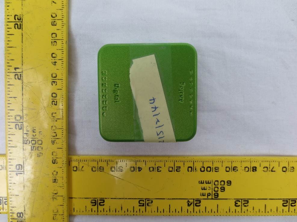
Click to zoom
Application Details
- Equipment Class
- DTS - Digital Transmission System
- Date of Grant
- Jan 27, 2016
- Application Purpose
- Original Equipment
- Date of Application
- Jan 27, 2016
- Equipment Note
- IoT Development Kit
- Frequency Range
- 2412.00000000 - 2462.00000000
- Company
- Marvell Semiconductor, Inc.
- Country
- United States
Documents & Files
Document Text
Text extracted from the exhibit documents filed with the FCC. Open a document above to read the original.
Users Manual
Kinoma Element User Guide About Kinoma Element The most important thing to know about Kinoma Element (shown in Figure 1) is that it is primarily a 3.3-volt system. If you are new to 3.3V systems or to hardware in general, this means that (unlike with an Arduino or some other boards), you can only send up to 3.3 volts into input pins on the device without doing damage to the pin. Figure 1. Kinoma Element Kinoma Element First Run Take these steps to get going on your Kinoma Element for the first time. Plug in Element with a moblie phone charger and micro USB cable. Use a high quality charger like the Apple iPhone charger. Element will boot automatically when powered. Element status light blinks red when booting. Element status light steady red when successfully booted and connected to a Wi-Fi network. Configuring the Kinoma Element xsEdit Download xsEdit. xsEdit has a GUI interface for adding the Kinoma Element network, setting the device name and pin configurations. xsEdit also is a Javascript editor and can push scripts wirelessly to your Kinoma Element. Command line You can configure your Kinoma Element via command line also. To do so connect the Kinoma Element to a PC/Laptop with a Micro-USB cable. In a Terminal application use the following commands. Get modem number ls /dev/tty.* The result will show the usbmodem number, add that to the following command sudo cu -l /dev/tty.usbmodem1421 After successfully connecting to the Kinoma Element use the following command to join a local Wi-Fi network. Kinoma Element will save the network configuration if a successful connection is made. Kinoma Element saves up to 10 Wi-Fi network profiles. connect YOUR-NETWORK-NAME wpa2 YOUR-NETWORK-PASSWORD 0 true Use the command: ip to view the Kinoma Elements current IP address ip Use the command: hostname to view the Kinoma Elements current device name. You can set the device name also with the hostname=YOUR-HOSTNAME command hostname hostname=YOUR-HOSTNAME Use the command: mac to view the Kinoma Element MAC address mac Te l e n t You can Telnet into a Kinoma Element by using the host name and .local 2323 telnet YOUR-HOSTNAME.local 2323 Powering Up/Down You can power down the Element by removing the micro-USB cable. Specifications Marvell MW302 200 MHz ARM Cortex M4 512 KB RAM 2.4 GHz Wi-Fi b/g /n 4 MB Flash 8 programmable Digital pins, supporting: Digital I²C PWM Serial SPI 8 programmable Analog pins, supporting: Analog All pins programmable to power or ground XS6 JavaScript engine with ES6 support Recommended operating temperature: -5°C to +50°C (23°F to 122°F) Compliance Statements FCC Statement This equipment has been tested and found to comply with the limits for a Class B digital device, pursuant to part 15 of the FCC Rules. These limits are designed to provide reasonable protection against harmful interference in a residential installation. This equipment generates, uses and can radiate radio frequency energy and, if not installed and used in accordance with the instructions, may cause harmful interference to radio communications. However, there is no guarantee that interference will not occur in a particular installation. If this equipment does cause harmful interference to radio or television reception, which can be determined by turning the equipment off and on, the user is encouraged to try to correct the interference by one or more of the following measures: Reorient or relocate the receiving antenna. Increase the separation between the equipment and receiver. Connect the equipment into an outlet on a circuit different from that to which the receiver is connected. Consult the dealer or an experienced radio/TV technician for help. FCC Radiation Exposure Statement This equipment complies with FCC RF radiation exposure limits set forth for an uncontrolled environment. This transmitter must not be co-located or operating in conjunction with any other antenna or transmitter. This equipment should be installed and operated with a minimum distance of 20 centimeters between the radiator and your body. This device complies with Part 15 of the FCC Rules. Operation is subject to the following two conditions: (1) this device may not cause harmful interference, and (2) this device must accept any interference received, including interference that may cause undesired operation. Caution! Any changes or modifications not expressly approved by the party responsible for compliance could void the user's authority to operate the equipment. Canada Statement This device complies with Industry Canada licence-exempt RSS standard(s). Operation is subject to the following two conditions: (1) this device may not cause interference, and (2) this device must accept any interference, including interference that may cause undesired operation of the device. Le présent appareil est conforme aux CNR d'Industrie Canada applicables aux appareils radio exempts de licence. L'exploitation est autorisée aux deux conditions suivantes : (1) l'appareil ne doit pas produire de brouillage, et (2) l'utilisateur de l'appareil doit accepter tout brouillage radioélectrique subi, même si le brouillage est susceptible d'en compromettre le fonctionnement. The device meets the exemption from the routine evaluation limits in section 2.5 of RSS 102 and compliance with RSS-102 RF exposure, users can obtain Canadian information on RF exposure and compliance. Le dispositif rencontre l'exemption des limites courantes d'évaluation dans la section 2.5 de RSS 102 et la conformité à l'exposition de RSS- 102 rf, utilisateurs peut obtenir l'information canadienne sur l'exposition et la conformité de rf. This transmitter must not be co-located or operating in conjunction with any other antenna or transmitter. This equipment should be installed and operated with a minimum distance of 20 centimeters between the radiator and your body. Cet émetteur ne doit pas être Co-placé ou ne fonctionnant en même temps qu'aucune autre antenne ou émetteur. Cet équipement dev…
Text truncated - open the document above for the full version.
External Photos
Marvell Semiconductor, Inc. FCC ID: UAYK501, IC: 6549A-K501 Report Number: R1512144-247 Page 72 of 76 FCC Part 15C/IC RSS-247 Test Report 14 Exhibit C - EUT Photographs 14.1 EUT Top View 14.2 EUT Bottom View Marvell Semiconductor, Inc. FCC ID: UAYK501, IC: 6549A-K501 Report Number: R1512144-247 Page 73 of 76 FCC Part 15C/IC RSS-247 Test Report 14.3 EUT Front View 14.4 EUT Rear View Marvell Semiconductor, Inc. FCC ID: UAYK501, IC: 6549A-K501 Report Number: R1512144-247 Page 74 of 76 FCC Part 15C/IC RSS-247 Test Report 14.5 EUT Right View 14.6 EUT Left View
Internal Photos
Marvell Semiconductor, Inc. FCC ID: UAYK501, IC: 6549A-K501 Report Number: R1512144-247 Page 75 of 76 FCC Part 15C/IC RSS-247 Test Report 14.7 EUT Open Case Top View 14.8 EUT Open Case Bottom View Antenna Marvell Semiconductor, Inc. FCC ID: UAYK501, IC: 6549A-K501 Report Number: R1512144-247 Page 76 of 76 FCC Part 15C/IC RSS-247 Test Report 14.9 Debugging Board Top View 14.10 Debugging Board Bottom View --- END OF REPORT ---
Operational Description
Kinoma Element Marvell Semiconductor Kinoma Element Hardware Technical Reference Manual Kinoma HW team 12/1/2015 Kinoma Element Hardware Revision K5R4 Page 1 Contents Kinoma Element Hardware Technical Reference Manual ............................................................................ 4 Photo of Kinoma Element PCB .................................................................................................................. 4 Block Diagram ........................................................................................................................................... 4 Power supply architecture ........................................................................................................................ 5 On chip power regulators ......................................................................................................................... 5 IO power ................................................................................................................................................... 5 Reference clocks ....................................................................................................................................... 6 Reset ......................................................................................................................................................... 6 User Button ............................................................................................................................................... 6 Micro USB OTG port .................................................................................................................................. 6 User connectors ........................................................................................................................................ 6 Power/Ground circuitry for User IO pins .................................................................................................. 6 Boot process ............................................................................................................................................. 8 Appendix A user pin to mw302 GPIO map ............................................................................................... 9 Appendix C Extension power unit connections ...................................................................................... 10 Appendix D understanding user IO pins ................................................................................................. 11 IO pin current capacity ........................................................................................................................ 11 Total system power budget ................................................................................................................ 11 Inductance of the wires ...................................................................................................................... 11 Stray capacitance on solderless breadboards..................................................................................... 11 I2C bus ................................................................................................................................................. 12 Reference documents ................................................................................................................................. 13 Kinoma Element Hardware Revision K5R4 Page 1 Figure 1 Element PCB assembly .................................................................................................................... 4 Figure 2 Element Block Diagram ................................................................................................................... 4 Figure 3 on board 5 volt to 3.3 volt switching supply ................................................................................... 5 Figure 4 MW302 on chip power supplies ..................................................................................................... 5 Figure 5 P and N channel mosfets ................................................................................................................ 7 Figure 6 serial in-parallel out shift registers ................................................................................................. 7 Figure 7 extension power connections ....................................................................................................... 10 Figure 8 logic state change vs voltage current change ............................................................................... 11 Figure 9 I2C bus pull up resistors in parallel ............................................................................................... 12 Kinoma Element Hardware Revision K5R4 Page 1 Kinoma Element Hardware Technical Reference Manual This document describe Kinoma Element Board circuit functions. Photo of Kinoma Element PCB Figure 1 Element PCB assembly Block Diagram Figure 2 Element Block Diagram Kinoma Element Hardware Revision K5R4 Page 1 Power supply architecture Element power supply has two main sections, system wide input from either micro USB connector or from dedicated J2 pins. Both inputs are tied together and feed on board 3.3 volt supply. Figure 3 on board 5 volt to 3.3 volt switching supply On chip power regulators MW302 contains on-chip power supplies for 1.8 volt and 1.1 volt. There are two sets of on chip power supplies, one for microcontroller part and another for wifi part. The 1.8 volt supply for wifi part is a switching supply controller utilizes L3. All other supplies are low drop out regulators that require output capacitor only. Figure 4 MW302 on chip power supplies IO power Element use 3.3 volt IO power for all signals including QSPI flash and sleep clock. Kinoma Element Hardware Revision K5R4 Page 1 Reference clocks System wide clock is derived from Y1 38.4 megahertz crystal. For the mw302 power management, a sleep clock os…
Text truncated - open the document above for the full version.
Schematics
55 44 33 22 11 D D C C B B A A Table of Contents P1 - Block DiagramP2 - MW300 SOC, antenna, Flash, sleep clockP3 - system power, USB OTG, buttons, LED, connector to dongle P5 - Flex connector #1 analog capable portP6 - Flex connector #2 digital only Optional Features JTAG access is provided for Development usehookup points for battery power and USB power switc h P99 - Change History MIcro USB OTG connector 5V to 3.3V switching supply 38.4MHzCrystal 32.768KHzOscillator 3.3 Volt 2.4GHz Wifi Antenna User ButtonRGB LED System Reset Button GPIO PWM UART/SPI/I2C GPIO/ANALOG PWM UART/SPI/I2C User IO PINS 1 to 8 User IO PINS 9 to 16 MW302 88 pin QFNMarvellWifi Microcontroller Wifi section Power1.8V switching1.1 V LDO MCU section Power1.8 V LDO1.1 V LDO IO Pin Power/Ground circuitry IO Pin Power/Ground circuitry 5.0 Volt 3.3 Volt Element DVT Schematics TitleSize Document Number Rev Date: Sheet of Marvell Technology Ltd Kinoma Element DVT 0 Kinoma ElementC 1 6 Monday, November 23, 2015 TitleSize Document Number Rev Date: Sheet of Marvell Technology Ltd Kinoma Element DVT 0 Kinoma ElementC 1 6 Monday, November 23, 2015 TitleSize Document Number Rev Date: Sheet of Marvell Technology Ltd Kinoma Element DVT 0 Kinoma ElementC 1 6 Monday, November 23, 2015 55 44 33 22 11 D D C C B B A A QSPI FLASH Johanson 2450AT18A100 88MW302 QFN-88 SoC Circuit analog capable IO <---PIN 1-8---> ----PIN 9-12--------PIN 13-16alternate---- P 13-16 ----Flex1pwr/gnd ctrl---- <-- Flex2 +/- ctrl power / ground controls Buttons and LEDs ----LEDsbuttons---- USB OTG and controls 32Megabits/4Megabytes STRAP1 not useddefault pull high STRAP0 SLEEP CLK UART0 - GPIO 3 & 2 K5R1 ECO#4 Clear ground impedance 50 ohmground reference on bottom layer ECO K5R3.1: VBUS fix V1P1 V1P8 V3P3 V1P8 V1P1 V3P3 V3P3 V3P3 V3P3 GND V3P3 V3P3 V3P3 V1P8 V1P8O V1P8O VBUS_OTG PIN1 4 PIN2 4 PIN3 4 PIN4 4 PIN5 4 PIN6 4 PIN7 4 PIN8 4 OE1 4 STR1 4 D_1_4 4 CP1 4 D_5_8 4 STR2 5 D_9_12 5 CP2 5 D_13_16 5 OE2 5 WAKEUP0 3 LED2 3 LED1 3 USB_DRVBUS 3 USB_OTG_POWER_FAULT 3 PIN9 5 PIN10 5 PIN11 5 PIN12 5 PIN13 5 PIN14 5 PIN15 5 PIN16 5 USB_DP 3 USB_DM 3 USB_ID 3 LED3 3 MCI_TRST 3 MCI_TMS 3 MCI_TDI 3 MCI_TDO 3 MCI_TCK 3 RESETn 3 TitleSize Document Number Rev Date: Sheet of Marvell Technology Ltd Kinoma Element DVT 0 SOCC 2 6 Monday, November 23, 2015 TitleSize Document Number Rev Date: Sheet of Marvell Technology Ltd Kinoma Element DVT 0 SOCC 2 6 Monday, November 23, 2015 TitleSize Document Number Rev Date: Sheet of Marvell Technology Ltd Kinoma Element DVT 0 SOCC 2 6 Monday, November 23, 2015 R25 1k C140.1uF C0201 R36.04k 1% R0201 C240.1uF C0201 C17 10uF 6.3V X5R C0402 C220.01uF C0201C90.1uF C0201 TP4 C510uF 6.3V X5RC0402 L3 2.2uH TP7 C40.01uF C0201 FB9 FB/3A C162.2uFC0402 C201.0uFC0201 C1510uF 6.3V X5RC0402 C230.01uF C0201 FB10 FB/3A L2*2.2nHL0402 C70.1uF C0201 R121 10K U2W25Q32FVZPIG CS 1 DO 2 WP 3 GND 4 DI 5 CLK 6 HOLD 7 VCC 8 EPAD 9 TP6 C190.01uF C0201 R451KR0201 C1210pF RFC0201 R651KR0201 C920.1uF C0201 C30.1uF C0201C270.1uF C0201 C2 2.2uF C0402 C290.1uF C930.1uF C0201 C250.01uF C0201 C181.0uFC0201 C100.1uF C0201 C95*0.1uF C0201 R751KR0201 MOV1CDS305GTA 12 C80.1uF C0201C130.1uF C0201 R128 22R R0201 C210.01uF C0201 FL1 LFB182G45CL3D178 IN 1 OUT 3 GND 2 C98 0.01uF C0201 Y2 32.768KHz_3.3V_+/-25ppm EC 1 GND 2 OUT 3 VDD 4 C60.1uF C0201C280.1uF C0201 TP5 R551KR0201 C1 2.2uF C0402 88MW302QFN88 U1 GPIO_0 1 GPIO_1 2 GPIO_2 3 GPIO_3 4 VDDIO_0 5 GPIO_4 6 GPIO_5 7 GPIO_6 8 GPIO_7 9 GPIO_8 10 GPIO_9 11 GPIO_10 12 GPIO_11 13 GPIO_12 14 GPIO_13 15 GPIO_14 16 GPIO_15 17 AVDD18 18 AVDD18 19 AVDD33 20 RF_TR 21 NC 22 USB_DM 65 USB_DP 64 USB_AVDD33 63 USB_ID 62 USB_VBUS 61 VTR_VDD33 60 VDD11 59 VDDIO_2 58 GPIO_33 57 GPIO_32 56 GPIO_31 55 GPIO_30 54 GPIO_29 53 GPIO_28 52 VDDIO_AON 51 GPIO_26 50 GPIO_25 49 GPIO_24 48 GPIO_23 47 GPIO_22 46 RESETn 45 FLY11 88 VBAT_IN 87 FLY18 86 GPIO_49 85 GPIO_48 84 GPIO_47 83 GPIO_46 82 GPIO_45 81 GPIO_44 80 GPIO_43 79 GPIO_42 78 VDDIO_3 77 GPIO_41 76 GPIO_40 75 ISENSE 74 VDDIO_3 73 GPIO_39 72 GPIO_38 71 GPIO_37 70 GPIO_36 69 GPIO_35 68 GPIO_34 67 GPIO_27 66 AVDD18 23 AVDD18 24 AVDD18 25 XTAL_IN 26 XTAL_OUT 27 AVDD18 28 DNC29 29 DNC30 30 DNC31 31 DNC32 32 VDD11 33 VDDIO_1 34 GPIO_16 35 GPIO_17 36 GPIO_18 37 GPIO_19 38 GPIO_20 39 GPIO_21 40 LDO11_VOUT 41 LDO11_V18 42 BUCK18_VX 43 VBAT_IN 44 EPAD 89 ANT12450AT18A100 L52.2nHL0402 Y1 38.4MHz +/-10ppm IN 1 GND 2 OUT 3 GND 4 C260.01uF C0201 L12.2nHL0402 VDD33_20 VIO1_34VIO-AON_51VIO2_58VDD33_60VDD33_63VIO3N_73VDD33_87 VDD11_F_88 VDD18_F_86 VDD18_24 VDD18_28 VDD18_19VDD18_18VDD11_33VDD18_23VDD11_59VIO3_77VIO0_5VDD18_25 VDD33_44 VIO0_5VDD33_20 VIO1_34 VIO-AON_51VIO2_58 VIO3N_73 VIO3_77 VDD33_87 VDD18_F_86 VDD11_F_88 VDD18_18VDD18_19 VDD18_23 VDD18_24 VDD18_25 VDD18_28 VDD11_33 VDD11_59RESETNUSB_DMUSB_DPVDD33_63VDD33_60USB_IDUSB_VBUS GPIO_44 GPIO_45 ISENSE ISENSE QSPI_SSnQSPI_D3QSPI_D2QSPI_D1QSPI_D0QSPI_CLK XTAL_IN XTAL_OUT GPIO_0GPIO_1GPIO_2GPIO_3 GPIO_4 GPIO_7 GPIO_6GPIO_5 GPIO_8GPIO_11GPIO_10GPIO_9GPIO_12GPIO_15GPIO_14GPIO_13 GPIO_16 GPIO_17 GPIO_18 GPIO_19 GPIO_20 GPIO_21 GPIO_22GPIO_23GPIO_24GPIO_27 GPIO_34 GPIO_35 GPIO_36 GPIO_37 GPIO_38 GPIO_39 GPIO_40 GPIO_41 GPIO_42 GPIO_43 GPIO_46 GPIO_47 GPIO_48 GPIO_49 QSPI_SSnQSPI_D1QSPI_D2 QSPI_D3QSPI_CLKQSPI_D0 GPIO_26GPIO_25 QSPI_SSnQSPI_D2QSPI_D3 GPIO_42 PIN1 GPIO_43 PIN2 GPIO_45 PIN4 GPIO_44 PIN3 GPIO_48 PIN7 GPIO_47 PIN6 GPIO_46 PIN5 GPIO_49 PIN8 GPIO_11GPIO_12GPIO_14GPIO_15GPIO_13 GPIO_22 GPIO_23GPIO_34GPIO_4GPIO_16GPIO_17 GPIO_41 GPIO_26GPIO_39 CLK32K GPIO_40 PIN9 GPIO_0 PIN10 GPIO_1 PIN12 GPIO_3 PIN11 GPIO_2 PIN15 GPIO_20 PIN13 GPIO_18 PIN16 GPIO_21 PIN14 GPIO_19 GPIO_27 EN_32K USB_DPUSB_DMUSB_ID GPIO_38 GPIO_8GPIO_7GPIO_6GPIO_9GPIO_10 RF_TX-RX GPIO_25 55 44 33 22 11 D D C C B B A A APPLICATION RGB LED PUSH BUTTONS RESETn WAKE0 FTDI, USB OTG JTAG on dongle for development Battery Hookup USB power switch moved to battery board ECO K5R3.4: depopulate two pin connector MOD: need for reset fix GND_OTG_CONN GND_OTG_CONN VBUS_OTG VBUS_OTG VBUS_OTG_CONN GND_OTG_CO…
Text truncated - open the document above for the full version.
Test Report
Note: This test report is prepared for the customer shown above and for the device described herein. It may not be duplicated or used in part without prior written consent from Bay Area Compliance Laboratories Corp. This report must not be used by the customer to claim product certification, approval, or endorsement by A2LA*, NIST, or any agency of the Federal Government. * This report may contain data that are not covered by the A2LA accreditation and are marked with an asterisk “*” (Rev.2) FCC PART 15, SUBPART C IC RSS-247, ISSUE 1, MAY 2015 TEST AND MEASUREMENT REPORT For Marvell Semiconductor, Inc. 5488 Marvell Lane, Santa Clara, CA 95054, USA FCC ID: UAYK501 IC: 6549A-K501 Report Type: Original Report Product Type: Software Development Kit with Wi-Fi Connectivity Prepared By: Leonard Gray Associate En gineer Report Number: R1512144-247 Report Date: 2016-01-27 Reviewed By: Bo Li RF Su pervisor Bay Area Compliance Laboratories Corp. 1274 Anvilwood Avenue, Sunnyvale, CA 94089, USA Tel: (408) 732-9162 Fax: (408) 732-9164 Marvell Semiconductor, Inc. FCC ID: UAYK501, IC: 6549A-K501 Report Number: R1512144-247 Page 2 of 76 FCC Part 15C/IC RSS-247 Test Report TABLE OF CONTENTS 1 General Description ..................................................................................................................................................... 5 1.1 Product Description for Equipment Under Test (EUT) ...................................................................................... 5 1.2 Mechanical Description of EUT ......................................................................................................................... 5 1.3 Objective ............................................................................................................................................................. 5 1.4 Related Submittal(s)/Grant(s) ............................................................................................................................. 5 1.5 Test Methodology ............................................................................................................................................... 5 1.6 Measurement Uncertainty ................................................................................................................................... 5 1.7 Test Facility ........................................................................................................................................................ 6 2 System Test Configuration.......................................................................................................................................... 7 2.1 Justification ......................................................................................................................................................... 7 2.2 EUT Exercise Software....................................................................................................................................... 7 2.3 Equipment Modifications.................................................................................................................................... 9 2.4 Local Support Equipment ................................................................................................................................... 9 2.5 EUT Internal Configuration Details .................................................................................................................... 9 2.6 Power Supply and Line Filter ............................................................................................................................. 9 2.7 Interface Ports and Cabling ................................................................................................................................. 9 3 Summary of Test Results ............................................................................................................................................ 10 4 FCC §15.247(i) & IC RSS §102 – RF Exposure ........................................................................................................ 11 4.1 Applicable Standards ........................................................................................................................................ 11 4.2 MPE Prediction ................................................................................................................................................. 12 4.3 MPE Results for FCC ....................................................................................................................................... 12 4.4 RF exposure evaluation exemption for IC ........................................................................................................ 12 5 FCC §15.203 & IC RSS-Gen §8.3 - Antenna Requirements .................................................................................... 13 5.1 Applicable Standards ........................................................................................................................................ 13 5.2 Antenna List and Details ................................................................................................................................... 13 6 FCC §15.207 & IC RSS-Gen §8.8 – AC Line Conducted Emissions ....................................................................... 14 6.1 Applicable Standards ........................................................................................................................................ 14 6.2 Test Setup ......................................................................................................................................................... 14 6.3 Test Procedure .................................................................................................................................................. 14 6.4 Test Setup Block Diagram ..................................................................…
Text truncated - open the document above for the full version.
Test Setup Photos
Marvell Semiconductor, Inc. FCC ID: UAYK501, IC: 6549A-K501 Report Number: R1512144-247 Page 69 of 76 FCC Part 15C/IC RSS-247 Test Report 13 Exhibit B - Test Setup Photographs 13.1 Radiated Emission below 1 GHz Front View 13.2 Radiated Emission below 1 GHz Rear View Marvell Semiconductor, Inc. FCC ID: UAYK501, IC: 6549A-K501 Report Number: R1512144-247 Page 70 of 76 FCC Part 15C/IC RSS-247 Test Report 13.3 Radiated Emission above 1 GHz Front View 13.4 Radiated Emission above 1 GHz Rear View Marvell Semiconductor, Inc. FCC ID: UAYK501, IC: 6549A-K501 Report Number: R1512144-247 Page 71 of 76 FCC Part 15C/IC RSS-247 Test Report 13.5 AC Line Conducted Emission Front View 13.6 AC Line Conducted Emission Side View
Contact Information
Applicant
Ken Wu
Test Firm
Bay Area Compliance Laboratories Corp.Lisa Tang
Technical Specifications
| # | Rule Parts | Frequency Range | Power Output |
|---|---|---|---|
| 1 | 15C | 2.41 GHz - 2.46 GHz | 5.00 mW |
Other Applications from Marvell Semiconductor, Inc.
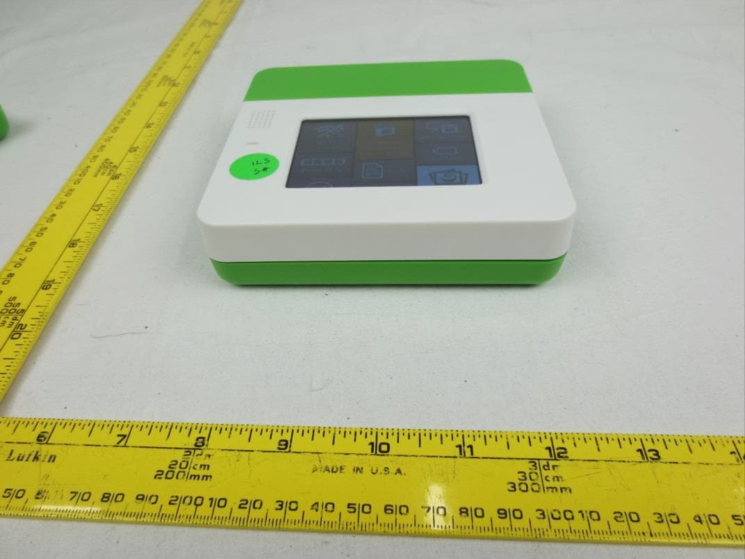
UAYK402
Dec 02, 2015IoT Development Kit
Equipment Class
NII - Unlicensed National Information Infrastructure TX
UAY-MC8687P
Jan 16, 2008MC8687P Mini Card 802.11 b/g Radio Card
Equipment Class
DTS - Digital Transmission System
UAY-MMC85M
Jul 17, 2006MC85 Mini Card 11b/g/a/n Radio Card
Equipment Class
DTS - Digital Transmission System