XDY-ESEALV2Bolt for Wireless Container Security
System Planning Corporation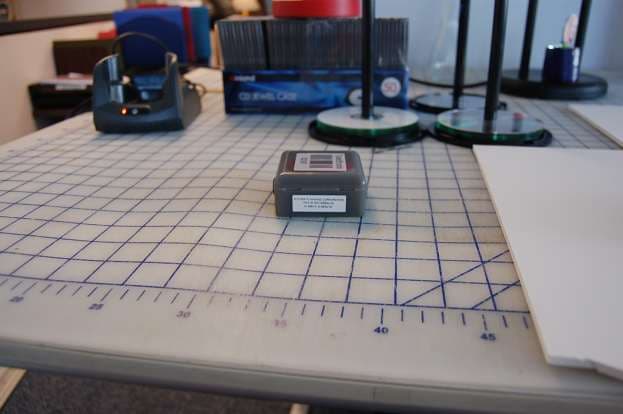
Click to zoom
Application Details
- Equipment Class
- DTS - Digital Transmission System
- Date of Grant
- Jun 07, 2012
- Application Purpose
- Original Equipment
- Date of Application
- Jun 07, 2012
- Equipment Note
- Bolt for Wireless Container Security
- Frequency Range
- 2405.00000000 - 2475.00000000
- Company
- System Planning Corporation
- Country
- United States
Documents & Files
Document Text
Text extracted from the exhibit documents filed with the FCC. Open a document above to read the original.
Users Manual
GlobalTrak™ Assembly 203026, E‐Seal with ZigBee Interface V2 Operation Manual Prepared: J. Carn Date: May 24, 2012 Page 1 of 11 GlobalTrak™ Assembly 203026, E‐Seal with ZigBee Interface V2 Operation Manual System Planning Corporation 3601 Wilson Boulevard Arlington, VA 22201 (703) 351‐8700 www.globaltrak.com www.sysplan.com [email protected] GlobalTrak™ Assembly 203026, E‐Seal with ZigBee Interface V2 Operation Manual Prepared: J. Carn Date: May 24, 2012 Page 2 of 11 GlobalTrak™ Assembly, E‐Seal with ZigBee Interface V2 Operation Manual The purpose of the GlobalTrak™ Assembly, E‐Seal with ZigBee Interface V2 Operation Manual is to: • Familiarize the user with the functions and capabilities of the GlobalTrak E‐Seal with ZigBee Interface V2 • Provide a guide for operation procedures for the GlobalTrak E‐Seal with ZigBee Interface V2 GlobalTrak™ Assembly 203026, E‐Seal with ZigBee Interface V2 Operation Manual Prepared: J. Carn Date: May 24, 2012 Page 3 of 11 Table of Contents 1.0 GlobalTrak E‐Seal with ZigBee Interface V2 Overview ............................................................................ 4 1.1: GlobalTrak E‐Seal with ZigBee Interface V2 Overview ................................................................................ 4 1.2: Feature List .................................................................................................................................................. 6 2.0: Using the GlobalTrak E‐Seal with ZigBee Interface V2 ............................................................................... 7 2.1: Device Power Instructions .......................................................................................................................... 7 2.1.1: Power On ................................................................................................................................................ 7 2.1.2: Power Off ................................................................................................................................................ 8 2.2: Installation .................................................................................................................................................. 9 2.3: Removal & Deactivation ........................................................................................................................... 10 GlobalTrak™ Assembly 203026, E‐Seal with ZigBee Interface V2 Operation Manual Prepared: J. Carn Date: May 24, 2012 Page 4 of 11 1.0 GlobalTrak E‐Seal with ZigBee Interface V2 Overview 1.1: GlobalTrak E‐Seal with ZigBee Interface V2 Overview The GlobalTrak E‐Seal with ZigBee Interface V2 provides enhanced security capability to the GlobalTrak Asset Monitoring Units using a CT‐PAT electronic barrier seal. Users have the ability to monitor real‐time location and seal status on a variety of assets, including intermodal containers, trailers, semi‐trailers, and rail cars. When the bolt is cut, a notification is generated. The GlobalTrak E‐Seal with ZigBee Interface V2 is used in conjunction with any of the GlobalTrak Asset Monitoring Units. The assembly consists of three components: • Body of the GlobalTrak E‐Seal with ZigBee Interface V2 • Bolt • Locking Cap Figure 1. Body of the GlobalTrak E‐Seal with ZigBee Interface V2 GlobalTrak™ Assembly 203026, E‐Seal with ZigBee Interface V2 Operation Manual Prepared: J. Carn Date: May 24, 2012 Page 5 of 11 Figure 2. Bolt Figure 3. Locking Cap GlobalTrak™ Assembly 203026, E‐Seal with ZigBee Interface V2 Operation Manual Prepared: J. Carn Date: May 24, 2012 Page 6 of 11 1.2: Feature List The product is designed to provide additional security information for assets monitored by Asset Monitoring Units. This is accomplished by equipping the GlobalTrak E‐Seal with ZigBee Interface with the following features: a) ZigBee Wireless: The wireless standard for low‐power short‐range bi‐directional communications, suitable for mesh networks and sensor reads. Line‐of‐sight of up to 250 meters. b) Long Battery Life: Non‐rechargeable lithium thionyl chloride battery can remain active for a minimum of 180 days. Shelf life up to 3 years. c) Physical Security: Barrier‐type bolt seal requires more than 2,000 lbs (907 kgs; kN) of pull‐out strength. d) Location Reporting: The on‐board high sensitivity of Assisted GPS receiver calculates its position within a few meters of accuracy even from within containers or trailers. e) Environmental robustness: Can operate across a spectrum of temperatures (‐20°C to +70°C) and up to 95% humidity (non‐condensing at +70°C) GlobalTrak™ Assembly 203026, E‐Seal with ZigBee Interface V2 Operation Manual Prepared: J. Carn Date: May 24, 2012 Page 7 of 11 2.0: Using the GlobalTrak E‐Seal with ZigBee Interface V2 2.1: Device Power Instructions 2.1.1: Power On 1. Insert the bolt into the hole on the side that says “enter”. Figure 4. Insert Bolt 2. Red and yellow LEDs will flash until the GlobalTrak E‐Seal with ZigBee Interface V2 begins communicating with a GlobalTrak Asset Monitoring Unit. The GlobalTrak E‐Seal with ZigBee Interface V2 will search for up to four minutes. Note : If the GlobalTrak E‐Seal with ZigBee Interface V2 is not within the vicinity of an Asset Monitoring Unit, and if the LEDs stop flashing prematurely, the battery may be low. GlobalTrak™ Assembly 203026, E‐Seal with ZigBee Interface V2 Operation Manual Prepared: J. Carn Date: May 24, 2012 Page 8 of 11 Figure 5a & 5b. Searching for Asset Monitoring Unit. LEDs flashing. 2.1.2: Power Off 1. Remove the bolt and wait for the red LED to flash twice. Figure 6. Remove bolt, red LED flashes twice. 2. Insert the bolt again, and remove it after 1‐3 seconds. Note : A solid red light will show for 3 seconds, indicating that the device will shut down after sending a shutdown message. GlobalTrak™ Assembly 203026, E‐Seal with ZigBee Interface V2 Operation Manual Prepared: J. Carn Date: May 24, 2012 Page 9 of 11 2.2: Installation 1. Close container door. 2…
Text truncated - open the document above for the full version.
Block Diagram
24 MHz Crystal Oscillator EM250 Radio Transceiver Integrated On- Board F Antenna 24 MHz 2.4 GHz Block Diagram taken from EM250 Datasheet (www.ember.com) The only RF design done by SPC is the addition of the oscillator to the circuit. All other RF is done in the chip, designed by Ember.
Internal Photos
Photograph 1. E-Seal PCB Top Photograph 2. E-Seal PCB Bottom Photograph 3. E-Seal PCB Box Open Photograph 4. E-Seal PCB Box Closed
Operational Description
GlobalTrak Assembly 203026, E‐Seal with ZigBee Interface V2 Operational Description The GlobalTrak Assembly 203026, E‐Seal with ZigBee Interface V2 provides enhanced security for GlobalTrak Asset Monitoring Units. It is a CT‐PAT electronic barrier seal that is used in conjunction with an Asset Monitoring Unit, and not as a standalone device. It communicates position and seal status via ZigBee, and will generate a notification when the bolt seal is cut.
Parts List/Tune Up Info
PARTS LIST SYSTEM PLANNING CORPORATION PL - 203025-01 REVISION: B ---------- 1000 WILSON BLVD --------------------- REV DATE: 03/2 5/11 ARLINGTON, VA 22209 CAGE NO.: 9G490 LIST DATE: 03/2 5/11 LIST TITLE: PCB ASSEMBLY,E-SEAL WITH ZIGBEE INTERFACE, GLOBAL TRAK PAGE: 1 O F 4 ------------------------------------------------------------------------------------------------------------------------------- ----- ITEM CAGE COMPONENT COMPONENT MFG ID MANUFACTURER NAME SUB NO REQ QTY U/M REFERENCE DESIGNATORS NO. /SUBSTITUTE DESCRIPTION MANUFACTURER PART NO ASY --- -------- --- -------------------------- ----- ---------------- ------------------------- ------ ----------------------- - --- 3 0.00 EA 302033 SCHEMATIC, E-SEAL WITH 190033 SYSTEM PLANNING CORP. N ZIGBEE INTERFACE, GLOBAL 302033 TRAK 5 1.00 EA 406309-01 PCB, E-SEAL WITH 190033 SYSTEM PLANNING CORP. N ZIGBEE INTERFACE, GLOBAL 406309-01 TRAK 8 1.00 EA U1 EM250-RTR(+BTLD* IC,EM250,WITH BOOTLOADER EMBER EMBER N SOL, QFN-48, ZIGBEE/ EM250-RTR(+BTLDR) 802.15.4 spcdoc SPC DOCUMENT 854673 9 1.00 EA BT1 15-4903-53000 BATTERY, AA, 3.6V, 2.4AH TADIRA TADIRAN N MODEL TL-4903, LITHIUM,W/ 15-4903-53000 POL-TABS spcdoc SPC DOCUMENT 853357 10 1.00 EA Y1 ABM3B-24.000MHZ* IC, CRYSTAL, 24.000MHz, ABRACO ABRACON CORPROATION N SMD ABM3B-24.000MHZ-D-R60-1 WT spcdoc SPC DOCUMENT 854027 11 0.00 EA (DNI: J2) FTSH-105-01-F-DV CONNECTOR, MICRO-HEADER, SAMTEC SAMTEC ELECTRONICS N 10 PIN, FTSH SERIES, .05 FTSH-105-01-F-DV PITCH spcdoc SPC DOCUMENT 853912 12 1.00 EA J3 PPPC041LGBN-RC CONNECTOR, FEMALE SOCKET SULLIN SULLINS CONNECTORS N 4 POSITION, R/A, 0.100" PPPC041LGBN-RC PITCH,GOLD spcdoc SPC DOCUMENT 854594 13 0.00 EA (DNI: J1) 102972-2 CONNECTOR-BREAKAWAY, AMP AMP INCORPORATED N SINGLEN ROW, VERTICLE, 2 102972-2 POSITION spcdoc SPC DOCUMENT 850267 14 1.00 EA DS1 LS L29K-H1J2-1 LED, SURFACE MOUNT CHIP, OSRAM OSRAM N RED, 630NM, 0603 LS L29K-H1J2-1 spcdoc SPC DOCUMENT 854644 16 1.00 EA DS2 LO L29K-J2L1-24 LED, SURFACE MOUNT CHIP, OSRAM OSRAM N ORANGE, 630NM, 0603 LO L29K-J2L1-24 PARTS LIST SYSTEM PLANNING CORPORATION PL - 203025-01 REVISION: B ---------- 1000 WILSON BLVD --------------------- REV DATE: 03/2 5/11 ARLINGTON, VA 22209 CAGE NO.: 9G490 LIST DATE: 03/2 5/11 LIST TITLE: PCB ASSEMBLY,E-SEAL WITH ZIGBEE INTERFACE, GLOBAL TRAK PAGE: 2 O F 4 ------------------------------------------------------------------------------------------------------------------------------- ----- ITEM CAGE COMPONENT COMPONENT MFG ID MANUFACTURER NAME SUB NO REQ QTY U/M REFERENCE DESIGNATORS NO. /SUBSTITUTE DESCRIPTION MANUFACTURER PART NO ASY --- -------- --- -------------------------- ----- ---------------- ------------------------- ------ ----------------------- - --- spcdoc SPC DOCUMENT 854645 19 1.00 EA L3 LQG18HN2N7S00D INDUCTOR, 2.7NH, +/-0.3 MURATA MURATA ERIE N NH, 300mA, 0603 MULTI- LQG18HN2N7S00D LAYER FILM spcdoc SPC DOCUMENT 853851 20 1.00 EA L2 LQG18HN3N3S00D INDUCTOR, 3.3nH, +/- 0.3 MURATA MURATA ERIE N nH, MULTILAYER FILM, LQG18HN3N3S00D 0603 spcdoc SPC DOCUMENT 851670 21 1.00 EA L23 LQP15MN2N0B02 INDUCTOR, 2.0NH, +/-0.1 MURATA MURATA ERIE N NH, 220mA, CHIP FILM, LQP15MN2N0B02 0402 spcdoc SPC DOCUMENT 853852 24 2.00 EA L1,L4 LQP15MN5N1B02 INDUCTOR, 5.1NH, +/-0.1 MURATA MURATA ERIE N NH, 140mA, CHIP FILM, LQP15MN5N1B02 0402 spcdoc SPC DOCUMENT 853849 27 1.00 EA CR1 MMBZ5V6AL-7 DIODE, DUAL SURFACE MT, DIODES DIODES, INC. N TVS, 3VOLT, 24WATT, MMBZ5V6AL-7 SOT-23 spcdoc SPC DOCUMENT 853364 29 1.00 EA FB1 BLM15HG102SN1D BEAD, FERRITE, FILTER MURATA MURATA ERIE N CHIP, 1000 OHM, 250mA, BLM15HG102SN1D 0402 spcdoc SPC DOCUMENT 853860 30 1.00 EA CR2 FDLL4148 DIODE, SMALL SIGNA, HI FAIRCH FAIRCHILD SEMICONDUCTOR N CONDUCTANCE, 100 VOLT, FDLL4148 LL-34 spcdoc SPC DOCUMENT 853363 31 2.00 EA R1,R4 ERJ-2GEJ103X RESISTOR, CHIP, 10K OHM, PANAS PANASONIC ELECTRONICS N 5%, 1/16 WATT, 0402 PACK ERJ-2GEJ103X SMD spcdoc SPC DOCUMENT 853853 32 1.00 EA R9 ERJ-2GEJ2R7X RESISTOR, CHIP, 2.7 OHM, PANAS PANASONIC ELECTRONICS N 5%, 1/16 WATT, 0402 PACK ERJ-2GEJ2R7X SMD spcdoc SPC DOCUMENT PARTS LIST SYSTEM PLANNING CORPORATION PL - 203025-01 REVISION: B ---------- 1000 WILSON BLVD --------------------- REV DATE: 03/2 5/11 ARLINGTON, VA 22209 CAGE NO.: 9G490 LIST DATE: 03/2 5/11 LIST TITLE: PCB ASSEMBLY,E-SEAL WITH ZIGBEE INTERFACE, GLOBAL TRAK PAGE: 3 O F 4 ------------------------------------------------------------------------------------------------------------------------------- ----- ITEM CAGE COMPONENT COMPONENT MFG ID MANUFACTURER NAME SUB NO REQ QTY U/M REFERENCE DESIGNATORS NO. /SUBSTITUTE DESCRIPTION MANUFACTURER PART NO ASY --- -------- --- -------------------------- ----- ---------------- ------------------------- ------ ----------------------- - --- 853858 33 1.00 EA R3 ERJ-3EKF1001V RESISTOR, 1K OHM, 1/16 PANAS PANASONIC ELECTRONICS N WATT, 1%, SMD, 0603, ERJ-3EKF101V spcdoc SPC DOCUMENT 851466 34 2.00 EA R5,R7 ERJ-2GEJ1R0X RESISTOR, CHIP, 1 OHM, PANAS PANASONIC ELECTRONICS N 5%, 1/16 WATT, 0402 PACK ERJ-2GEJ1R0X SMD spcdoc SPC DOCUMENT 853855 35 1.00 EA R6 ERJ-2GEJ332X RESISTOR, CHIP, 3.3K OHM PANAS PANASONIC ELECTRONICS N 5%, 1/10 WATT, 0402 PACK ERJ-2GEJ332X SMD spcdoc SPC DOCUMENT 853856 36 1.00 EA R2 ERJ2GEJ561X RESISTOR, 560 OHM, PANAS PANASONIC ELECTRONICS N 1/16 WATT, 5%, SMD, 0402 ERJ2GEJ561X PACK spcdoc SPC DOCUMENT 854854 37 1.00 EA R8 ERJ-2RKF1693X RESISTOR, CHIP, 169K OHM PANAS PANASONIC ELECTRONICS N 1%, 1/16 WATT, 0402 PACK ERJ-2RKF1693X SMD spcdoc SPC DOCUMENT 853857 38 2.00 EA R10,R11 ERJ-2GEJ102X RESISTOR, 1.0K OHM, PANAS PANASONIC ELECTRONICS N 1/16 WATT, 5%, SMD, 0402 ERJ-2GEJ102X PACK spcdoc SPC DOCUMENT 854008 39 1.00 EA R12 ERJ-6GEYJ104V RESISTOR, CHIP, 100K OHM PANAS PANASONIC ELECTRONICS N 5%, 1/8 WATT, 0805 PACK, ERJ-6GEYJ104V SMD spcdoc SPC DOCUMENT 852916 40 3.00 EA C7,C8,C9 GRM155R71C104KA* CAPACITOR, 0.1UF, 16VOLT MURATA MURATA ERIE N +/- 10%, X7R, 0402 GRM1555R71C104KA88D spcdoc SPC DOCUMENT 853843 42 3.00 EA C24,C25,C58 ECJ-0EC1H010C CAPACITOR, CHIP,…
Text truncated - open the document above for the full version.
Parts List/Tune Up Info
PARTS LIST SYSTEM PLANNING CORPORATION PL - 203026-01 REVISION: - ---------- 1000 WILSON BLVD --------------------- REV DATE: 10/0 1/09 ARLINGTON, VA 22209 CAGE NO.: 9G490 LIST DATE: 11/1 6/10 LIST TITLE: ASSEMBLY, E-SEAL WITH ZIGBEE INTERFACE, V2, GLOBALTRAK PAGE: 1 O F 1 ------------------------------------------------------------------------------------------------------------------------------- ----- ITEM CAGE COMPONENT COMPONENT MFG ID MANUFACTURER NAME SUB NO REQ QTY U/M REFERENCE DESIGNATORS NO. /SUBSTITUTE DESCRIPTION MANUFACTURER PART NO ASY --- -------- --- -------------------------- ----- ---------------- ------------------------- ------ ----------------------- - --- 3 0.00 EA 302033 SCHEMATIC, E-SEAL WITH 190033 SYSTEM PLANNING CORP. N ZIGBEE INTERFACE, GLOBAL 302033 TRAK 4 1.00 EA 78489 LABEL, GTID, WITH CODE SETON SETON LABELS N 39 BARCODE, MONDO-BONDO, 78489 WHITE spcdoc SPC DOCUMENT 853581 5 1.00 EA A1 203025-01 PCB ASSEMBLY,E-SEAL WITH 190033 SYSTEM PLANNING CORP. Y ZIGBEE INTERFACE, GLOBAL 203025-01 TRAK 10 1.00 EA 1950330 E-SEAL BOX EJBROO EJ BROOKS N 1950330 spcdoc SPC DOCUMENT 853477 11 1.00 EA 1950210 LID, E-SEAL BOX EJBROO EJ BROOKS N 1950210 spcdoc SPC DOCUMENT 853478 25 1.00 EA EJ BROOKS LABEL LABEL, EJ BROOKS, FOR EJBROO EJ BROOKS N 202867-01, ZIGBEE,E-SEAL TBD spcdoc SPC DOCUMENT 853936 39 1.00 EA PTL-29-489 LABEL, BRADYBONDZ, WHITE BRADY BRADY N POLYESTER, 1.50"W, 0.50" PTL-29-489 HEIGHT spcdoc SPC DOCUMENT 853496 TOTAL NO PAGES: 1
RF Exposure Info
Page 1 Designing with an Inverted-F PCB Antenna For the EM250 and EM260 Platforms This document describes an Inverted-F PCB antenna designed by Ember for use with both the EM250 and EM260. The Inverted-F antenna is one of the more commonly used antennas at 2.4 GHz. Ember provides antenna dimensions in two different substrate thicknesses. PCB antennas are board specific, so you may need to modify the antenna dimensions for your board implementation. Contents Overview .............................................................................................. 2 Layout ................................................................................................. 2 Key features ....................................................................................... 2 Board stackup...................................................................................... 3 Tuning and Antenna Placement ................................................................... 4 Antenna placement ............................................................................... 4 Tuning............................................................................................... 5 Antenna pattern simulations .................................................................... 6 Antenna Performance ............................................................................... 6 Effects of manufacturing variations............................................................ 8 Measured antenna patterns ..................................................................... 9 Antenna patterns for EM250 62 mil boards .................................................. 10 Antenna patterns for EM260 62 mil boards .................................................. 11 Antenna patterns for EM250 0.8mm boards.................................................. 12 Antenna patterns for EM260 0.8mm boards.................................................. 13 Application Note 5052 14 February 2008 120-5052-000A Page 2 Designing with an Inverted-F PCB Antenna 120-5052-000A Overview One of the main reasons to use a PCB antenna is to reduce cost. Since the antennas are printed directly on the board, they are generally considered to be free. On boards with room to spare, this will be true. On boards that need to grow to account for the increased size of the printed antenna, you must include the added cost of the larger PCB when calculating cost savings. Well-implemented PCB antennas will have similar performance to that of a ceramic antenna. Ember has released the following Inverted-F based Reference Designs: • EM250 4-Layer Design, Inverted-F Antenna, 0.062′′ thick (EM250_REF_DES_LC_LAT_INV-F_62mil.zip) • EM250 4-Layer Design, Inverted-F Antenna, 0.8mm thick (EM250_REF_DES_LC_LAT_INV-F_0.8mm.zip) • EM260 4-Layer Design, Inverted-F Antenna, 0.062′′ thick (EM260_REF_DES_LC_LAT_INV-F_62mil.zip) • EM260 4-Layer Design, Inverted-F Antenna, 0.8mm thick (EM260_REF_DES_LC_LAT_INV-F_0.8mm.zip) Layout PCB antennas are very layout sensitive. For best performance, Ember recommends following the reference design layouts as closely as possible. Key features Some key features of the design include the following: • There are two versions of the layout: for the 62 mil and 0.8mm board thicknesses • Feed arm should be fed with a 50-Ohm microstrip transmission line (14 mils for an 0.008′′ top layer) • Shorting arm must be shorted to the ground plane, preferably with two ground vias • There should be no ground plane under the antenna • Ground plane on layers 2 and 4, with stitching vias along the ground edge • No ground pour on layer 1 • The antenna was designed to have a 40 mil clearance between the shorting arm and the board edge, and a 20 mil clearance between the board edge and the antenna trace • The antenna should be covered with soldermask • Simulations have shown no benefit to increasing the width of the shorting arm or mitering the bend in the shorting arm Figure 1 illustrates the dimensions of the antenna. Page 3 Designing with an Inverted-F PCB Antenna 120-5052-000A 0.782" 0.040" 0.040" 0.109" 0.039" 0.040" 0.020" 0.327" 0.020" Inverted-F Antenna Dimensions For 0.062" FR4 Substrate 0.050" (Antenna can be mirrored) Place vias along ground plane edge with approximately 50 mil spacing to stitch layers 2 and 4 together Board Edge Board Edge 50 ohm Antenna shorting arm should be grounded with 2 vias 0.860" 0.040" 0.040" 0.115" 0.039" 0.040" 0.020" 0.311" 0.020" Inverted-F Antenna Dimensions For 0.8mm FR4 Substrate 0.050" (Antenna can be mirrored) Place vias along ground plane edge with approximately 50 mil spacing to stitch layers 2 and 4 together Board Edge Board Edge 50 ohm Antenna shorting arm should be grounded with 2 vias Figure 1. Antenna dimensions Note: You may need to modify dimensions for your board’s implementation. Board stackup Figure 2 shows the board stackups used in the designs. Page 4 Designing with an Inverted-F PCB Antenna 120-5052-000A (a) Total Thickness 0.062" (b) Total Thickness 0.8mm Layer Stackup Total Thickness = 0.034" +/- 10% 0.008" FR4 0.008" FR4 0.016" FR4 *** *** Material thickness between Layer 2 and Layer 3 may be adjusted to meet Total Thickness requirement. Layer 1 (1/2 oz) Layer 2 (1 oz) Layer 3 (1 oz) Layer 4 (1/2 oz) 0.008" FR4 0.008" FR4 0.044" FR4 *** *** Material thickness between Layer 2 and Layer 3 may be adjusted to meet Total Thickness requirement. Layer 1 (1/2 oz) Layer 2 (1 oz) Layer 3 (1 oz) Layer 4 (1/2 oz) Layer Stackup Total Thickness = 0.062" +/- 10% Figure 2. Board stackup Tuning and Antenna Antenna placement Ember designed and optimized the Inverted-F reference designs for a 1′′-wide PCB board. The ground plane forms an important part of the antenna. Figure 3 shows the surface currents around the antenna. As you can see, there is significant current running along the ground plane edge. Changing the size of the ground plane will affect performance; most notably, the antenna match will be de…
Text truncated - open the document above for the full version.
RF Exposure Info
§ 15.247(i) Maximum Permissible Exposure RF Exposure Requirements: §1.1307(b)(1) and §1.1307(b)(2): Systems operating under the provisions of this section shall be operated in a manner that ensures that the public is not exposed to radio frequency energy levels in excess of the Commission’s guidelines. RF Radiation Exposure Limit: §1.1310: As specified in this section, the Maximum Permissible Exposure (MPE) Limit shall be used to evaluate the environmental impact of human exposure to radiofrequency (RF) radiation as specified in Sec. 1.1307(b), except in the case of portable devices which shall be evaluated according to the provisions of Sec. 2.1093 of this chapter. MPE Limit Calculation: EUT’s operating frequencies @ 2400-2483.5 MHz; highest power EIRP = 8.412 dBm (peak) therefore, Limit for Uncontrolled exposure: 1 mW/cm 2 or 10 W/m 2 Equation from page 18 of OET 65, Edition 97-01 S = PG / 4R 2 or R = √PG / 4S where, R = Distance (20cm) P = Power Input to antenna G = Antenna Gain PG ≡ EIRP (6.937 mW) S = PG / 4R 2 S = 6.937 / 4(400) S = 0.00138 mW/cm 2
Test Report
MET Laboratories, Inc. Safety Certification - EMI - Telecom Environmental Simulation 914 WEST PATAPSCO AVENUE ! BALTIMORE, MARYLAND 21230-3432 ! PHONE (410) 354-3300 ! FAX (410) 354-3313 33439 WESTERN AVENUE ● UNION CITY, CALIFORNIA 94587 ● PHONE (510) 489-6300 ● FAX (510) 489-6372 3162 BELICK STREET ● SANTA CLARA, CALIFORNIA 95054 ● PHONE (408 748-3585 ● FAX (510) 489-6372 The Nation’s First Licensed Nationally Recognized Testing Laboratory June 6, 2012 System Planning Corporation 3601 Wilson Blvd. Arlington, VA 22201 Dear Lewis Bromberg, Enclosed is the EMC Wireless test report for compliance testing of the System Planning Corporation, E-Seal W/Zigbee Interface V2 as tested to the requirements of Title 47 of the CFR, Ch. 1 (10-1-06 ed.), Part 15, Subpart B, ICES-003, Issue 4 February 2004 for a Class B Digital Device and FCC Part 15 Subpart C, RSS- 210, Issue 8, Dec. 2010 for Intentional Radiators. Thank you for using the services of MET Laboratories, Inc. If you have any questions regarding these results or if MET can be of further service to you, please feel free to contact me. Sincerely yours, MET LABORATORIES, INC. Jennifer Warnell Documentation Department Reference: (\System Planning Corporation\EMC30289-FCC247 Rev. 1) Certificates and reports shall not be reproduced except in full, without the written permission of MET Laboratories, Inc. Electromagnetic Compatibility System Planning Corporation Cover Page E-Seal W/Zigbee Interface V2 CFR Title 47, Part 15B, 15.247; RSS-210, Issue 8, Dec. 2010 & ICES-003 MET Report: EMC30289-FCC247 Rev. 1 © 2012, MET Laboratories, Inc. Page ii of viii DOC-EMC702 6/18/2009 Electromagnetic Compatibility Criteria Test Report for the System Planning Corporation E-Seal W/Zigbee Interface V2 Tested under the FCC Certification Rules contained in Title 47 of the CFR, Parts 15 Subpart B & ICES-003 for Class B Digital Devices & 15.247 Subpart C & RSS-210, Issue 8, Dec. 2010 for Intentional Radiators MET Report: EMC30289-FCC247 Rev. 1 June 6, 2012 Prepared For: System Planning Corporation 3601 Wilson Blvd. Arlington, VA 22201 Prepared By: MET Laboratories, Inc. 914 W. Patapsco Ave Baltimore, MD 21230 Electromagnetic Compatibility System Planning Corporation Cover Page E-Seal W/Zigbee Interface V2 CFR Title 47, Part 15B, 15.247; RSS-210, Issue 8, Dec. 2010 & ICES-003 MET Report: EMC30289-FCC247 Rev. 1 © 2012, MET Laboratories, Inc. Page iii of viii DOC-EMC702 6/18/2009 Electromagnetic Compatibility Criteria Test Report for the System Planning Corporation E-Seal W/Zigbee Interface V2 Tested under the FCC Certification Rules contained in Title 47 of the CFR, Parts 15 Subpart B & ICES-003 for Class B Digital Devices & 15.247 Subpart C & RSS-210, Issue 8, Dec. 2010 for Intentional Radiators Len Knight, Project Engineer Jennifer Warnell Electromagnetic Compatibility Lab Documentation Department Engineering Statement: The measurements shown in this report were made in accordance with the procedures indicated, and the emissions from this equipment were found to be within the limits applicable. I assume full responsibility for the accuracy and completeness of these measurements, and for the qualifications of all persons taking them. It is further stated that upon the basis of the measurements made, the equipment tested is capable of operation in accordance with the requirements of the FCC Rules Parts 15B, 15.247 and Industry Canada standards ICES-003, Issue 4 February 2004, RSS-210, Issue 8, Dec. 2010 under normal use and maintenance. Shawn McMillen, Wireless Manager, Electromagnetic Compatibility Lab Electromagnetic Compatibility System Planning Corporation Draft Status E-Seal W/Zigbee Interface V2 CFR Title 47, Part 15B, 15.247; RSS-210, Issue 8, Dec. 2010 & ICES-003 MET Report: EMC30289-FCC247 Rev. 1 © 2012, MET Laboratories, Inc. Page iv of viii DOC-EMC702 6/18/2009 Draft Status Sheet Draft Revision Draft Date Reason for Revision May 29, 2012 Initial Draft Issue. 1 June 6, 2012 Editorial corrections. Electromagnetic Compatibility System Planning Corporation Table of Contents E-Seal W/Zigbee Interface V2 CFR Title 47, Part 15B, 15.247; RSS-210, Issue 8, Dec. 2010 & ICES-003 MET Report: EMC30289-FCC247 Rev. 1 © 2012, MET Laboratories, Inc. Page v of viii DOC-EMC702 6/18/2009 Table of Contents I. Executive Summary .................................................................................................................................................1 A. Purpose of Test ...................................................................................................................................................2 B. Executive Summary ............................................................................................................................................2 II. Equipment Configuration .......................................................................................................................................3 A. Overview .............................................................................................................................................................4 B. References ...........................................................................................................................................................5 C. Test Site ..............................................................................................................................................................5 D. Description of Test Sample .................................................................................................................................6 E. Equipment Configuration ....................................................................................................................................6 F. Mode of Operation ..............................................................................................................................................7 G. Modifications ....................…
Text truncated - open the document above for the full version.
Test Setup Photos
Photograph 1. Radiated Emission, Test Setup Photograph 2. Radiated Spurious Emissions, Test Setup
Contact Information
Applicant
Ronald Martin(Engineer)
Technical Contact
System Planning CorporationRon Straz
[email protected]703-351-8424
3601 Wilson Blvd. · Arlington, Virginia · United States
Non-Technical Contact
System Planning CorporationLewis Bromberg
[email protected]703-351-8674
Test Firm
EUROFINS ELECTRICAL AND ELECTRONIC TESTING NA, INCGreg Kovolenko
Technical Specifications
| # | Rule Parts | Frequency Range | Power Output |
|---|---|---|---|
| 1 | 15C | 2.40 GHz - 2.48 GHz | 6.93 mW |
Other Applications from System Planning Corporation
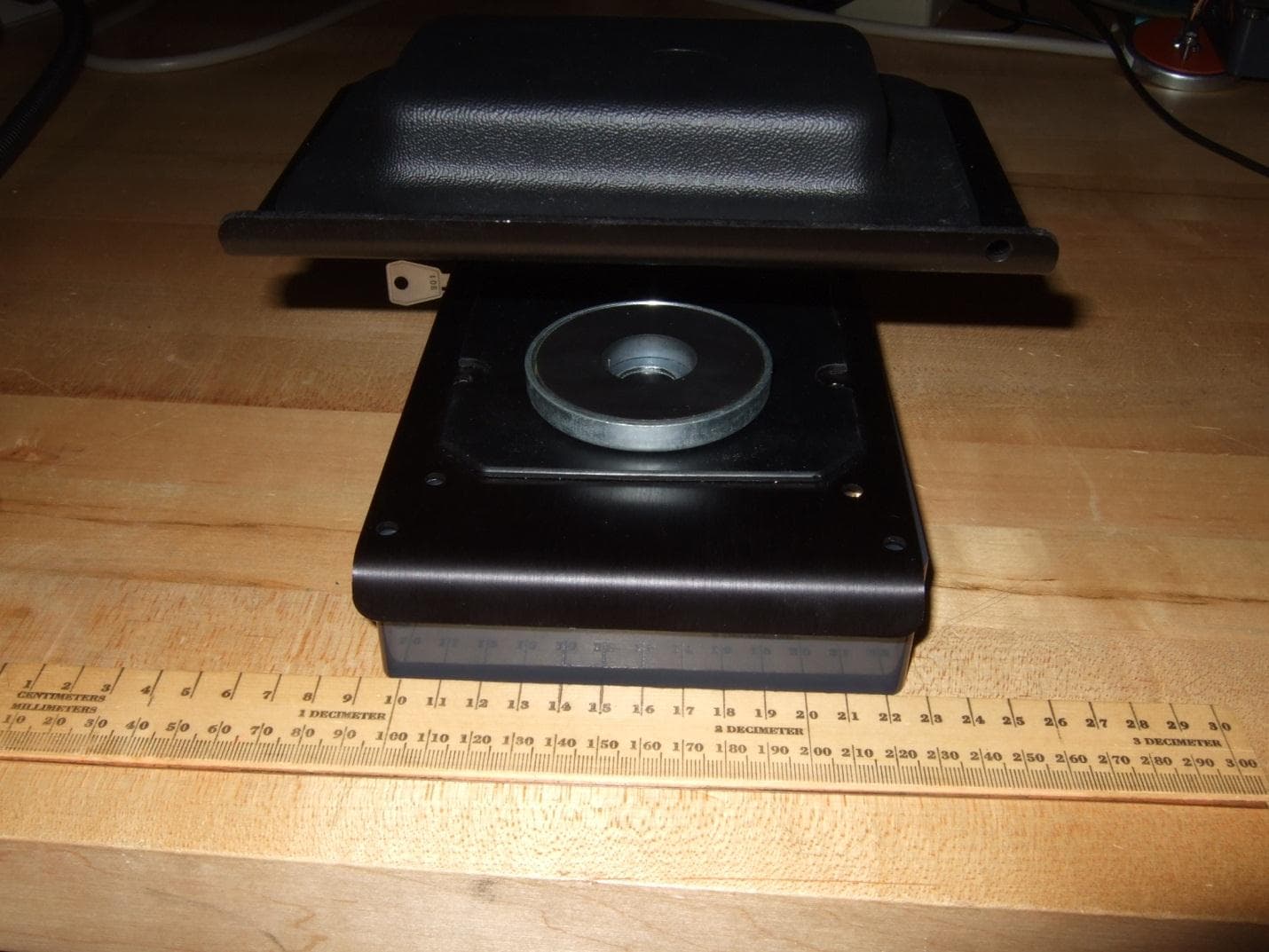
XDY-VERSA-01
Apr 04, 2013GPS based tracking device with GSM and Globalstar modules
Equipment Class
DTS - Digital Transmission System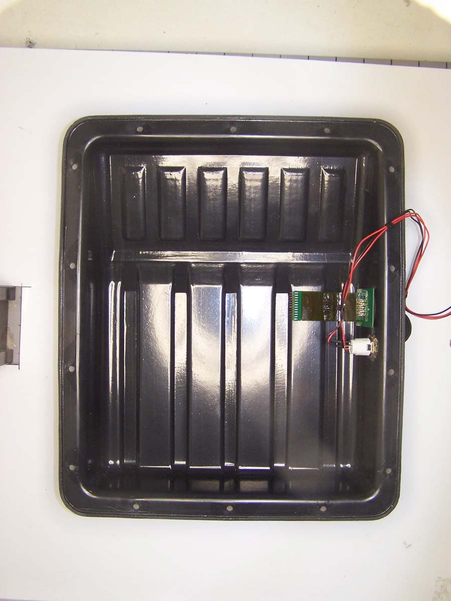
XDY-WEDGEV3
Jun 27, 2010local control for remote installation
Equipment Class
DTS - Digital Transmission System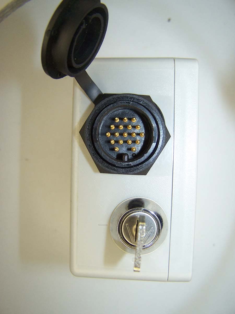
XDY-GTLITEV3
Jun 27, 2010local control for remote installations
Equipment Class
DTS - Digital Transmission System