XJN-PX7052Mobile Internet Device
SHUOYING INDUSTRIAL (SHENZHEN) CO., LTD.
Click to zoom
Application Details
- Equipment Class
- DTS - Digital Transmission System
- Date of Grant
- Jan 26, 2014
- Application Purpose
- Original Equipment
- Date of Application
- Jan 26, 2014
- Equipment Note
- Mobile Internet Device
- Frequency Range
- 2422.00000000 - 2452.00000000
- Country
- China
Documents & Files
Document Text
Text extracted from the exhibit documents filed with the FCC. Open a document above to read the original.
Users Manual
1 Attention: This handbook contains important security measures and the correct use of the product information, in order to avoid accidents. Please make sure to reading the manual carefully before use the device. z Please don’t be in high temperature, moisture or very dust place z Please don’t be in high temperature, especially in summer don't put the device in the car when Windows closed. z Avoid fall or Violent collision of the device, don’t make the TFT display screen were violent tremor, This could cause TFT display screen abnormal or damage. z Please choose the appropriate volume, Use headphones should not be too big volume, If feel tinnitus, Lower the volume or stop using it z please charge In the following condition, A 、 The battery power ICONS shows have no power B 、 The system automatically shut off, startup after power off soon C 、 Operation buttons no response D 、 The machine that the top right corner show red icons z When the device in the format or ongoing upload and download file, please don't suddenly disconnect, This could cause application error. z For those who because of damage to the product, repair, or other causes of erased the memory, The company shall not be liable for any responsibility, please follow the user manual for the standardized operation to use the device. z Don’t disassemble the product, don’t use alcohol 、 Thinner or benzene to scrubbing products z Don't use the device one of the place of prohibit to use electronic equipment in regional (such as the plane) 2z Please don't using the Tablet PC when you in driving or walking down the street, z USB just only be used for data transmission The company reserves the right to improve product, products specification and design have any change, The information is subject to changes without prior notice. (This tablet is no waterproof function) 【 Remark 】 All pictures in this manual is just for your reference. products specification and design have any change, The information is subject to changes without prior notice. 31 . Appearance and button: Front View: Rear View: (1) Camera (2) MIC (3) Power (4) Earphone jack (5) Micro USB (6) Charging interface (7)HDMI (8) TF card (9) Reset (10) Speaker 41.1 Touch panel 7” Capacitive touch panel: In the Operation, to click, dragging on the touch panel. 1.2 POWER startup: Long Press and hold the power button, the system will enter the main interface. shutdown: In the main menu interface, Press the power button about 5 second to shutdown, The system can hint "power off" option, Click ”ok”. You can safely shut down. Lock screen: Short press Power button to lock screen or unlock screen. Remark 1.When power is empty, system will shut down automatically. 2. Illegal turn off the device, restart will scan and restore the disk, it may take longer time to enter into system. 1.3 Reset When tablet PC has failure, press the reset hole (R) with a sharp object, and the tablet PC will be turned off. [Remark]: Unless necessary, do not press the reset button. 1.4 HDMI The port connect with TV and show HDMI file. 1.5 earphone jack 3.5 mm standard earphone jack 1.6 Micro SD card Micro SD card slot: external Micro SD card. 1.7 Micro USB Micro USB jack: you can use it to connect the computer for data transmission, charging and external connection USB flash drive. 52. First use 2.1 Battery management and charge Before first use, please set the device's battery is fully charged Just need to connect the adaptor or USB interface, then you can charge The first two times charging please keep about 6 hours, after that you just need 4 hours to charge. 【 Remark 】 : This tablet using Built-in type polymer battery, Charge must be to choose standard adaptor (Input: AC110~240V 50/60Hz Max : 180MA.. Output: DC5.0~5.5V/1.5A), this device without supply DC charging, USB interface can charge, Choose USB interface to charger During the charging, the battery icon will scroll When finished charging, battery icon will become green and stop rolling In order to prolong the service life of the machine, suggest use out battery power before charge it 【 Remark 】 : 1. If you long time doesn’t to use this Tablet, in order to avoid power consumption caused damage, please charge/play the battery once a month. 2 、 After low battery shut down, connect DC adaptor, device will remind low battery, charging, need to wait some time until the battery is enough power to enter into main menu. 3. Device charging should be in standby status for reach normal charging time. Because with device and screen consumption, it may cause longer charging time. 62.2 Connection with PC Use USB cable to connect device to PC, device will pop up the USB connection window, click Turn on USB storage to connect to PC. Into the load mode, you can copy; delete the file on the device and the file on the memory card. 3. Equipment operation interface 3.1 Unlock Interface After starting up, the Locking interface will be shown firstly, just as the following: It is only available to conduct operation after unlocking. Unlocking method: touch the right Lock icon by hands, and drag it next to a lock at the right, then release hands. The system will be unlocked, and enter the main interface. If drag it to the left, the system will enter the Camera mode. 73.2 Main interface describe The main interface of the handheld tablet includes two modes: the small tools on the desktop mode and the icons of application programs mode, both of which can be switched between each other via the button at the top right corner. The mode of small tools on the desktop is shown as follows: Ta p button on the shortcut bar to enter the interface of icon modes for application programs, which is shown as follows: 8 Tap button to enter the desktop interface. 93.3 Shortcut Mode Under the interface of the mode of small tools on the desktop, after pressing Menu key, the Shortcut menu will popup at the bottom of the screen, shown as follows: 3.4 Usage of Small Tools on Desktop Users can add, delete …
Text truncated - open the document above for the full version.
Block Diagram
55 44 33 22 11 D D C C B B A A I2C USB OTG IMAPX15 I2S Interface Camera Interface DDR Memory Infotmic SD/TF Interface HDMI Interface amplifier ES8328E Audio codec WIFI DDR2/3 Interface Gsensor NAND Flash RGB LCD LCD_RGB USB HOST NAND Flash Interface
External Photos
EXHIBIT B - EUT EXTERNAL PHOTOGRAPHS EUT—All View EUT—Top View EUT—Bottom View EUT- Port Side View EUT- Right Side View EUT— Left Side View EUT—Adapter View EUT—Adapter Label View
ID Label/Location Info
EXHIBIT A - FCC ID LABELING AND LOCATION FCC ID Label Proposed FCC ID Label Location The label shown shall be permanently affixed at a conspicuous location on the device and be readily visible to the user at the time purchase (Labeling requirements per 2.925) Label Here
Internal Photos
EXHIBIT B - EUT EXTERNAL PHOTOGRAPHS EUT- Uncover View EUT- Shielding Off View Antenna EUT-Main Board Off View EUT-Main Board Top View EUT-Main Board Bottom View EUT- RF Module View EUT- Antenna View EUT- Battery Top View EUT- Battery Bottom View EUT- Screen Display Top View EUT- Screen Display Bottom View
Operational Description
Product Diagram Information 1. Product function introduce PX7052 is an Android MID device with capacitive touch screen. It have functions of visiting internet with WiFi, playing audio and video in NAND flash or TF card, audio/video recorder, alarm clock, calendar, real-time clock, camera and so on. 2. Structure 2.1 Structure Introduce The system is consist of SOC(X15,Infotmic),one piece of NAND Flash, 2 pieces of DDR3 RAM, 7” TFT panel, WiFi module (7601), TF socket, 30W front camera (SP0838) , PMU (AXP202), and some other power conversions IC. 2.2 Description When you stir the switch of power about 3 seconds, the system is powered on. When you choose any icon in the GUI of Android 4.1 using your finger or others, X15 first judge what happened and then give it to the ARM or DSP in the core of X15 proceeding. WIFI Module Frequency Range: 2412-2462MHz for 802.11b/g/n; Modulation: OFDM with BPSK/QPSK/16QAM/64QAM for 802.11g/n, DSSS with DBPSK/DQPSK/CCK for 802.11b Type of Antenna: PCB antenna Antenna Gain: 2dBi 2.3 Power It can use adaptor of 5V*2A when the system display the battery remain a little of power or exhaust.
Schematics
55 44 33 22 11 D D C C B B A A AXP202 Trace width should greater than 60milTrace width should greater than 30milTrace width should greater than 15mil (MAX)1.2A 3.3V(MAX)1.6A 1.2V Core Power supply 1.2V RTC Power Power Key Charge STA: L-->Empty H-->Full Power_EN: L-->OFF H-->ON Reset-key RTC Circuit STAT STAT I2C_SCL0I2C_SDA0 BAT CORE_POWER_EN CORE_POWER_EN POWER_KEY I2C_SCL0I2C_SDA0 32K_CLK_OUT Alarm_Wakeup_INT AUTO_BOOTAlarm_Wakeup_INTCTP_POWER_EN CTP_POWER_EN AUTO_BOOT 32K_CLK_OUT VDDIO33 ACIN5V VCCAU33 CAMAVDD28 CAMDVDD18 V_BAT V_BAT V_BAT VDDRTC33 USBVBS V_BAT VDDRTC33 VDDRTC11 VDDPLL25 V_BAT V_BAT VDDIO33 VDDRTC33 VDDRTC33 VDDC_CPU VDD_DDR3 VDDC_CPU V_BAT V_BAT USBVBS ACIN5V Charge_STA I2C_SDA0I2C_SCL0 PMU_IRQ_INT DRVBUS 32K_CLK_OUT Core_V_PWM CTP_POWER_EN SYS_RESET C1622.2uF/10VC0402 U22 PCF8563TS TSOP8-0D5-3X3MM OSCI 1 OSCO 2 INT 3 VSS 4 SDA 5 SCL 6 CLKOUT 7 VDD 8 C1141uF/25VC0402 SW2 BUTTON_SW SWRE 13 42 R16310KC0402 C1571uF/25VC0402 C11710uF/6.3VC0805 C15510uF/6.3VC0805 C1454.7uF/10VC0402 R17510KC0402 C1602.2uF/10VC0402 R?10KR0402 C155 10uF/6.3V C0402 R152 0.030R/F C0402 U18XC6206M-12SOT-23 VIN 3 GND 1 VOUT0 2 C1592.2uF/10VC0402 TP130TP30 C120 22pF/50VC0402 C1151uF/25VC0402 R178 1K R0402 C154 1uF/25V C0402 C1612.2uF/10VC0402 C14710uF/6.3VC0402 R138100K 1%C0402 R1771RC0402 C1634.7uF/10VC0402 C1514.7uF/10VC0402 TP131TP30 V5NC/ESD9B5VTVS0402 TP124TP30 + C12210uF/6.3VC0805 L12 2.2uH/3A CD43 TP128TP30 L11 2.2uH/3A CD43 C16710uF/6.3VC0805 X3 32.768KHz xtal-crystal-ms3v-t1r R186NC/10K_1%R0402 SW1 BUTTON_SW-A VOLUME_4P 2 1 4 3 J8DC_JACK SMD_DC_A245_5P_PL_A GND 3 DC 1 G1 2 GND2 4 GND1 5 D12NC/BLUE-LED C0402 R159200K 1%C0402 C15622pF/50VC0402 TP125TP30 U20 SY8009B sot23-6 EN1 1 GND 2 LX 3 VIN 4 NC 5 FB 6 C1464.7uF/10VC0402 R162 1.5KC0402 L10 2.2uH/2A CD43 C15310uF/6.3VC0402 C15722pF/50VC0402 R?100KR0402 R187 NC/10K_1% R0402 R?100KR0402 C150 10uF/6.3V C0402 TP102TP30 R15510KR0402 R188NC/10K_1%R0402 C121 0.1uF/50VC0402 C14410uF/6.3VC0402 TP126TP30 C1581uF/25VC0402 R157100KR0402 C149 10uF/6.3V C0402 R135 150K 1% C0402 R185 NC/270K_1% R0402 C159 NC/0.1uF/50VC0402 L13 2.2uH/3A CD43 C1581uF/25VC0402 C148 10uF/6.3V C0402 U23 AXP202S-PVQFN-N48-P0_4 SDA 1 SCK 2 GPIO3 3 N_OE 4 GPIO2 5 N_VBUS_EN 6 VIN2 7 LX2 8 PGND2 9 DCDC2 10 LDO4_OUT 11 LDO2_OUT 12 LDO2_4_VIN 13 VIN3 14 LX3 15 PGND3 16 DCDC3 17 GPIO1 18 GPIO0 19 EXT_EN 20 APS 21 AGND 22 BIAS 23 VREF 24 PWROK 25 VINT 26 PWREN 27 LDO1_OUT 28 DC3SET 29 BACKUP 30 VBUS_IN 31 AC_IN1 32 AC_IN2 33 IPSOUT1 34 IPSOUT2 35 CHGLED 36 TS 37 BAT1 38 BAT2 39 LDO3_IN 40 LDO3_OUT 41 BATSENSE 42 CHSENSE 43 VIN1 44 LX1 45 PGND1 46 PWRON 47 IRQ/WAKEUP 48 GND_THE 49 C1180.1uF/50VC0402 R178 20K R0402 C1564.7uF/10VC0402 TP129TP30 C143 1uF/25V C0402 J5BAT BAT-PMP 12 V4NC/ESD9B5VTVS0402 R204 0 R0402 TP127TP30 R17930KR0402 55 44 33 22 11 D D C C B B A A EarPhone Speaker Audio codec ES8323 Amplifier 1.If use ES8328,Pls add C133 and C135,R94.will be remove R91,R92 and R93.2.If use ES8323 ,Pls add R91,R92 and R93,will be remove C133,C135 and R94. If use LM4890,pls change R194 Value for 0, other value Pls reference amplifier application I2C_SDA1_AUI2C_SCL1_AU I2C_SCL1I2C_SDA1 I2C_SCL1_AUI2C_SDA1_AU AGND ROUTLOUT SPKR+SPKR- MUTE ADC_VREF MIC_P MIC_PMIC_N MIC_N AU_SDOAU_MCLKAU_SDIAU_BCLKAU_SYNC ADC_VREF LOUTROUTAGND ROUTLOUT VCCAU33 VCCAU33 VBAT VCCAU33 VCCAU33 I2C_SCL1I2C_SDA1 JACK_DET SPK_MUTE AU_MCLKAU_SDOAU_BCLKAU_SDIAU_SYNC C820.1uF/50VC0402 V1ESD9B5V/NC TVS0402 C1320.1uF/50V C0402 U10 LM4890 MSOP8 SHUT 1 Vref 2 +IN 3 -IN 4 Vo- 5 VDD 6 GND 7 Vo+ 8 C1304.7uF/10VC0603 R195 5.1K_1% R0402 R178 NC/10KR0402 R94 10K R0402 V3ESD9B5V/NC TVS0402 R194 0R R0402 U22 ES8323DS ES8323-QFN28 DVDD 2 PVDD 3 DGND 4 MCLK 1 SCLK 5 DSDIN 6 DLRCK 7 ASDOUT 8 NC4 9 CE 26 SCL 28 SDA 27 NC2 24 NC1 23 LIN1 22 RIN1 21 VREF 10 HPVDD 16 AVDD 17 AGND 18 HPGND 13 NC7 12 NC6 11 LOUT1 15 ROUT1 14 NC3 25 ADCVREF 19 VMID 20 GND_THER 29 R150 330R R0402 R96 10K R0402 V2ESD9B5V/NC TVS0402 R17910KR0402 R149 NC/0R R0402 R14547RR0402 R931KR0402 C1284.7uF/10VC0603 TP133TP30 C166NC/0.1uF/50VC0402 R92 43K R0402 C141 100pF/50VC0402 R151 330R R0402 C1402.2uF/10VC0402 C136 0.1uF/50V C0402 R14647RR0402 R88 10K R0402 + C88 10uF/6.3V C0805 1 2 TP134TP30 C1392.2uF/10VC0402 R202 NC/10K R0402 C84 0.47uF/50V C0402 C1372.2uF/10VC0402 R1500RR0402 R1482.2KR0402 + C87 10uF/6.3V C0805 1 2 R144 10R R0402 C142100pF/50VC0402 C138 0.1uF/50V C0402 MIC1 MIC MIC-WM-64PC 21 C148 4.7uF/10V C0603 J2Speaker-R/NC SPK_2PIN 12 R91 10K R0402 R19610KR0402 R1492.2KR0402 R8930KR0402 C814.7uF/10VC0603 J9 Audio_JACKpj-311-6b 145632 55 44 33 22 11 D D C C B B A A OTG/HOST/Charger Trace width should greater than 70mil DRVBUS: L-->OFF H-->ON Input Current limit: Iimit(A)=6800/Rset USBVBS VBAT VDDIO33 VDD5V V_BAT USB_OT_ID USB_OT_DMUSB_OT_DP DRVBUS Q15 AO3415 SOT-23 3 1 2 C19610uF/6.3VC0805 R18010K R0402 C10210uF/6.3VC0805 R174 10K R0402 R172 27K1%R0402 Q143904SOT-23 U24 SY7152 SOT23-6 LX 1 GND 2 FB 3 EN 4 IN 5 NC 6 R169100KR0402 L15 4.7uH/3A CD43 R119100K R0402 R171 100K R0402 D13 B340 DO-SMA 1 2 C1911uF/25VC0603 R17010KR0402 U15 SY6280A SOT23-5 OUT 1 EN 4 GND 2 ISET 3 IN 5 USB MINI CN4 USB/MICUSBUSB_MINI_C VSS 5 VBUS 1 D- 2 D+ 3 ID 4 GND2 6 GND1 7 GND3 8 GND4 9 R173200K1%R0402 C1821uF/25VC0402 C18310uF/6.3VC0805 55 44 33 22 11 D D C C B B A A P_ANT_2G0 P_ANT_2G0_1 RFOUT_G0 RFOUT_G0 [3] ANT [3] GND GND GND GND TitleSize Document Number Rev Date: Sheet of <Doc> <RevCode> <Title> A 11 Saturday, October 27, 2012 TitleSize Document Number Rev Date: Sheet of <Doc> <RevCode> <Title> A 11 Saturday, October 27, 2012 TitleSize Document Number Rev Date: Sheet of <Doc> <RevCode> <Title> A 11 Saturday, October 27, 2012 C2381pFC2381pF L10 1nH L10 1nH 1 2 C240 0.5pF C240 0.5pF C2361pFC2361pF L12 1nH L12 1nH 1 2 C2371pFC2371pF C235 1pF/NI C235 1pF/NI 55 44 33 22 11 E E D D C C B B A A WL_GPIO4 0 : E-fuse1 : EEPROM EE_MISO Boot Strapping (Internal Pull High/Low) 0 : 40MHz Xtal1 : 20MHz Xtal WL_GPIO6 000:Normal Boot from RAM001:Normal Boot from ROMPCI-E ModeUSB Mode010:Norma…
Text truncated - open the document above for the full version.
Test Report
Note: This test report is prepared for the customer shown above and for the device described herein. It may not be duplicated or used in part without prior written consent from Bay Area Compliance Laboratories Corp. This report must not be used by the customer to claim product certification, approval, or endorsement by NVLAP*, or any agency of the Federal Government. * This report may contain data that are not covered by the NVLAP accreditation and shall be marked with an asterisk “★” (Rev.2). This report is valid only with a valid digital signature. The digital signature may be available only under the Adobe software above version 7.0. FCC PART 15.247 TEST REPORT For SHUOYING INDUSTRIAL (SHENZHEN) CO., LTD. NO.1 Shuoying Rd., Hebei Industry Area, Dalang, Longhua Town, Baoan,Shenzhen,China. Report Type: Original Report Product Type: Mobile Internet Devices Test Engineer: Leon Chen Report Number: R2DG131219001-00B Report Date: 2014-01-26 Reviewed By: Ivan Cao RF Leader Test Laboratory: Bay Area Compliance Laboratories Corp. (Dongguan) No.69 Pulongcun, Puxinhu Industrial Zone, Tangxia, Dongguan, Guangdong, China Tel: +86-769-86858888 Fax: +86-769-86858891 www.baclcorp.com.cn FCC ID: XJN-PX7052 Bay Area Compliance Laboratories Corp. (Dongguan) Report No.: R2DG131219001-00B FCC Part 15.247 Page 2 of 63 TABLE OF CONTENTS GENERAL INFORMATION.......................................................................................................................................4 PRODUCT DESCRIPTION FOR EQUIPMENT UNDER TEST (EUT) .....................................................................................4 OBJECTIVE...................................................................................................................................................................4 RELATED SUBMITTAL(S)/GRANT(S).............................................................................................................................4 TEST METHODOLOGY..................................................................................................................................................4 TEST FACILITY.............................................................................................................................................................5 SYSTEM TEST CONFIGURATION ..........................................................................................................................6 DESCRIPTION OF TEST CONFIGURATION......................................................................................................................6 EUT EXERCISE SOFTWARE..........................................................................................................................................6 SUPPORT EQUIPMENT LIST AND DETAILS....................................................................................................................7 EXTERNAL I/O CABLE..................................................................................................................................................7 BLOCK DIAGRAM OF TEST SETUP................................................................................................................................7 SUMMARY OF TEST RESULTS...............................................................................................................................8 FCC §15.247 (i) & §1.1310 & §2.1093- RF EXPOSURE ...............................................................................................9 APPLICABLE STANDARD..............................................................................................................................................9 FCC §15.203 - ANTENNA REQUIREMENT...........................................................................................................10 APPLICABLE STANDARD............................................................................................................................................10 ANTENNA CONNECTOR CONSTRUCTION....................................................................................................................10 FCC §15.207 (a) – AC LINE CONDUCTED EMISSIONS .....................................................................................11 APPLICABLE STANDARD............................................................................................................................................11 MEASUREMENT UNCERTAINTY..................................................................................................................................11 EUT SETUP................................................................................................................................................................11 EMI TEST RECEIVER SETUP.......................................................................................................................................12 TEST PROCEDURE......................................................................................................................................................12 CORRECTED AMPLITUDE & MARGIN CALCULATION.................................................................................................12 TEST EQUIPMENT LIST AND DETAILS.........................................................................................................................13 TEST RESULTS SUMMARY..........................................................................................................................................13 TEST DATA................................................................................................................................................................13 FCC §15.209, §15.205 & §15.247(d) - SPURIOUS EMISSIONS.............................................................................16 APPLICABLE STANDARD...................................................................................................................…
Text truncated - open the document above for the full version.
Test Setup Photos
EXHIBIT D - TEST SETUP PHOTOGRAPHS Conducted Emissions - Front View Conducted Emissions – Side View Radiated Emission -Front View (Below 1GHz) Radiated Emission - Rear View (Below 1GHz) Radiated Emission -Front View (Above 1GHz) Radiated Emission - Rear View (Above 1GHz)
Contact Information
Applicant
Tony Pan
Test Firm
Bay Area Compliance Laboratories Corp. (Dongguan)John Chan
[email protected]86-769-86858888
Technical Specifications
| # | Rule Parts | Frequency Range | Power Output |
|---|---|---|---|
| 2 | 15C | 2.42 GHz - 2.45 GHz | 8.02 mW |
Other Applications from SHUOYING INDUSTRIAL (SHENZHEN) CO., LTD.
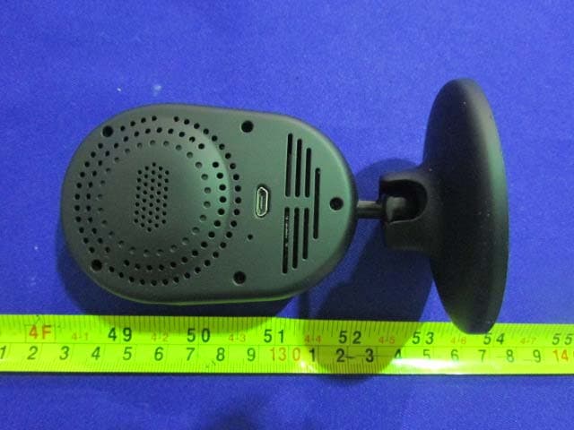
XJN-IPC019
Sep 07, 2015IP Camera
Equipment Class
DTS - Digital Transmission System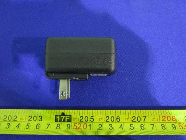
XJN-PA7062X
Dec 27, 2014Mobile Internet Devices
Equipment Class
JBP - Part 15 Class B Computing Device PeripheralXJN-PX4032
Sep 20, 2014Mobile internet device
Equipment Class
DTS - Digital Transmission System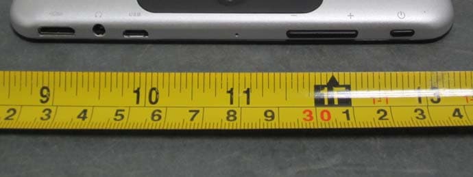
XJN-PA7810X
Jun 26, 2014Mobile Internet Devices
Equipment Class
DSS - Part 15 Spread Spectrum Transmitter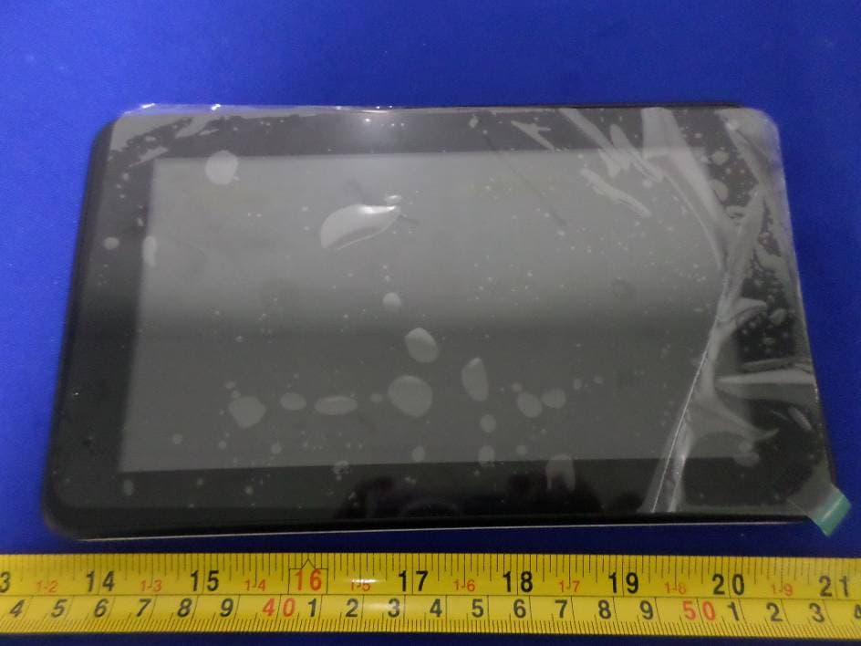
XJN-PR7062X
May 06, 2014Mobile Internet Device
Equipment Class
DTS - Digital Transmission System