XRH-1997WIRELESS WLAN MODULE
North Pole Engineering, Inc.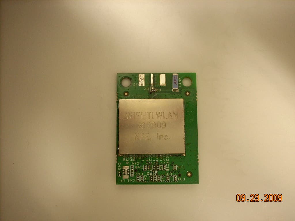
Click to zoom
Application Details
- Equipment Class
- DXX - Part 15 Low Power Communication Device Transmitter
- Date of Grant
- Apr 17, 2010
- Application Purpose
- Original Equipment
- Date of Application
- Apr 17, 2010
- Equipment Note
- WIRELESS WLAN MODULE
- Frequency Range
- 2402.00000000 - 2462.00000000
- Company
- North Pole Engineering, Inc.
- Country
- United States
Documents & Files
Document Text
Text extracted from the exhibit documents filed with the FCC. Open a document above to read the original.
Users Manual
WiFi-IT!™ WLAN Module www.npe-inc.com Page 1 of 16 ©2009 by NPE, Inc. v1.3 WL10-G - 3/19/2010 WL10-G WiFi-IT! KEY FEATURES Battery Operation (7.5 μA Sleep Current) Small Form Factor (1.3” x 1.8”) Timer and Event Triggered Auto-reporting Capability Analog, Digital, Serial and PWM Interfaces Multiple Active Interfaces Real-Time Clock Security: WEP128, WPA-PSK and WPA2-PSK (TKIP / AES) Simple Wireless-Wire Mode WLAN Stack Built-in UART Interfaces Support Hardware Flow Control -40 to +85 °C Operating Temperature Range 2.0 volts to 3.3 volts Operating Voltage 802.11b/g Wireless Network Module GENERAL INFORMATION The WiFi-IT wireless module is a low cost, easy to integrate, robust solution for providing low to mid-speed WLAN communication. WiFi-IT is perfectly suited for creating sensor- based networks that require no additional programming. The module supports a wide range of interfaces including, UART, SPI (master and slave), I2C, Digital, Analog and Pulse Width Modulated (PWM). Multiple active interfaces are supported! WiFi-IT is compatible with standard 802.11 b/g wireless access points. MODULE BLOCK DIAGRAM 802.11 b/g Transceiver & Processor Balun Alarm 0Alarm 1 VDD 3.3v 1.8v VDD_ADC VDD_IO SPI 0/GPIO SPI 1/GPIO UART 0/GPIO UART 1/GPIO I2C/GPIO PWM 0 ADC 0 / DAC ADC 1 PWM 1 PWM 2 GPIO Ready 44 MHz 32 Khz WiFi-IT!™ WLAN Module www.npe-inc.com Page 2 of 16 ©2009 by NPE, Inc. v1.3 WL10-G - 3/19/2010 WL10-G HARDWARE DESCRIPTION The WiFi-IT module operates in the 2.4 GHz ISM band and supports two standard 802.11 b/g data rates, 1 Mb/s and 2 Mb/s. The module provides a variety of hardware interfaces that may be active at any time. There are two UARTs, each providing an asynchronous communication interface supporting all standard bit rates up to 921.6 kbps. Both UARTs support hardware flow control, if enabled. Two SPI interfaces provide dual synchronous serial communication and operate in either slave or master modes. SPI 0, when configured as a master device, provides up to four chip selects. One I 2 C port is provided supporting bit rates of up to 392 kbps. Three Pulse-Width Modulation (PWM) outputs are provided. The PWM outputs operate in two modes; as independent function blocks providing an output signal with programmable frequency and duty cycle, or as synchronized PWM function blocks with programmable phase delay between each PWM output. Two ADC inputs provide 10-bit A-to-D conversions at up to 32 ksps. ADC 0 can be configured as a DAC providing 10-bit D-to-A conversions. When ADC 0 is used as a DAC, ADC 1 is disabled and should be left unconnected. Unused pins are available as General Purpose I/O (GPIO), which may be programmed as Input (default), Output or Bi-Directional. Two Alarm inputs are provided to wake the WiFi-IT from the power conservation sleep mode. The Alarm inputs have programmable polarity and are Schmidt-triggered logic. The Ready output goes active when the module is ready to communicate. FIRMWARE DESCRIPTION The WiFi-IT module is available preloaded in two different configurations. The Wireless-Wire (L1) configuration requires no programming, just use the configuration application to setup your desired operation parameters. The WiFi-IT Basic (L2) application provides a Basic language interpreter, enabling the engineer to design, code and debug their own applications. Using the WiFi-IT! Module and WiFi-IT Basic you can replace the microprocessor in many embedded designs! WIFI-IT! WIRELESS-WIRE The Wireless-Wire application supports configuration of a nodes interface ports and control engine. It is also used to setup the wireless communication parameters either remotely or through an RS232/USB port on a Personal Computer. Interface ports can be enabled and configured with the desired operating parameters. The node control engine can me setup to operate in three unique modes: 1. Sleeping sensor node with timer or interrupt auto-reporting. 2. Sleeping data node with timer or interrupt auto-reporting. 3. Always-on node with interrupt, timer or continuous connection. Once configured the WiFi-IT node permanently stores the settings and will operate, using those settings, until they are changed. The Wireless-Wire Configuration application can update node operating parameters over the wireless network at anytime. WiFi-IT!™ WLAN Module www.npe-inc.com Page 3 of 16 ©2009 by NPE, Inc. v1.3 WL10-G - 3/19/2010 WL10-G The Wireless-Wire protocol supports UDP communication between the node and an Access Point. Communication between a Microsoft Windows® PC and the WiFi-IT nodes is directly supported through a supplied virtual COM port (vCOM) driver. Once the vCOM port is created the connection to the embedded system containing the WiFi-IT node operates just as a wired connection. Data can be transferred from the embedded system or sent to the embedded system through the vCOM port. When operating with legacy RS232 equipment, no modifications to the legacy communication protocol need to be made, in many instances. The Wireless-Wire wraps the legacy communication messages in its own protocol for transmission and removes the wrapper before forwarding the communication on to the legacy system. ` Wireless-Wire Configuration WiFi-IT! Control Software & vCOM Figure 1: L1 System When operating in one of the sleep modes there may be a latency period until the node leaves the sleeping state and connects to the WLAN. The vCOM port can be configured to buffer messages until the node is available. WIFI-IT BASIC (L2) APPLICATION The WiFi-IT Basic application provides a higher level of control requiring programming to implement a solution. Using the WiFi-IT development environment with WiFi-IT Basic, sophisticated programs can be written providing direct program control of an embedded system. WiFi-IT Basic provides a simplified Application Programming Interface (API) to the WLAN, special sleep modes and control of the hardware interfaces. The WiFi-IT development environment provides tools to debug the a…
Text truncated - open the document above for the full version.
Block Diagram
North Pole Engineering, Inc. WiFi IT WLAN Module Model: WL10-GC, GS Block Diagram
Cover Letter(s)
1100 Falcon Ave. Tele:320-864-4444 Glencoe, MN 55336 Fax: 320-864-6611 “Your Agent to Product Certifications and Licenses Throughout the World” To: TIMCO March 19, 2010 From: Duane R. Bagdons Cover Letter for request for a Limited Single Modular Approval FCC ID: XRH-1997 This request is for a Single Modular Approval. This unit is a module that operates in the 2400 to 2483.5 Mhz frequency band. The above FCC ID product is a plug in module board that is plugged in as a daughter board to the Main host board and provides wireless communications in the 2400 to 2483.5 Mhz frequency band. • (i) “The radio elements of the modular transmitter must have their own shielding. The physical crystal and tuning capacitors may be located external to the shielded radio elements.” This EUT (FCC ID: XRH-1997) Has its own shielding of the radio elements • (ii) “The modular transmitter must have buffered modulation/data inputs (if such inputs are provided) to ensure that the module will comply with Part 15 requirements under conditions of excessive data rates by over-modulation.” The processor chip in this module is a Gainspan GS1010WiFi ultra low power wireless single chip The control of the output data stream is controlled by the internal firmware and logic design in this chip to prevent excessive data rates by over modulation. • (iii) The Modular transmitter must have its own power supply regulation. A linear voltage regulator (NCP700MN180R2G) is provided on the modular board to provide power to the Gainspan chip. • (iv)The modular transmitter must comply with the antenna and transmission system requirements of Sections 15.203, 15.204 (b) and 15.204 (c). The antenna must either be permanently attached or employ a “unique” antenna coupler (at all connections between the module and the antenna, including the cable). The “professional installation” provision of Section 15.203 is not applicable to modules but can apply to limited modular approvals under paragraph (b) of this section. Two antennas were tested with this EUT. (1) is a Chip antenna (PC Board mount) Antenna Facdtor, Inc. Model: ANT-2.45-CHP-x that has a gain of 0.5 dBi and (2) an external antenna made by Taoglas Model: GW.11.A153 which has a maximum gain of +1.8 dBi. There are no adjustments on the EUT. • (v) The modular transmitter must be tested in a stand-alone configuration, i.e., the module must not be inside another device during testing for compliance with Part 15 requirements. Unless the transmitter module will be battery powered, it must comply with the AC line conducted requirements found in Section 15.207. AC or DC power lines and data input/output lines connected to the module must not contain ferrites, unless they will be marketed with the module (see Section 15.27 (a)). The length of these lines shall be the length typical of actual use or, if that length is unknown, at least 10 centimeters to insure that there is no coupling between the case of the module and supporting equipment. Any accessories, peripherals, or support equipment connected to the module during testing shall be unmodified and commercially available (see Section 15.31 (i). INTERNATIONAL CERTIFICATION SERVICES INC. International Certification Services, Inc. [email protected] This module was tested in a stand-alone configuration. It was plugged into the Host development board and was tested outside the Host box. The EUT is normally plugged into a header connector on the Main PC board in the HOST so there normally is no cable assembly used to plug in the EUT. The EUT is not battery powered hence the conducted emissions test was performed on the Host box. These photos are shown in the test report. • (vi) The modular transmitter must be equipped with either a permanently affixed label or must be capable of electronically displaying its FCC identification number. • (vi)(A) If using a permanently affixed label, the modular transmitter must be labeled with its own FCC identification number, and, if the FCC identification number is not visible when the module is installed inside another device, then the outside of the device into which the module is installed must also display a label referring to the enclosed module. This exterior label can use working such as the following: “Contains Transmitter Module FCC ID: XYZMODEL1” or “Contains FCC ID: XYZMODEL1.” Any similar wording that expresses the same meaning may be used. The Grantee may either provide such a label, an example of which must be included in the application for equipment authorization, or, must provide adequate instructions along with the module which explain this requirement. In the latter case, a copy of these instructions must be included in the application for equipment authorization. The module has a permanently affixed label on the pc board . The Host also has a label on the outside of the chassis declaring that it contains the above FCC ID product. Photos of this are included in the filing attachments. • (vii) The modular transmitter must comply with any specific rules or operating requirements that ordinarily apply to a complete transmitter and the manufacturer must provide adequate instructions along with the module to explain any such requirements. A copy of these instructions must be included in the application for equipment authorization. All the requirements of FCC 15.249 are met and the manufacturer has provided installation instructions for this module (this is an attachment the filing of this device).
External Photos
North Pole Engineering, Inc. WiFi IT WLAN Module Model: WL10-GC PC Board Component side Chip Antenna SMA connector location for external antenna North Pole Engineering, Inc. WiFi IT WLAN Module Model: WL10-GC PC Board Solder side
ID Label/Location Info
North Pole Engineering, Inc. WiFi IT WLAN Module Model: WL10-GC Module Label Photo
Internal Photos
North Pole Engineering, Inc. WiFi IT WLAN Module Model: WL10-GC PC Board Component side Chip Antenna SMA connector location for external antenna North Pole Engineering, Inc. WiFi IT WLAN Module Model: WL10-GC PC Board Solder side
Internal Photos
North Pole Engineering, Inc. WiFi IT WLAN Module Model: WL10-GC Module with shield removed Photo
Operational Description
North Pole Engineering, Inc. WiFi IT WLAN Module Model: WL10-GC Operational Description The WiFi-IT module is made up of two main subsystems; the Application processor (APP) and the WLAN processor. The WLAN subsystem provides the WLAN PHY, MAC and baseband functionality. It contains the WLAN CPU, a 32-bit ARM7 TDMI-S core running at up to 44 MHz. It includes an IEEE 802.11b/g -compatible RF transceiver, which supports Direct Sequence Spread Spectrum (DSSS) 1 Mb/s and 2 Mb/s data rates. The WLAN sub- system includes an integrated power amplifier, and provides management capabilities for an optional external power amplifier. In addition, it contains engines for AES and RC4 data encryption/decryption, CRC computation, and IEEE1588 precision time protocol network clock synchronization. The WLAN subsystem contains the control logic and state machines required to drive the low power DSSS modem, and perform pre-processing (in transmit mode) or post-processing (in receive mode) of the data stream. The WLAN subsystem manages DMA accesses, data encryption/decryption using the AES algorithm, and CRC computation. The WiFi-IT uses the internal PA to reduce the number of external components required for Wireless LAN connectivity. The internal power amplifier delivers 9 dBm (typical) into a differential balanced 100 ohm load. Its outputs are merged with the LNA inputs through a transistor structure replacing the traditional external TX/RX switch. This solution reduces the off-chip RF BOM to a single low-cost LTCC band pass filter, which also provides differential-to-single-ended conversion. The WiFi-IT App processor runs a program that operates the device interfaces, I2C, UART, SPI, ADC and PWM, to control the attached sensor devices. The data read from the devices can be processed locally and transmitted back to the network through the WLAN processor. The devices connected to the interfaces, are controlled by the code that runs on the APP processor allowing the user to connect a multitude of sensors and provide on-board intelligent decision making capabilities.
Parts List/Tune Up Info
WiFi-IT MC Revised: Thursday, September 24, 2009 WIFITIT001MC Revision: A.05 Bill Of Materials September 24,2009 14:15 :42 Page1 Item Quantity Reference Part Description Footprint Manufacturer Manufacturer Part # Notes 100 Piece Pricing ______________________________________________ 1 1 ANT1 ANT-2.45-CHP-T ANT 2.4GHZ 802.11 BLUETOOTH SMD ANT-245-CHP-X Linx Technologies ANT-2.45-CHP-T DNP 1.33300 2 26 C1,C9,C10,C11,C13,C14, 0.1 uF 0402 10V X5R CAP .10UF 10V CERAMIC X5R 0402 C0402 Kemet C0402C104K8 PACTU 0.01430 C15,C16,C19,C20,C21,C22, C23,C24,C25,C26,C27,C30, C34,C35,C36,C37,C38,C39, C40,C41 3 1 C2 47 pF 0402 250V COG CAP CER 47PF 50V 5% C0G 0402 C0402 Murata GRM1555C1H470JZ01D 0.12412 4 1 C3 47 pF 0402 250V COG CAP CER 47PF 50V 5% C0G 0402 C0402 Murata GRM1555C1H470JZ01D DNP 0.12412 5 3 C4,C7,C8 .01 uF 0402 16V X7R CAP CERM .01UF 10% 16V X7R 0402 C0402 AVX 0402YC103KAT2A 0.03250 6 2 C18,C5 15 pF 0402 50V NPO CAP CERAMIC 15PF 50V NP0 0402 C0402 Kemet C0402C150J5GACTU 0.01430 7 2 C17,C6 22 pF 0402 50V NPO CAP CERAMIC 22PF 50V NP0 0402 C0402 Kemet C0402C220J5GACTU 0.01430 8 1 C12 0.5 pF 0402 50V RFCER CAP CER .5PF 50V 0402 HIGH FREQ C0402 Taiyo Yuden UVK105CH0R5BW-F 0.09750 9 1 C28 22 pF 0402 50V NP0 CAP CERAMIC 22PF 50V NP0 0402 C0402 Kemet C0402C220J5GACTU DNP 0.01430 10 4 C29,C31,C32,C33 1 uF 0402 6.3 V X5R CAP CERM 1 UF 6.3V X5R 0402 C0402 Kemet C0402C105K9PACTU 0.02930 11 2 C43,C42 0.1 uF 0402 10V X5R CAP .10UF 10V CERA MIC X5R 0402 C0402 Kemet C0402C104K8PACTU DNP 0.01430 12 1 C44 .01 uF 0402 16V X7R CAP CERM .01UF 10% 16V X7R 0402 C0402 AVX 0402YC103KAT2A DNP 0.03250 13 1 C45 1 uF 0402 6.3 V X5R CAP CERM 1UF 6.3V X5R 0402 C0402 Kemet C0402C105K9PACTU DNP 0.02930 14 1 J1 544770808 Molex Receptacle 0.4 mm 80 ckt. M OLEX_544770808 Molex 544770808 1.53 15 1 J2 SMA_ANT_CONN CONN JACK END LAUNCH PCB 0.062 " PCB SMA_ANT_CONN1 Emerson Network Power 142-0701 -801 3.33720 16 1 L1 2.2 uH 1000 mA SMT 2.2 uH Power Inductor LP S3015 CoilCraft LPS3015-222MLB 0.66 17 3 L2,L3,L4 0 0805 1/16 1% RES 0.0 OHM 1/8W 5% 08 05 SMD L0805 Yageo RC0805JR-070RL 0.07230 18 1 RFSHIELD1 RFSHIELD RFSHIELD 19 3 R1,R8,R11 10 K 0402 1/10 5% RES 10K OHM 1/10W 5% 0402 SMD R0402 Panasonic - ECG ERJ-2GEJ103X 0.04360 20 4 R2,R3,R4,R5 33 0402 1/10 5% RES 33 OHM 1/10W 5 % 0402 SMD R0402 Panasonic - ECG ERJ-2GEJ330X 0.04360 21 1 R6 0 0402 1/10 5% RES 0.0 OHM 1/16W 0402 SMD R 0402 Stackpole RMCF 1/16S 0 R 0.04360 22 1 R7 10 K 0402 1/10 5% RES 10K OHM 1/10W 5% 0402 SMD R0402 Panasonic - ECG ERJ-2GEJ103X DNP 0.04360 23 1 R9 180K 0402 1/16 1% RES 180K OHM 1/16W 1% 040 2 SMD R0402 Yageo RC0402FR-07180KL DNP 0.02085 24 1 R10 0 0402 1/10 5% RES 0.0 OHM 1/16W 0402 SMD R0402 Stackpole RMCF 1/16S 0 R DNP 0.04360 25 1 U1 GS1010 GainSpan 1010 WiFI SOC QFN-102 GainS pan GS1010 15.00 26 1 U2 DEA252450BT-7012D1 Bandpass filter 2.450 GH z DEA25240BT-8PIN TDK DEA252450BT-7012D1 2.00 27 1 U3 TPS62261DRVT IC STEP-DN CONV 600MA 6-SON SO N2x2-6 Texas Instruments TPS62261DRVT 1.82000 28 1 U4 NCP700MN180R2G IC REG RF LDO 200MA 1.8V 6-D FN DFN-6 ON Semi NCP700MN180R2G DNP 0.72500 29 1 Y1 32.7680KHz FC-135 CRYSTAL 32.7680KHZ 12.5PF SMD FC_135 Epson Toyocom Corporation FC-135 32.768 0KA-A3 1.91250 30 1 Y2 44MHz CRYSTAL 44.000000 MHZ SMD 10PF CRYSTA L_NX2520SA NDK NX2520SA-44.000000MHZ 1.03190
Schematics
55 44 33 22 11 D D C C B B A A A Initial Release MSM 04/16/2009 A.01 Fixed net names for B2_GPIO_13_MSPI_CSC1, B2_GPIO_06_MSPI_DIN A44, B2_GPIO_07_MSPI_DOUT MSM 05/11/2009 Table of Contents Description 23 GS1010 Connector and Power Supply A.02 MSM 05/22/2009 Updated notes on C28, C2, and C3 to reflect actualreference designator after REFD resequencing. A.03 Mirrored symbol and added mounting hole graphics to physically match the 0544770808 connector. MSM 06/15/2009 Page A.04 Changed L2, L3, and L4 to 0 Ohm resistor per GainSpan recommendation change. MSM 07/12/2009 WIFITIT001MC A.04 WiFi-IT MC 1 3 Sunday, July 12, 2009 TitleSize Document Number Rev Date: Sheet of ©2009 North Pole Engineering. This document containsproprietary information and/orintellectual property that is theproperty of North PoleEngineering, Inc. B Reivision History REV Description ENG Date 55 44 33 22 11 D D C C B B A A Connection from this pad to theplane must be beefy! Either bigpower via, or several smallerpower vias. VDD_RTC voltage affects Voh of RTC_DC_DC_CNTL. 50 Ohms 50 Ohms 100 Ohms differential For internal RF amp, B11 connected to V1.8, B12 canalso be connected although it is listed as an NC onthe datasheet, per GainSpan application support. Mutually exclusive population options C2 and C3share one pad. C3 50 Ohms C2 For TPS62260DRVT: R6: 0R7: DNS For TPS62261DRVT: R9: DNS R9: 180K 1%R6: 360K 1%R7: DNS C42: 22pF C42: DNS WIFITIT001MC A.04 WiFi-IT MC 2 3 Sunday, July 12, 2009 TitleSize Document Number Rev Date: Sheet of ©2009 North Pole Engineering. This document containsproprietary information and/orintellectual property that is theproperty of North PoleEngineering, Inc. B B3_GPIO_11_PWM1B3_GPIO_12_PWM2 B6_GPIO_31B6_GPIO_30 B3_GPIO_20_CLKO_22MHzB3_GPIO_19_CLKO_44MHzB3_GPIO_23_PPSB3_GPIO_18_AUXTARGETB3_GPIO_21_CLKO_11MHzB3_GPIO_10_PWM0B3_GPIO_22_CLK_LP RTC_ALARM2RTC_OUT2_LP_CLK_OUTRTC_OUT1RTC_ALARM1 B2_GPIO_07_MSPI_DOUTB2_GPIO_15_MSPI_CSC3B2_GPIO_04_MSPI_CSC0B2_GPIO_06_MSPI_DINB2_GPIO_13_MSPI_CSC1B2_GPIO_14_MSPI_CSC2B2_GPIO_05_MSPI_CLK B1_JTAG_TDI B1_GPIO_29_JTAG_CFG1 B1_JTAG_TMSB1_JTAG_TDO B1_GPIO_28_JTAG_CFG0 B1_JTAG_NTRSTB1_JTAG_TCK ADC2_VREFADC1_DAC B2_EXT_RESETn RTC_DC_DC_CNTL rf_tx_rx_diff_n rf_tx_rx rf_tx_rx_ant2 rf_tx_rx_diff_p rf_tx_rx_ant3 B5_GPIO_27_UART1_RTSB5_GPIO_24_UART0_CTSB5_GPIO_00_UART0_RXB5_GPIO_01_UART0_TX B4_GPIO_09_I2C_CLK B5_GPIO_25_UART0_RTS B4_SSPI_CLKB4_SSPI_DOUTB4_GPIO_08_I2C_DATAB4_SSPI_DINB4_GPIO_16_AUXSNAP0 B5_GPIO_26_UART1_CTSB5_GPIO_02_UART1_TXB5_GPIO_03_UART1_RX B4_GPIO_17_AUXSNAP1B4_SSPI_CS ADC3_GS1011 FLASH_HV_NC B2_RESET_CTRL_TEST RTC_OUT1RTC_OUT2_LP_CLK_OUTRTC_DC_DC_CNTLB2_GPIO_07_MSPI_DOUTB2_GPIO_15_MSPI_CSC3B2_GPIO_14_MSPI_CSC2B2_GPIO_13_MSPI_CSC1B2_GPIO_04_MSPI_CSC0B2_GPIO_05_MSPI_CLK ADC1_DAC B3_GPIO_18_AUXTARGETB3_GPIO_19_CLKO_44MHzB3_GPIO_20_CLKO_22MHzB3_GPIO_21_CLKO_11MHzB3_GPIO_22_CLK_LPB3_GPIO_23_PPSB3_GPIO_12_PWM2B3_GPIO_11_PWM1B3_GPIO_10_PWM0 B6_GPIO_31B6_GPIO_30 B1_JTAG_TDO RTC_ALARM2RTC_ALARM1 B1_JTAG_TCKB1_JTAG_TDIB1_JTAG_TMSB1_JTAG_NTRST B1_GPIO_29_JTAG_CFG1B1_GPIO_28_JTAG_CFG0 B2_GPIO_06_MSPI_DINB2_EXT_RESETn ADC2_VREF B5_GPIO_01_UART0_TXB5_GPIO_26_UART1_CTS B4_SSPI_DIN B5_GPIO_00_UART0_RXB5_GPIO_25_UART0_RTS B4_GPIO_08_I2C_DATAB4_GPIO_16_AUXSNAP0 B5_GPIO_03_UART1_RX B4_SSPI_DOUTB4_SSPI_CSB4_GPIO_09_I2C_CLK B5_GPIO_02_UART1_TX B4_GPIO_17_AUXSNAP1 B5_GPIO_24_UART0_CTS B4_SSPI_CLK B5_GPIO_27_UART1_RTS ADC3_GS1011 1.8VVDD_IO VDD_IO 1.8VVDD_IO VDD_IO 1.8VVDD_IO 1.8V_ADC VDD_RTC 1.8V_RF 1.8V_PLL 1.8V_RF 1.8V_RF 1.8V VDD_IO VDD_IO ANT1 1 Ant POWER Bank 3 PWMGPIO U1CGS1010 A53A54A55A56A57A58A59A60 B20B19 B18 B17B16 GPIO23/PPS GPIO22/CLK_LP GPIO21/CLK_11MHZ GPIO20_CLK_22MHZ GPIO19/CLK_44MHZ PWM2/GPIO12PWM1/GPIO11PWM0/GPIO10 VDDCORE3VDDCORE3 GPIO18/AUXTARGET VDDIO3VDDIO3 R4 33 0402 1/10 5% C20 0.1 uF 0402 10V X5R POWER I2C SPI2 (SLAVE)GPIO/AUXSNAP Bank 4 U1DGS1010 A61A62A63A64A65A66B21 B22B23 B24 B25B26 I2C_CLK/GPIO9 I2C_DATA/GPIO8 SSPI_DOUT SSPI_CLK SSPI_CS SSPI_DIN GPIO17/AUXSNAP1 VDDIO4VDDIO4 GPIO16/AUXSNAP0 VDDCORE2VDDCORE2 R5 33 0402 1/10 5% R11 10 K 0402 1/10 5% C10 0.1 uF 0402 10V X5R C26 0.1 uF 0402 10V X5R C17 22 pF 0402 50V NPO ADC POWER ADCFLASHADC / Flash U1G GS1010 A37A39 A38 A40 ADC1/DAC ADC2/VREF VDD_ADC ADC3_GS1011 C18 15 pF 0402 50V NPO POWER GPIO Bank 6 U1FGS1010 A1 A2 A3 GPIO31 VDDIO6 GPIO30 Bank 1 JTAGGPIO POWER U1A GS1010 A4A5A6A7 A8A9 A10A11A12 GPIO29GPIO28 TCK TDO VDDIO1VDDCORE1 TDI TMS NTRST Y244MHz 2 14 3 C9 0.1 uF 0402 10V X5R C16 0.1 uF 0402 10V X5R J2 SMA_ANT_CONN 1 24 35 C SS SS C22 0.1 uF 0402 10V X5R C27 0.1 uF 0402 10V X5R R10 0 0402 1/10 5% POWER UART0 UART1 Bank 5 U1E GS1010 A67A68A69A70A71A72B27 B28B29 B30 UART1_RTS/GPIO27 UART1_RX/GPIO3 UART1_TX/GPIO2UART0_TX/GPIO1 UART0_RX/GPIO0 UART0_CTS/GPIO24UART1_CTS/GPIO26 VDDIO5VDDIO5 UART0_RTS/GPIO25 C19 0.1 uF 0402 10V X5R C13 0.1 uF 0402 10V X5R C4.01 uF 0402 16V X7R C25 0.1 uF 0402 10V X5R POWER SPI1 (MASTER) MISC Bank 2 U1B GS1010 A41A42 A43 A44A45A46A47 A48 A49 A50 A51A52 TEST EXT_RESETN VDDCORE5 MSPI_DIN/GPIO6 MSPI_CS3/GPIO15MSPI_CS2/GPIO14 MSPI_DOUT/GPIO7 VDDIO2 MSPI_CLK/GPIO5 VDDCORE4 MSPI_CS0/GPIO4 MSPI_CS1/GPIO13 POWER RF TX/RX RF EXT PA CTRL INT/EXT PA PLL XTAL U1I GS1010 A13A14 A15A16 A17A18A19A20 A21 A22A23 A24 A25A26A27A28A29A30 B1B2B3B4B5B6B7B8B9 B10 B11B12 RFRXTXP RFRXTXN VDD_RFRXTXVDD_TX EXTPAPEXTPAP EXTPANEXTPAN VDD_PLL1 VP_VCO_NC PLL_TEST_NC VDD_CP XTALN/EXT_44MHZ XTALP RFSW0RFSW1RFSW2RFSW3 VDD_QUADLOVDD_VCOVDD_VCOVDD_PLL2VDDAVDDAVDD_XOVDD_CODECVDD_CODEC PADAC VDDSWVDDSW C3 47 pF 0402 250V COG GND PAD U1JGS1010 PAD GND U2 DEA252450BT-7012D1 12 3 7 6 5 4 8 NC1 SE V/NC DIF_p NC2 DIF_n GND GND R1 10 K 0402 1/10 5% C2 47 pF 0402 250V COG C120.5 pF 0402 50V RFCER R3 33 0402 1/10 5% C6 22 pF 0402 50V NPO C5 15 pF 0402 50V NPO C11 0.1 uF 0402 10V X5R C24 0.1 uF 0402 10V X5R C7 .01 uF 0402 16V X7R C23 0.1 uF 0402 10V X5R RTC RTC POWER U1H GS1010 A31A32A33A34A35A36B13 B14B15 ALARM1 RTC_OUT1 OSC_32K1/EXT_32KHZ OSC_32K2 DC_DC_CNTL ALARM2 RTC_OUT2/LP_CLK_OUT VDD_RTCVDD_RTC R2 33 04…
Text truncated - open the document above for the full version.
Test Report
TEST REPORT #180909 STANDARD: FCC PART 15 SUBPART C--INTENTIONAL RADIATORS SECTION 15. 249 OPERATION WITHIN THE BANDS 902-928 MHZ, 2400-2483.5 MHZ, AND 5725-5875 MHZ AND 24.0 TO 24.25 GHZ FCC PART 15.212 MODULAR TRANSMITTERS EQUIPMENT TESTED: NORTH POLE ENGINEERING, INC. WIRELESS NETWORK MODULE FCC ID: XRH-1997 MODEL: WL10-GS AND WL10-GC TEST DATE: 18 SEPTEMBER, 2009 INTERNATIONAL CERTIFICATION SERVICES, INC. 1100 Falcon Avenue Glencoe, MN 55336 Tele: 320-864-4444 Fax: 320-864-6611 CERT NO CERT NOCERT NO CERT NO: 2055:01 : 2055:01: 2055:01 : 2055:01 2 of 43 International Certification Services, Inc. Prepared for: Test agent: Test location: Prepared by: . North Pole Engineering, Inc. 221 North 1 st Street, Suite 310 Minneapolis, MN 55401 International Certification Services, Inc. 1100 Falcon Avenue Glencoe, MN 55336 Tele: 320-864-4444 Fax: 320-864-6611 International Certification Services, Inc. 1100 Falcon Avenue Glencoe, MN 55336 Tele: 320-864-4444 Fax: 320-864-6611 International Certification Services, Inc. 1100 Falcon Avenue Glencoe, MN 55336 International Certification Services represents to the client that testing is done in accordance with standard procedures applicable and that reported test results are accurate within generally accepted commercial ranges of accuracy. This report only applies to the specific samples tested under stated test conditions. It is the manufacturer’s responsibility to assure that additional production units of this model are manufactured with identical electrical and mechanical components. International Certification Services shall have no liability for any deductions, inferences or generalizations drawn by the client or others from this report. This report is the confidential property of the client. As a mutual protection to our clients, the public and ourselves, extracts from the test report shall not be reproduced except in full without our written approval. 3 of 43 International Certification Services, Inc. 1.0 TEST SUMMARY TEST REPORT : #180909 COMPANY: AGENT: International Certification Services, Inc. PHONE: 320-864-4444 TEST DATE: EQUIPMENT UNDER TEST: GENERAL TEST SUMMARY: VERIFICATION / CERTIFICATION STATUS: MODIFICATIONS NECESSARY: TESTED BY WRITTEN BY Duane R. Bagdons Duane R. Bagdons North Pole Engineering, Inc. 18 September, 2009 802.11 b/g Wireless Network Module 2.4 Ghz Transmitter Models: WL10-GS and WL10-GC The testing was performed at International Certification Services, Inc. at 1100 Falcon Ave, Glencoe, MN 55336 The 802.11 b/g Wireless Network Module 2.4 Ghz Transmitter Models: WL10-GS and WL10GC was found to be in compliance with the FCC Part 15 Subpart C, Section 15.249 and FCC 15.212 for modular transmitters requirements. None 4 of 43 International Certification Services, Inc. Applicable Standards 47 CFR Ch.1 (07-10-2008 Edition) FCC Part 15 Radio Frequency Devices (July 10, 2008) Subpart C Intentional Radiators Section 15.249 Operation within the bands 902-928 Mhz, 2400- 2483.5 Mhz, 5725-5875 Mhz and 24.0 to 2425 Ghz. Section 15.212 Modular Transmitters 2.1 Referenced Standards ANSI C63.4-2003 Methods of Measurement of Radio-Noise Emissions from Low-Voltage Electrical and Electronic Equipment in the Range of 9 Khz to 40 Ghz. 2.2 Equipment Units Tested The equipment tested was a modular 2.4 Ghz Wireless Network module. This device is a module that takes power from a HOST equipment and post regulates this voltage to the necessary voltages to operate the modular EUT. The Transmitter chip that is used in the design is a Gainspan GS1010 WiFi. There are two antennas that can be configured with this device, one is an external stick type antenna (Taoglas GW.11.A153: Model: WL10-GS) and the other antenna is an internal PC board mounted chip antenna (Antenna Factor ANT- 2.45-CHP-T,B; Model: WL10-GC). The external Stick antenna has a reverse SMA connector as required by FCC 15.203. It can only be configured with one antenna at a time. It is a Digital Modulated Transmitter (DTS) that operates on up to 14 channels in the 2.4 to 2.4835 Ghz frequency band. The transmit time is controlled by the internal firmware of the chip and is compatible with the 802.11 b/g requirements. This module has an on board post regulator to control the voltage to the Intentional Radiator circuitry per the requirements of FCC 15.212 (a) (1) (iii). 2.3 Equipment and Cable Configuration See photo of the EUT test configuration setup in Attachment A 2.4 List of Test Equipment Test Equipment Spectrum Analyzer Harmonic Mixer RF Amplifier Preamp Biconical Antenna Log Periodic Antenna (200-1000 MHz) Horn Antenna (1-18 Ghz) Horn Antenna (18-26 Ghz) Model Hewlett-Packard 8566B Hewlett Packard 11970K Hewlett Packard 11975A Nextec Model: NB00391 EMCO 93110B EMCO 3146 EMCO 3115 Alpha Industries 61932500 S/N 2421A00458 3003A04385 2738A01733 378 105799 9111-3280 2334 55 Calibration Date 01/25/08 10/10/08 09/30/08 06/09/08 06/22/09 01/23/08 06/23/09 01/23/08 5 of 43 International Certification Services, Inc. Measurement cable losses, and antenna correction factors are included in the data sheets. The Resolution BW was set at 1 Mhz and the Video BW was set at 1 Hz with a Span of 0 Hz to perform the correct average detected measurements over 1000 Mhz. 2.5 Units of Measurement. All measurements were taken in dBuV/m with the antenna located at 3 meters distance from the EUT. Frequency measurements are recorded in Mhz 2.6 Location of Test Site The open area test site (OATS) measurement facility used to collect the data was International Certification Services, Inc. at 1100 Falcon Ave in Glencoe, MN 55336. This site has been certified to be in spec of the normalized site attenuation per ANSI C63.4- 2003. (FCC registration number: 640574) 2.7 Measurement Procedures The antenna was placed at a distance of 3 meters from the EUT. The EUT was set on an insulating table in the OATS site and rotated through all orientations to determine the worst case EUT position. The antenna was then positioned…
Text truncated - open the document above for the full version.
Test Setup Photos
North Pole Engineering, Inc. WiFi IT WLAN Module Model: WL10-GC (PC Board Chip Antenna) Test set up North Pole Engineering, Inc. WiFi IT WLAN Module Model: WL10-GS (External SMA Antenna) Test set up
Contact Information
Applicant
Rick Gibbs(VP Engineering)
Test Firm
International Certification Services, Inc.Duane Bagdons
Technical Specifications
| # | Rule Parts | Frequency Range | Power Output |
|---|---|---|---|
| 1 | 15C | 2.40 GHz - 2.46 GHz | - |
Other Applications from North Pole Engineering, Inc.
XRH-NPE111
Apr 02, 2026Mobile Transceiver
Equipment Class
DTS - Digital Transmission System
XRH-NPE109
Mar 19, 2020GEM3NFC
Equipment Class
DXX - Part 15 Low Power Communication Device Transmitter
XRH-NPE105
Mar 11, 2020GEM3
Equipment Class
DTS - Digital Transmission System
XRH-414ANT
May 20, 2014ANT+ device. Battery powered or DC wall supply powered.
Equipment Class
DXX - Part 15 Low Power Communication Device Transmitter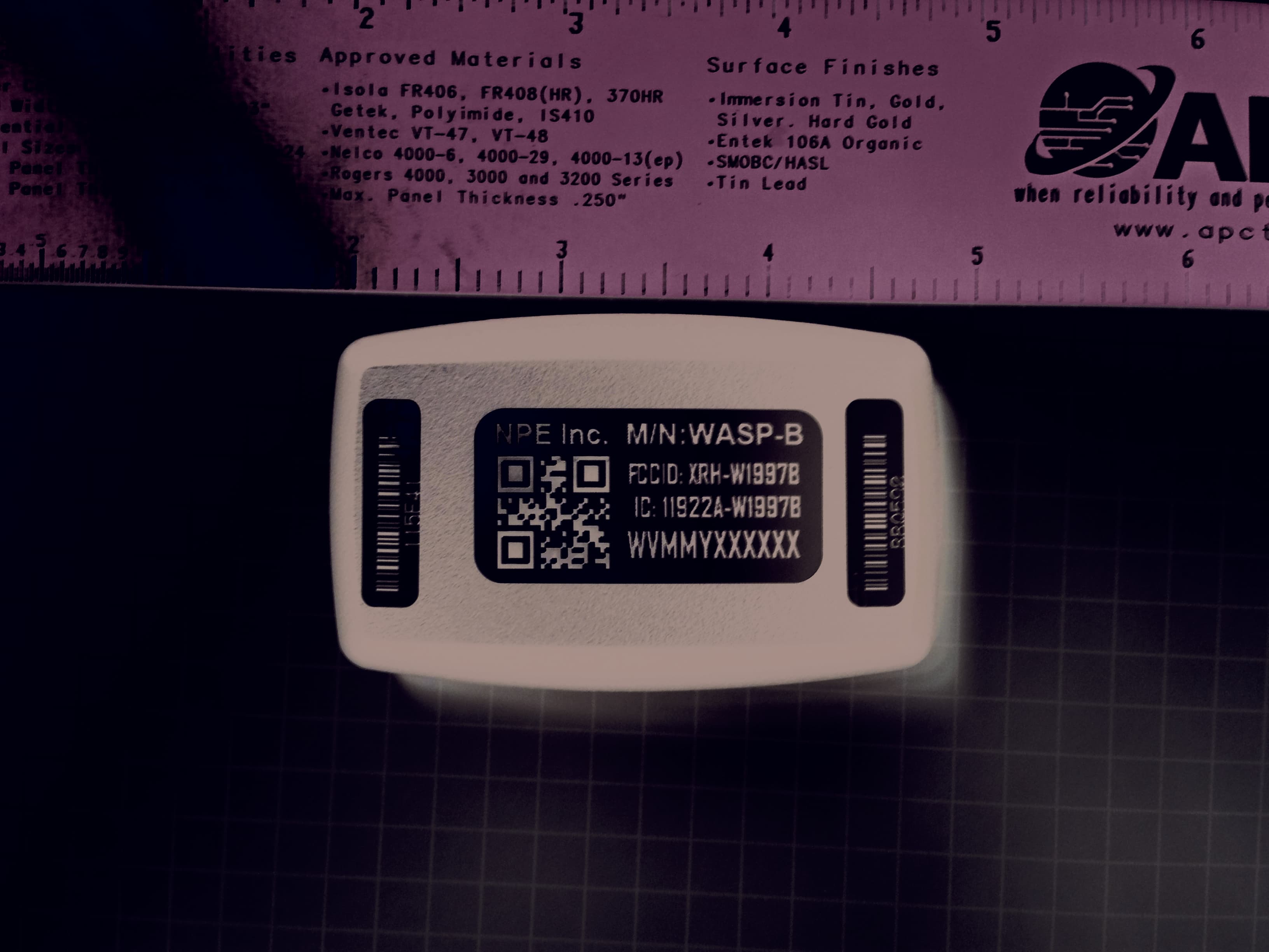
XRH-W1997B
May 20, 2014WiFi to ANT+ bridge device. Battery powered or DC wall supply powered.
Equipment Class
DTS - Digital Transmission System