Y2NRC1290Low power wireless communication module
Radiocrafts AS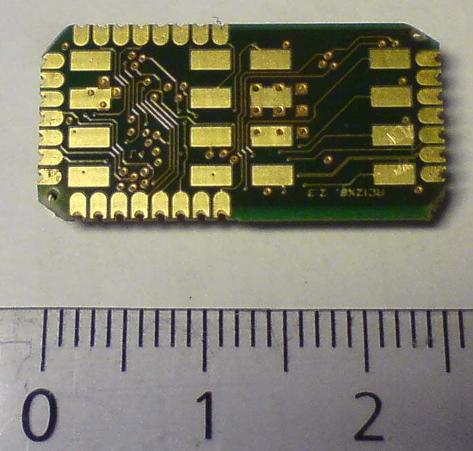
Click to zoom
Application Details
- Equipment Class
- DXX - Part 15 Low Power Communication Device Transmitter
- Date of Grant
- Jun 28, 2011
- Application Purpose
- Original Equipment
- Date of Application
- Jun 28, 2011
- Equipment Note
- Low power wireless communication module
- Frequency Range
- 902.50000000 - 927.50000000
- Company
- Radiocrafts AS
- Country
- Norway
Documents & Files
Document Text
Text extracted from the exhibit documents filed with the FCC. Open a document above to read the original.
Users Manual
Radiocrafts Embedded Wireless Solutions RC1240/1280/1290 ©2011 Radiocrafts AS RC1240/RC1280/RC1290 Data Sheet (rev. 1.62) Page 1 of 26 Narrow Band Multi-Channel RF Transceiver Module Product Description The RC1240, RC1280 and RC1290 RF Transceiver Modules are compact surface-mounted high performance modules for 25 kHz narrow band FSK operation with embedded protocol. The modules are completely shielded and pre-certified for operation under the European and US radio regulations for license-free use. When used with quarter-wave antennas a line-of- sight range of 2-4 km can be achieved at 433 MHz. Applications • OEM equipment • Radio modems • Alarm and security systems • Point-of-sales terminals • Bar code scanners • Telemetry stations • Fleet management Features • Smallest in the world (12.7 x 25.4 x 3.5 mm) • 25 kHz narrow band multi-channel operation • Very low current consumption, 3nA OFF mode • Embedded RC232™ protocol • Addressing and Error check • 128 byte data buffer • Simple UART interface for easy RS232/422/485 wire replacement • Compact shielded module for SMD mounting • No external components • No configuration required for single-channel use • Easy to use data interface, 3/5 V tolerant I/O • Wide supply voltage range, 2.8 – 5.5 V • Conforms with EU R&TTE directive (EN 300 220, EN 301 489, EN 60950) for 25kHz • Conforms with FCC CFR 47 part 15 Quick Reference Data Parameter RC1240 RC1280 RC1290 Unit Frequency band 433.05-434.79 868 – 870 902 – 928 MHz Number of channels 69 80 51 Channel bandwidth 25 25 25-100 kHz Data rate 4.8 4.8 1.2-19.2 kbit/s Max output power (typ) 8 7 4* dBm Sensitivity -115 -110 -110 dBm Supply voltage 2.8 – 5.5 Volt Current consumption, RX 20.2 20.7 20.7 mA Current consumption, TX 26 28 22.9** mA Current consumption, SLEEP 0.9 mA Current consumption, OFF 0.003 uA * Programmable. Maximum allowed radiated power under FCC CFR 47, part 15 is -1 dBm ERP. This give ** Apply for -1 dBm. Radiocrafts Embedded Wireless Solutions RC1240/1280/1290 ©2011 Radiocrafts AS RC1240/RC1280/RC1290 Data Sheet (rev. 1.62) Page 2 of 26 Typical Application Circuit GND CTS/RXTX/RXEN RTS/TXEN CONFIG TXD/SCL RXD/SDA GND GND VCC ON/OFF VDD GND RF GND 2.8 - 5.5 V Antenna { To host MCU or RS232/422/485 driver NC Quick Product Introduction How do I transmit data? Send your data to the RXD pin on the module. Use the UART format with settings (19200, 8, 1, N, no flow control), use 2 stop-bits if CTS is enabled. Up to 128 bytes are buffered in the module. The module will transmit the data when • the max packet length is reached • the unique end character is sent • the modem timeout limit is reached The packet length, end character and timeout limit are configurable in-circuit. How do I receive data? Any received data packet with correct address and check sum will be sent on the TXD pin using the same UART format as for transmit. What about the antenna? In most cases a simple quarter wavelength wire or a PCB track will do. Connect a piece of wire to the RF pin with length corresponding to the quarter of a wavelength. For space limited products, contact Radiocrafts and we will recommend the best antenna solution for your application. How do I change the RF channel or any other parameter? To change configurable parameters, assert the CONFIG pin, and send the command string using the same serial interface as for transmitting data. Parameters can be changed permanently and stored in non-volatile memory in the module. Radiocrafts Embedded Wireless Solutions RC1240/1280/1290 ©2011 Radiocrafts AS RC1240/RC1280/RC1290 Data Sheet (rev. 1.62) Page 3 of 26 Pin Assignment GND CTS/RXEN/RXTX RTS/TXEN CONFIG TXD/SCL RXD/SDA GND GND VCC ON/OFF VDD GND RF GND 1 2 3 4 5 6 7 14 13 12 11 10 9 8 15 16 17 18 19 20 21 22 30 29 28 27 26 25 24 23 Pin Description Pin no Pin name Description Equivalent circuit 1 GND System ground GND 2 CTS/RXTX/RXEN UART Clear to Send, UART RXTX, Receive Mode Enable, or SLEEP mode activation. Connect to VDD if not used. Internal 100 kΩ series resistor. 3 RTS/TXEN UART Request to Send, Transmit Mode Enable, or SLEEP mode activation. Connect to VDD if not used. Internal 100 kΩ series resistor. 4 CONFIG Configuration Enable. Active low. Should normally be set high. Connect to VDD if not used. Internal 100 kΩ series resistor. 5 TXD/SCL UART TX Data, or serial data clock. Internal 100 kΩ series resistor. 6 RXD/SDA UART RX Data, or serial data I/O. Internal 100 kΩ series resistor. 100k Input:VDD (2.7V) 100k VDD (2.7V) Output: 7 GND System ground 8 GND System ground GND 9 RF RF I/O connection to antenna 220p 10k RF Radiocrafts Embedded Wireless Solutions RC1240/1280/1290 ©2011 Radiocrafts AS RC1240/RC1280/RC1290 Data Sheet (rev. 1.62) Page 4 of 26 10 GND System ground GND 11 VDD Supply voltage output, regulated. Should normally be left open 2.7 V VREG 2.7 V VREG 2u2 VDD 12 ON/OFF Module on/off (shutdown). ON when high, OFF when low. For threshold see Electrical Specifications. Or connect to VCC. See important note under Power Management page 7. ON/OFF 13 VCC Supply voltage input. Internally regulated. Maximum rise-time requirement apply, see Electrical Specification. 2.7 V VREG 2.7 V VREG 2u2 VCC 14 GND System ground GND 15-21 RESERVED Test pins or pins reserved for future use. Do not connect! 22 RESET Main reset (active low). Should normally be left open. Internal 100 kΩ pull-up resistor, no series resistor. VDD (2.7V) RESET 100k 23 PA_EN External PA enable output, active high 24 LNA_EN External LNA enable output, active high VDD (2.7V) 25-30 RESERVED Test pins or pins reserved for future use. Do not connect! Note 1: In UART mode the TXD and RXD are used for serial data, and CTS/RXTX and RTS for flow control (optional). If flow control is not used, and RXEN and TXEN are both asserted (active low) the module is set in SLEEP mode. RXEN and TXEN should be connected to VDD if not used if not used for SLEEP mode activation. A pull-up resistor is not necessary due to an internal series resistor.…
Text truncated - open the document above for the full version.
Cover Letter(s)
Radiocrafts Embedded Wireless Solutions Radiocrafts AS, Oslo Adresse/Address: Sandakerveien 64 NO-0484 OSLO NORWAY Attn: Reviewing Engineer Federal Communications Commission Tel: (+47) 4000 5195 Fax: (+47) 22 71 29 15 Web: www.radiocrafts.com E-mail: [email protected] Foretaksnr./Enterprise No.: NO 985 876 096 MVA Deres ref. / Your ref. Vår ref. / Our ref. Tlf. direkte / Direct Line Oslo, To Whom It May Concern: Pursuant of Section 0.457 and 0.459 of the FCC Commission's Rules we hereby request confidentiality for documents given below. Letter cover FCC ID: Y2NRC1290 We request that the - Schematic diagrams - Part list /Bill of Material (BOM) - Block diagrams - Technical descriptions submitted with this application, are withheld from public review. The documents are company proprietary information that should never get into the possession of our competition. Please contact me if there is any information you may need. Sincerely, Radiocrafts Ørjan Nottveit
Cover Letter(s)
Radiocrafts Embedded Wireless Solutions Radiocrafts AS, Oslo Adresse/Address: Sandakerveien 64 NO-0484 OSLO NORWAY Attn: Reviewing Engineer Federal Communications Commission Tel: (+47) 4000 5195 Fax: (+47) 22 71 29 15 Web: www.radiocrafts.com E-mail: [email protected] Foretaksnr./Enterprise No.: NO 985 876 096 MVA Deres ref. / Your ref. Vår ref. / Our ref. Tlf. direkte / Direct Line Oslo, To Whom It May Concern: This letter serves as an official request for a Modular Approval. A full modular approval is being requested for the FCC ID: Y2NRC1290 Model number: RC1290 With reference to FCC §15.212, the FCC ID: Y2NRC1290 is characterized by: i) The module has its own RF shielding that prevents coupling between the RF circuitry of the module and any wires or circuits in the device which the module is to be installed ii) The module have buffered data inputs. iii) The RF output power level control, the frequency synthesizers and modulator are all powered from an internal low-drop power regulator to ensure FCC-compliance regardless of the design of the power supplying circuitry in the device into which the module is installed. iv) The module has an antenna connection as a non-standard connection point(solering point) v) The module has been tested in a stand-alone configuration, only using an open PCB carrier as test jig. - PCB routes the power directly to the pins of the module. No ferrite or regulator were used in between. DC lines are soldered to two pins close to module and the signals are then routed to the pads on module with PCB traces. DC lines are more than 10 cm. - The PCB have no other function that connection of signals to module. As such it operates as a test jig. No filter function or ferrite on any signals. vi) The module is labeled with it own FCC ID number. This marking will be repeated on the outside of the device where the module is to be installed. 2 vii) The module is supported with a Datasheet/User Manual that gives instructions on how to install and operate the module in order to comply with the regulations. _________________________ _2011-06-27___ Ørjan Nottveit Date
External Photos
TOP BOTTOM
ID Label/Location Info
Label location Model: RC1290 FCC ID: Y2NRC1290 IC: 9402A-RC1290 201050rev 1.04
Internal Photos
TOP BOTTOM
Test Report
Nemko AS, Gaustadalléen 30, P.O.Box 73 Blindern, NO-0314 Oslo Norway T +47 22 96 03 30 F +47 22 96 05 50 Enterprise number NO974404532 Visiting address: Nemko Kjeller, Instituttveien 6, P.O.Box 96, NO-2027 Kjeller Norway T +47 64 84 57 00 F +47 64 84 57 05 Test report no. : 175366-3 Item tested : RC1290 Type of equipment : Low power Transceiver 902 - 928MHz Evaluation Module FCC ID : Y2NRC1290 Client : Radiocrafts AS FCC Part 15.249 Low Power Transceiver 902-928 MHz Band RSS-210, Issue 8 and RSS-GEN, Issue 3 Low-Power Licence-exempt Radiocommunications devices 902 – 928 MHz Band 31 May 2011 Authorized by : .............................................. Frode Sveinsen Technical Verificator TEST REPORT FCC part 15.249 Project no.: 175366-3 FCC ID: Y2NRC1290 Nemko AS, NO-2027 Kjeller Page 2 (66) CONTENTS 1 GENERAL INFORMATION ...................................................................................................... 3 1.1 Testhouse Info .......................................................................................................................... 3 1.2 Client Information ...................................................................................................................... 3 1.3 Manufacturer ............................................................................................................................. 3 2 Test Information ...................................................................................................................... 4 2.1 Test Item ................................................................................................................................... 4 2.2 Test Environment ...................................................................................................................... 5 2.2.1 Normal test condition ................................................................................................... 5 2.3 Test Period................................................................................................................................ 5 3 TEST REPORT SUMMARY ..................................................................................................... 6 3.1 General ..................................................................................................................................... 6 3.2 Test Summary ........................................................................................................................... 7 3.3 Description of modification for Modification Filing ..................................................................... 7 3.4 Comments ................................................................................................................................ 7 3.5 Family List Rationale ................................................................................................................ 7 4 TEST RESULTS ....................................................................................................................... 8 4.1 Power-line Conducted Emissions ............................................................................................. 8 4.2 Transmitter Frequency Stability .............................................................................................. 10 4.3 20 dB Bandwidth ..................................................................................................................... 11 4.4 Peak Power Output ................................................................................................................. 21 4.5 Band Edge Emissions ............................................................................................................. 37 4.6 Spurious Emissions (Radiated) .............................................................................................. 40 4.7 Receiver Spurious Emissions (Conducted) ............................................................................ 60 5 LIST OF TEST EQUIPMENT .................................................................................................. 64 6 BLOCK DIAGRAM ................................................................................................................. 65 6.1 System set up for radiated measurements ............................................................................. 65 6.2 Power line Conducted Emission ............................................................................................. 65 6.3 Test Site Radiated Emission ................................................................................................... 66 TEST REPORT FCC part 15.249 Project no.: 175366-3 FCC ID: Y2NRC1290 Nemko AS, NO-2027 Kjeller Page 3 (66) 1 GENERAL INFORMATION 1.1 Testhouse Info Name : Nemko AS Address : Nemko Kjeller Instituttveien 6, Box 96 NO-2027 Kjeller, NORWAY Telephone : +47 64 84 57 00 Fax : +47 64 84 57 05 Email: [email protected] FCC test firm : 994405 IC OATS : 2040D-1 Total Number of Pages: 66 1.2 Client Information Name : Radiocrafts AS Address : Sandakerveien 64, 0484 Oslo, Norway Telephone : +47 40 00 51 95 Fax : -- Contact: Name : Ørjan Nottveit Telephone : +47 40 00 51 95 E-mail : [email protected] 1.3 Manufacturer Same as client TEST REPORT FCC part 15.249 Project no.: 175366-3 FCC ID: Y2NRC1290 Nemko AS, NO-2027 Kjeller Page 4 (66) 2 Test Information 2.1 Test Item Name : Radiocrafts Model/version : RC1290 Serial number : - Hardware identity and/or version: - Software identity and/or version : - Frequency Range : 902.5 – 927.5 MHz Tunable Bands : 1 Number of Channels : 51 1 Operating Modes : TX & RX Type of Modulation : FSK Emissions Designator : F1D User Frequency Adjustment : None, Software controlled Output Power (Conducted) : 0.3 mW Type of Power Supply : 2.8 - 5.5 V DC Antenna Connector : Reversed SMA Antenna Diversity Supported : None 1) Only one channel in use at a time. Theory of Operation The RC1290 RF-transceiver module for the 902-928 MH…
Text truncated - open the document above for the full version.
Test Setup Photos
FCC ID: Y2NRC1290 Project no.: 175366 Page 1 of 2 PHOTOS OF TEST SET-UP Radiated Emissions Test FCC ID: Y2NRC1290 Project no.: 175366 Page 2 of 2 Power line Conducted Emissions Test
Contact Information
Applicant
Orjan Nottveit
Technical Contact
Non-Technical Contact
Radiocrafts AS�rjan Nottveit
[email protected]+47 917 69 453
Test Firm
Nemko ASFrode Sveinsen
Technical Specifications
| # | Rule Parts | Frequency Range | Power Output |
|---|---|---|---|
| 1 | 15C | 902.5 MHz - 927.5 MHz | - |
Other Applications from Radiocrafts AS
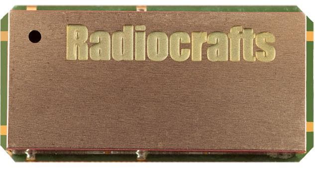
Y2NRC189XHP-IPM
Mar 27, 2023A Wireless Communication Mesh Network in a Module
Equipment Class
DSS - Part 15 Spread Spectrum Transmitter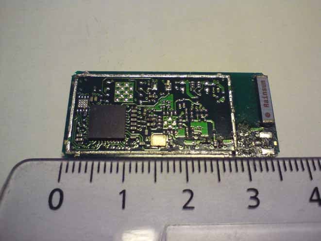
Y2NRC24XX
Apr 13, 2011Low power wireless communication module
Equipment Class
DTS - Digital Transmission System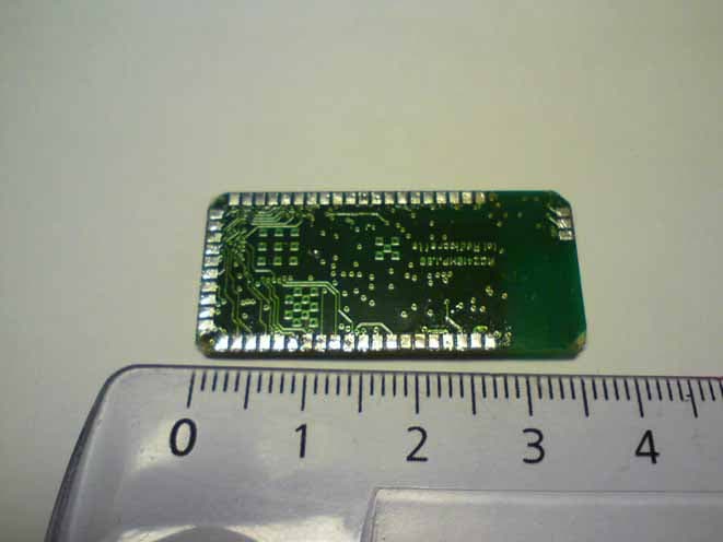
Y2NRC24XXHP
Apr 13, 2011Low power wireless communication module
Equipment Class
DTS - Digital Transmission System