Y4N70209TMobiCam DXR Touch Wireless Monitoring System
Mobi Technologies, Inc.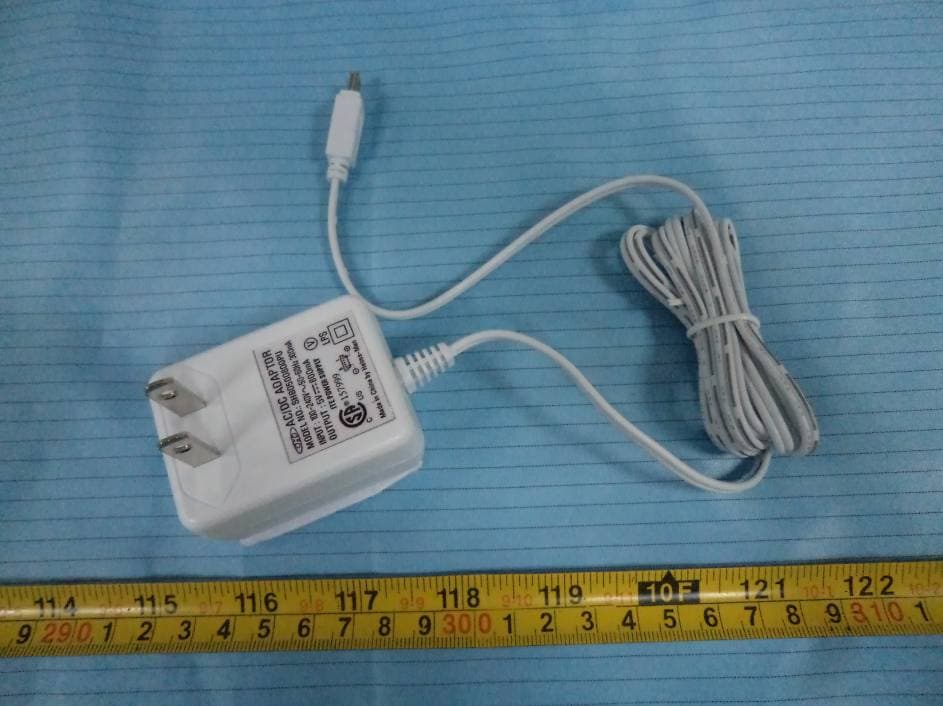
Click to zoom
Application Details
- Equipment Class
- DSS - Part 15 Spread Spectrum Transmitter
- Date of Grant
- Feb 10, 2013
- Application Purpose
- Original Equipment
- Date of Application
- Feb 10, 2013
- Equipment Note
- MobiCam DXR Touch Wireless Monitoring System
- Frequency Range
- 2410.87500000 - 2471.62500000
- Company
- Mobi Technologies, Inc.
- Country
- United States
Documents & Files
Document Text
Text extracted from the exhibit documents filed with the FCC. Open a document above to read the original.
Users Manual
IMPORTANT: Keep instructions for future reference. 70208 Complete Operating Instructions Complete Operating Instructions Complete Operating Instructions 1 INTRODUCTION Congratulations on the purchase of this MobiCam® DXR Touch Monitoring System, which incorporates the latest advanced technology. To fully maximi- ze and benefit from this product’s avanced features we hightly recommend you review these instructions. This 2.4 GHz Digital monitor enables you to transmit picture and sound signals cordlessly, which is ideal for many situa- tions suchs as monitoring a baby, young children or the elderly or used as office or warehouse monitoring system. RADIO INTERFERENCE PARAMETERS FCC Statement 15.19: This device complies with part 15 of the FCC Rules. Operation is subject to the following two conditions: (1) This device may not cause harmful inter- ference and (2) This device must accept any interference received, including interference that may cause undesired operation. 15.21: Changes or modifications not expressly approved by the party respon- sible for compliance could void the user’s authority to operate the equipment. FCC Radiation Exposure Statement This equipment has been tested and complies with Federal Communications Commission radiation exposure limits as set forth for uncontrolled environ- ments. This equipment should be installed and operated with minimum distance 20cm between the radiator and your body. This Camera must not be co-located or operating in conjunction with any other antenna or Cam- era. This equipment complies with FCC RF radiation exposure limits set forth for an uncontrolled environment. This device and its antenna must not be co-located or operating in conjunction with any other antenna or Camera. This device has been tested for compliance with FCC RF Exposure (SAR) limits in the typical laptop computer configuration and this device can be used in desktop or laptop computers via side mounted USB slots. This device and its antenna must not be co-located or operated in conjunction with any other antenna or Camera. IC Statement Operation of this device is subject to the following two conditions: 1. This device may not cause interference, and 2. This device must accept any inter- ference, including interference that may cause undesired operation of the device. TABLE OF CONTENTS Introduction 1 Radio Interferece Parameters 1 Package Contents 2 Monitor/Receiver 2 Camera/Transmitter 3 To Start Charging/Powering On 4 Locking the Screen 4 Set to Another Language 4 Pairing Camera and Monitor 5 Main Menu 6 Touch Navigation Volume/Display 7 Lullabys 7 Night Light 7 Record 8 Play 9 Quad and Channel View 10 VOX (Voice Activation) 10 Settings Monitor Settings 11-14 Camera Settings 15 Per Camera and Convenience Icons 16 Webcam Use • Data/File Transfers 17 Audio/Video Out 18 Troubleshooting 18 Factory Default Settings 19 Battery Replacement 20 Product Safety 20 Proper Disposal 21 Limited Warranty 21 About Mobi® / Contact Mobi® 22 IMPORTANT: Use ONLY a fingertip or other NON-SHARP object to select touch screen options. Using sharp objects can damage the screen and void the warranty. 23 CAMERA MONITOR PACKAGE CONTENTS • 1 Monitor/Receiver • 1 Camera/Transmitter • 2 AC/DC Adaptors 5V 800mAh • 1 Li-Ion Rechargeable Battery (for monitor only) • 1 Attachable Strap Mount • 1 Door/Drawer Attachable Hook • 1 Wall Anchor Mount with Screw • 1 USB to Mini USB Data Cord • 1 AV-Out Cable • 1 User Manual PAIR Button Strap Mount (underneath) Power ON LED Indicator Camera Lens Night Light Night Vision IR LEDs DC Power Input 2-Way Talk / Lullaby Speaker Microphone ON / OFF Button Battery Compartment Retractable Antenna Ridge-Grip Surface Stand Positioning/Mounting Options A. Horizontal to Slightly Angled Surfaces - Built-in Ridge-Grip Feet... B. Wall Mount Screw with Drywall Anchor (included)... C. Door or Drawer Hook Mount / Stand (included)... D. Horizontal Rails / Drawer Handles - Attachable Strap Mount (included) Camera / Transmitter Unit features: • PAIR Button • LED for Power ON / Pairing (flashes) • Microphone & Speaker • DC Input (AC/DC adaptor included) • Night Vision • Temperature Sensor and Alarm • VOX (Hi/Mid/Lo/Off) with receiver control • Adjustable Volume from receiver • Adjustable TX Power (High-Low) from receiver • 4 Lullaby choices • Night Light • Rechargeable Battery 3.7V 1500 mAh (not included - sold separately) • 2.4GHz Digital FHSS, 100% secure with full privacy and interference free Monitor / Receiver Unit features: • 3.5” QVGA resolution TFT touch panel screen • VGA resolution (640*480) up to 25 frames per second • up to 250-300m range • 2-way communication • MENU/ESCAPE button • PAIR Button • TALK Button • Lock Screen Button for disabling touch screen • SD Card Slot up to 32 Gb (not included) • Mini USB Output port (for connection to a PC and charging) Power ON LED Indicator Retractable Antenna 2-Way Talk Speaker ON/OFF Button Lock Screen Button Battery Compartment PAIR Button Combo Screen Cover / Fold-back Stand Escape/Menu Button 2-Way Talk Button AV Output DC Power Input / Mini USB Output 2-Way Talk Microphone SD Card Slot (card not included) • A/V Output port • DC Input (AC/DC adaptor included) • Two-Color LED: solid green for power on; flashing red for charging • Quad-View split screen (up to 4 camera capability) • Main Menu color icon display • Rechargeable Li-ion Battery 3.7V 1200 mAh (included for monitor only) A.B. C.D. A.B. C.D. WARNING: To prevent strangulation never place a power cord within reach of a child. TO START A. Plug one of the AC/DC adapters (they are interchangeable) into the monitor and allow it to charge the Monitor Battery for at least 5-1/2 hours. B. Plug the other AC/DC adapter into the camera. Turn the Camera On by holding the ON/OFF Button down for several seconds. The green “Power On” Indicator lights when powered up. C. Turn the Monitor On by holding its ON/OFF Button down for several seconds. Its “Power On” Indicator will light up (green on…
Text truncated - open the document above for the full version.
Block Diagram
SN93500 SN93500SN93500 SN93500 CONTROL UNIT CONTROL UNITCONTROL UNIT CONTROL UNIT (For Baby Unit ) (For Baby Unit )(For Baby Unit ) (For Baby Unit ) Power adaptor jack Power adaptor jackPower adaptor jack Power adaptor jack Status indicator LED Status indicator LEDStatus indicator LED Status indicator LED COMS sensor COMS sensorCOMS sensor COMS sensor Microphone AMP. Microphone AMP.Microphone AMP. Microphone AMP. ID code setting button ID code setting buttonID code setting button ID code setting button RF module RF moduleRF module RF module Speaker AMP. Speaker AMP.Speaker AMP. Speaker AMP. ANT Crystal CrystalCrystal Crystal Y1 Y1Y1 Y1 12MHz 12MHz12MHz 12MHz 2.4GHz
Cover Letter(s)
MOBI TECHNOLOGIES INC. 5913 BLACKWELDER STREET CULVER CITY, CA 90232, USA Tel: 877-662-4462 Fax: 424-672 6628 FCC Authorization 2013-2-5 FEDERAL COMMUNICATIONS COMMISSIONS Authorization and Evaluation Division 7435 Oakland Mills Road Columbia, MD 21046 Subject: Agent Authorization To whom it may concern: We MOBI Technologies, Inc. , the undersigned, Hereby authorizes Bay Area Compliance Laboratories Corporation to act on its behalf in all matters relating to application for Equipment authorization, including the signing of all documents relating to these matters. All acts carried out by Bay Area Compliance Laboratories Corp. On our Behalf shall have the same effect as our own action. We, the undersigned, hereby certify that we are not subject to a denial of federal benefits, that includes FCC benefits, pursuant to Section 5301 of the Anti-Drug Abuse Act of 1988, 21 U.S.C. 853(a). This authorization is valid until further written notice from the applicant. Sincerely Yours, David Naghi President
External Photos
EXHIBIT B - EUT EXTERNAL PHOTOGRAPHS EUT – Front View EUT – Rear View EUT – Top View EUT – Bottom View EUT – Left Side View EUT – Right Side View EUT – Unfold View EUT – Adapter View EUT – Adapter Label View
ID Label/Location Info
EXHIBIT A - FCC ID LABELING AND LOCATION FCC ID Label FCC ID Label Location The label shown shall be permanently affixed at a conspicuous location on the device and be readily visible to the user at the time purchase (Labeling requirements per 2.925) Label here
Internal Photos
EXHIBIT C - EUT INTERNAL PHOTOGRAPHS EUT – Battery off View EUT – Cover off View EUT – Main Board Top Board View EUT – Main Board Top Shielding off View Antenna EUT – Main Board Bottom View EUT – Power Board Top View EUT – Power Board Bottom View EUT – Battery View
Operational Description
Circuit Description 1.The Circuit structure The receiver utilizes single conversion.The IF is 4.5MHz,The local oscillators signal both for TX and RX are supplied from the crystal oscillator circuit.. 2.Receiver System. 1).RF AMP. The RF signal coming from the antenna passes through harmonic filter (LPF) consisting of U4 to filter out the unwanted signals, the antenna switching circuit (U5),and is amplified by RF low-noise-Amplifier Q3,and goes to the mixer. 2)Mixer The signal from the front end is mixed with the local oscillator signal generated in the crystal oscillator by U2 to the produce IF of frequency of 4.5MHz. 3.Local oscilltor Transmitter:RF modules 18MHz(C31, C32, Y1) and SN93500 IC of the 12MHz(C69, C671,X1) component. 4.Launchers system 1).Transmit audio TX wheat drive through the first to voice signals into electricalsignals though IC2(LM4890) to enlarge an operational amplifierand then after the second class , Composed of hight-frequency extraction filter bandwidth of 20-30kHz of the electrical signal and then to ADC(in SN93500) converted to PCM DATA,though the SPIport module output to RF7121 sent. 2)Video transmission Transmitter though the U8(OV7670) to obtain images,compressed by SN93500 IC output though the SPI port to RF7121 module . 3)Modulation and RF amplifier Basically ,audio and video packets in the A7121 though the RFmodulator ,PA after U3(AP1110) after amplification(U4) BF2520 launch out. 4)ANT switch and LPF Mainly by the antenna switch U5(HWS314) processing ,the signal input and output filter by U4(BF2520) to deal with. 5. The cmposition of power The input 6V power or 3.7V battery power ,by a 3.3V voltage regulator U3 to RF module,U5 from 3.3v voltage regulator power supply to SN93500 and amplifier IC2.
Operational Description
Channel No. Frequency (MHz) 0 2410.875 1 2414.25 2 2417.625 3 2421 4 2424.375 5 2427.75 6 2431.125 7 2434.5 8 2437.875 9 2441.25 10 2444.625 11 2448 12 2451.375 13 2454.75 14 2458.125 15 2461.5 16 2464.875 17 2468.25 18 2471.625 working channel An explanation on Frequency Hopping system 1. Scope of frequency used in this product is limited between 2410.875 MHz and 2471.625 MHz, which is dividedinto 19 channels (channel 0 to channel 18) with an interval of 3.375 MHz every two channels, and each channel ‘sworking time is 4.04 ms, in which TX keeps transmitting for 3.68 ms, and at non-transmitting state for 0.36 ms.2. The initial serial numbers of difference pairs aren't identical because it is a fixed serial number of frequencyhopping for every pair of units, which is generated when establish code link, also, acquired manner of frequencyhopping of every pair is at random. It hop 248 times per second.3. Below is the corresponding table of channels No. and channels’ frequencies.
Schematics
Title Number Revision Size A4 Date: 19-Jun-2012 Sheet of Drawn By: C34104P DGND GND-TV RF-TXD RF-RX-SEL RF-RXD RF-SPI-CS RF-SPI-CLK RF-SPI-IN VDD33 DGND VDD18 DGND C35 104P C36104P RF-SPI-OUT RF-ANT1 RF-ANT2 RF-PA RF-CE RF-TX-SEL GPIO0(NIG) GPIO3(4890) GND-ADC VDD33-ADC AIN2 C37104P TXRX DGND VDD33 C40 104P DDR-VREFDGNDVDD25VDD18DGNDVDD25 C38 104P DGND C39 104P C42 104P C41104P VDD25DGNDDGNDVDD25DGNDVDD18VDD25DGNDRTC-XINRTC-XOUTVDD-RTC C43104P C27 104P C26 104P DGND KEY VDD18-PLL4 VDD33 DGND DGND VDD18-PLL3 VDD33 VDD18-PLL1 DGND VDDL18 VDD33 OUTR VDD33-DAC GND-DAC OUTL DGND RST XOUT XIN VDD33 DGND VDD18 C16 104P C17104P DGND C18 104P R3056K DGND VDD33 C19 104P GND-DAC C20 104P C4105P DGND VDD25DGNDVDD18VDD25DGNDVDD25DGNDDGNDVDD25VDD18DGNDVDD25SF-CSSF-SOSF-SISF-SCKS-HSYNCS-VSYNCS-PCK VDD33 C14104P C12 104P C15104P C13104P C31 104P C30 104P C32104PC33104P DGNDDGND 1234 5678 U7MX25L8006E R40 1K SF-CSSF-SI VDD33 C44104P VDD33 SF-SCK SF-SO X112MHZ C6922PC7022P DGND XINXOUT GND 1234 J2CON4 R381K TXRX RTC-XINRTC-XOUT DGND C71 20P C7220P X2 32.768Khz VDAC-VREF 1 VDAC-REG 2 VDD-TV 3 GND-TV 4 RF-TVD/GPIO 5 RF-RX-SEL/GPIO 6 RF-RXD 7 RF-SPI-CS/GPIO 8 RF-SPI-CLK 9 RF-SPI-IN 10 VDD33 11 GND 12 VDD18 13 RF-SPI-OUT/GPIO 14 RF-ANT1/GPIO 15 RF-ANT2/GPIO 16 RF-PA/GPIO 17 RF-CE/GPIO 18 RF-TX-SEL/GPIO 19 GPIO0/PWM-A0 20 GPIO1/PWM-A1 21 GPIO2/PWM-A2 22 GPIO3/PWM-A3 23 GND-ADC 24 PGA-P-L 25 PGA-N-L 26 PGA-P-R 27 PGA-N-R 28 VDD-ADC 29 AIN1-L 30 AIN1 31 AIN2 32 AIN3 33 TX/DMIC-CLK/GPIO 34 RX/DIMC-DI/GPIO 35 SD-CLK/GPIO 36 SD-CMD/GPIO 37 GND 38 VDD33 39 USB-DET 40 SD-D0/GPIO 41 SD-D1/GPIO 42 SD-D2/GPIO 43 SD-D3/GPIO 44 TEST 45 GND 46 DDR-VREF 47 GND-DDR 48 VDD25 49 VDD18 50 GND-DDR 51 VDD25 52 GND-DDR 53 VDD25 54 GND-DDR 55 VDD25 56 GND-DDR 57 VDD18 58 VDD25 59 GND-RTC 60 RTC-XIN 61 RTC-XOUT 62 VDD-RTC 63 RTC-CTL 64 KEY 65 VDD18-PLL4 66 VDD-USB 67 GND-USB 68 DM 69 DP 70 GND-PLL3 71 VDD18-PLL3 72 VDD-PLL 73 VDD18-PLL1 74 GND-LVD 75 VDDL18 76 VDD-LVD 77 OUTR 78 VDD-DAC 79 GND-DAC 80 OUTL 81 GND 82 RST 83 GPIO4/PWM-B0/I2S-MCLK 84 GPIO5/PWM-B1/I2S-LRCK 85 GPIO6/PWM-B2/I2S-BCLK 86 GPIO7/PWM-B3/I2S-DAT-IN 87 GPIO8/I2S-DAT-OUT 88 GPIO9 89 XOUT 90 XIN 91 VDD33 92 GND 93 VDD18 94 I2C-SCL/LCD-IO11/GPIO 95 I2C-SDA/LCD-IO12/GPIO 96 VDD25 97 GND-DDR 98 VDD18 99 VDD25 100 GND-DDR 101 VDD25 102 GND-DDR 103 GND-DDR 104 VDD25 105 VDD18 106 GND-DDR 107 VDD25 108 SF-CS 109 SF-SO 110 SF-SI 111 SF-SCK 112 S-HSYNC/LCD-IO0 113 S-VSYNC/LCD-IO1 114 S-PCK/LCD-IO2 115 SEN-CLK/LCD-IO16 116 GND 117 VDD33 118 S-IMG0/LCD-IO10 119 S-IMG1/LCD-IO9 120 S-IMG2/LCD-IO8 121 S-IMG3/LCD-IO7 122 S-IMG4/LCD-IO6 123 S-IMG5/LCD-IO5 124 S-IMG6/LCD-IO4 125 S-IMG7/LCD-IO3 126 I-OUT 127 I-OUTB 128 U6 SN93500 C24104P C25104P DGND C23 104P C22 104P C21104P DGND DGND R360R VDD33 R320R VDDL18 VDD18-PLL4VDD18-PLL3 VDD18 R310R R33 0R R35 0R R34 0R VDD18-PLL1 VCC18 AIN1 AIN1-L I2C-SCL I2C-SDA S-IMG0S-IMG1S-IMG2S-IMG3S-IMG4S-IMG5S-IMG6S-IMG7SEN-CLK MIC-N-L MIC-P-L R5010M GPIO6(LED) AIN3 RTC-CTL VDD33 GPIO7(SRESET) GPIO4(PWN) R52200K+-1%R51300K+-1% R53390K C45104P R391K LED12POWER GPIO6(LED) VDD VDD-RTC AIN1-L AIN1 BAT R4218K+-1% C28104P AIN3 TR1 10K VDD33 K1 CODE R17100K AIN2 VDD33 R100RR190R C91475P VDD33 VDD33-ADC GND-ADC R620RR630R C92106P VDD33 VDD33-DAC GND-DAC DP DM GPIO2 P3 P1 P2 P4 GPIO8 GPIO9 GPIO5 VSS 1 PWMP 2 VSD 3 PORTA0 4 PORTA1 5 PORTA2 6 PORTA3 7 PORTA4 8 PORTA5 9 PORTA6 10 PORTA7 11 PORTB1 12 PORTB0 13 HALT 14 VPPX 15 PWMN 16 U10TRD16P102B SOSISCKCS C88104P VDD33 AGND R841K R7610K C87104P PWMOUT AGND C98 473P C90104P AGND R2 100R R65100R R64100R GPIO9GPIO8GPIO5 R770R 1234 5678 U11MX25L1606E R85 1K CSSO VDD33 C97104P VDD33 SCK SI AGND File: Title Number Revision Size A4 Date: 19-Jun-2012 Sheet of Drawn By: C11104P C5310UF R1230KR13300K R610K Q33904 R18680R R15100K R71M Q2SI2301 S1 POWER KEY VCC 12 3 D3BAT54C RTC-CTL VDD 2.4G RF C5410UF C61 104P VCC VDD25 IN 1 GND 2 EN 3 BP 4 OUT 5 U2CE75B25M C63 104P C56 10UF C5510UF C62 104P VCC IN 1 GND 2 EN 3 BP 4 OUT 5 U3CE75B33M C64 104P C57 10UF VDD33-RF C66102P C65102P EN 1 GND 2 LX 3 VIN 4 FB 5 U4CE2403ADJ L3 22UH C59 106P R2675K+-1% R2718K+-1% C58 106P R810K EN 1 GND 2 LX 3 VIN 4 FB 5 U5 CE2403ADJ L4 2.2UH C67 475P R29 36K+-1% R2818K+-1% C3 105P R910K VCC VCC VCC VCC VDD33 VCC18 1234 5678 IC2LM4890 C8105P C7105P GND-MIC C49104P C77103P R453K3 R483K3 GND-MIC R60 200K R473K3 R493K3 C75 100P C52104P GND-MIC MIC-P-L MIC1MIC R25100R C50104P C51104P C7847U GND-MIC VDD33 C29104P C68100U GND-MIC 1 2 3 D5 BAT54S Q4 3904 R11 10K R5847K GND-MIC C60106P R370R R610R C7910P C9105P GND-ADC C10105P MIC-N-L C46104P 1234 5678 IC3 LM4890 C6105P C5105P C73NC C47104P R555K1 R463K3 OUTL R56100K R591R C74 102P C48 104P LS18R/1W GPIO3(4890) VCC C76220UF PWMOUT R22 100R R23 100R R20 100R R21100R R24100R L20R RF-TX-SEL L1 0R RF-SPI-CS RF-SPI-CLK RF-SPI-IN RF-SPI-OUT RF-ANT2 RF-RXD RF-CE RF-PA RF-ANT1 R16 100K RF-RX-SEL VDD33-RF GND 1 TXSW 2 RXSW 3 SPI-CS 4 SPI-CLK 5 SPI-TXD 6 SPI-RXD 7 CO-TXEN 8 TRXD 9 RESETN 10 MS0 11 MS1 12 BB-CLK 13 VIN33 14 U1 A7121 2.4GRF R5751K VDD SW SWGPIO6(LED) VDDSWGPIO6(LED) LED1 LED LED10LED LED2LED R41100R Q68050 R54100R R7947KR14100K VDD GPIO0(NIG) R78100R R83470K C96106P C95225P R813K chrg 1 GND 2 BAT 3 VCC 4 prog 5 IC4LP4054 J1 DC6V BAT1 3V7 D21N5817 R82 3K3 Q7SI2301 D11N5817 D121I4148 R802K2 BAT POWER LED11CHRG GND GND 12345 CON2CON5 12345 CON1CON5 BAT BAT LED16 LED LED18LED LED17LED R86100R R87100R R88100R C10010P C10233P C9910P C10133P GND GND-MIC GND C10333P GND C662 103P C652 104P GND File: 1 2 34 ABCD 4 3 2 1 D CBA Title Number Revision Size A4 Date: 19-Jun-2012 Sheet of Drawn By: D0 B4 D1 A4 D2 B5 D3 A5 D4 F5 D5 E5 D6 F4 D7 E4 VSYNC D1 HREF D2 PCLK E1 SDA A2 XCLK E3 SCL A3 RESET F2 0 0/2 0/3 0/4 STROBE E2 PWDN B1 DOGND F3 DOVDD F1 DVDD C1 VREF2 B2 VREF1 C2 AGND B3 AVDD A1 U8OV7670 VDDA28 C93104P C94104P VDD28 R70NC GPIO4(PWN) R694K7R684K7R674K7 VDD28 S-IMG0S-IMG1S-IMG2S-IMG3S-IMG4S-IMG5S-IMG6S-IMG7 S-PCK S-VSYNCS-HSYNC SEN-CLK R5100R C110P GPIO7(SRESET) R3 68R R4 68R R4368R R44 68R R732KR74560K C8…
Text truncated - open the document above for the full version.
Test Report
Note: This test report is prepared for the customer shown above and for the equipment described herein. It may not be duplicated or used in part without prior written consent from Bay Area Compliance Laboratories Corp. This report must not be used by the customer to claim product certification, approval, or endorsement by NVLAP* or any agency of the Federal Government. * This report may contain data that are not covered by the NVLAP accreditation and shall be marked with an asterisk “★” FCC PART 15.247 TEST REPORT For Mobi Technologies, Inc 5913 BLACKWELDER STREET CULVER CITY, CA 90232, USA FCC ID: Y4N70209T Report Type: Original Report Product Type: Mobicam DXR Touch wireless Monitoring System(Baby unit) Test Engineer: Jimmy Xiao Report Number: RSZ130124005-00 Report Date: 2013-02-01 Reviewed By: Sula Huang RF Engineer Test Laboratory: Bay Area Compliance Laboratories Corp. (Shenzhen) 6/F, the 3rd Phase of WanLi Industrial Building ShiHua Road, FuTian Free Trade Zone Shenzhen, Guangdong, China Tel: +86-755-33320018 Fax: +86-755-33320008 www.baclcorp.com.cn Bay Area Compliance Laboratories Corp. (Shenzhen) Report No.: RSZ130124005-00 FCC Part15.247 Page 2 of 37 TABLE OF CONTENTS GENERAL INFORMATION.......................................................................................................................................4 PRODUCT DESCRIPTION FOR EQUIPMENT UNDER TEST (EUT) .....................................................................................4 OBJECTIVE...................................................................................................................................................................4 RELATED SUBMITTAL(S)/GRANT(S).............................................................................................................................4 TEST METHODOLOGY..................................................................................................................................................4 TEST FACILITY.............................................................................................................................................................4 SYSTEM TEST CONFIGURATION ..........................................................................................................................6 DESCRIPTION OF TEST CONFIGURATION......................................................................................................................6 EUT EXERCISE SOFTWARE..........................................................................................................................................6 EQUIPMENT MODIFICATIONS.......................................................................................................................................6 EXTERNAL I/O CABLE..................................................................................................................................................6 BLOCK DIAGRAM OF TEST SETUP................................................................................................................................6 SUMMARY OF TEST RESULTS...............................................................................................................................7 FCC §15.247 (i) & §1.1307 (b) (1) & §2.1091- MAXIMUM PERMISSIBLE EXPOSURE (MPE)..............................8 STANDARD APPLICABLE..............................................................................................................................................8 FCC §15.203 – ANTENNA REQUIREMENT ............................................................................................................9 APPLICABLE STANDARD..............................................................................................................................................9 ANTENNA CONNECTOR CONSTRUCTION......................................................................................................................9 FCC §15.207 (a) – AC LINE CONDUCTED EMISSIONS .....................................................................................10 APPLICABLE STANDARD............................................................................................................................................10 MEASUREMENT UNCERTAINTY..................................................................................................................................10 EUT SETUP................................................................................................................................................................10 EMI TEST RECEIVER SETUP.......................................................................................................................................11 TEST PROCEDURE......................................................................................................................................................11 TEST EQUIPMENT LIST AND DETAILS.........................................................................................................................11 TEST RESULTS SUMMARY..........................................................................................................................................11 TEST DATA................................................................................................................................................................11 FCC §15.209, §15.205 & §15.247(d) - SPURIOUS EMISSIONS.............................................................................14 APPLICABLE STANDARD............................................................................................................................................14 MEASUREMENT UNCERTAINTY..................................................................................................................................14 EUT SETUP...............................................................................................................…
Text truncated - open the document above for the full version.
Test Setup Photos
EXHIBIT D - TEST SETUP PHOTOGRAPHS Conduction Emissions - Front View Conduction Emissions - Side View Radiated Emissions – Front View (Below 1 GHz) Radiated Emissions – Rear View (Below 1 GHz) Radiated Emissions –Front View (Above 1 GHz) Radiated Emissions –Rear View (Above 1 GHz)
Contact Information
Applicant
David Naghi(President)
Test Firm
Bay Area Compliance Laboratory Corp. (Shenzhen)John Chan
Technical Specifications
| # | Rule Parts | Frequency Range | Power Output |
|---|---|---|---|
| 1 | 15C | 2.41 GHz - 2.47 GHz | 64.30 mW |
Other Applications from Mobi Technologies, Inc.
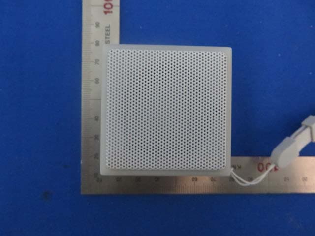
Y4N-IBO
Apr 21, 2015IBO Bluetooth speaker
Equipment Class
DSS - Part 15 Spread Spectrum Transmitter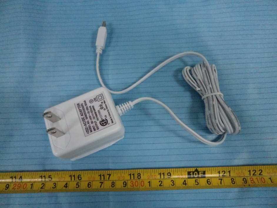
Y4N70208R
Feb 10, 2013MobiCam DXR Touch Wireless Monitoring System
Equipment Class
DSS - Part 15 Spread Spectrum Transmitter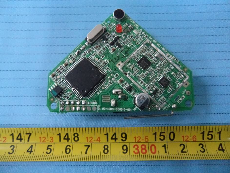
Y4N-70290T
Jan 12, 2012Pure Sounds Wireless Audio Monitor (Transmitter Unit)
Equipment Class
DSS - Part 15 Spread Spectrum Transmitter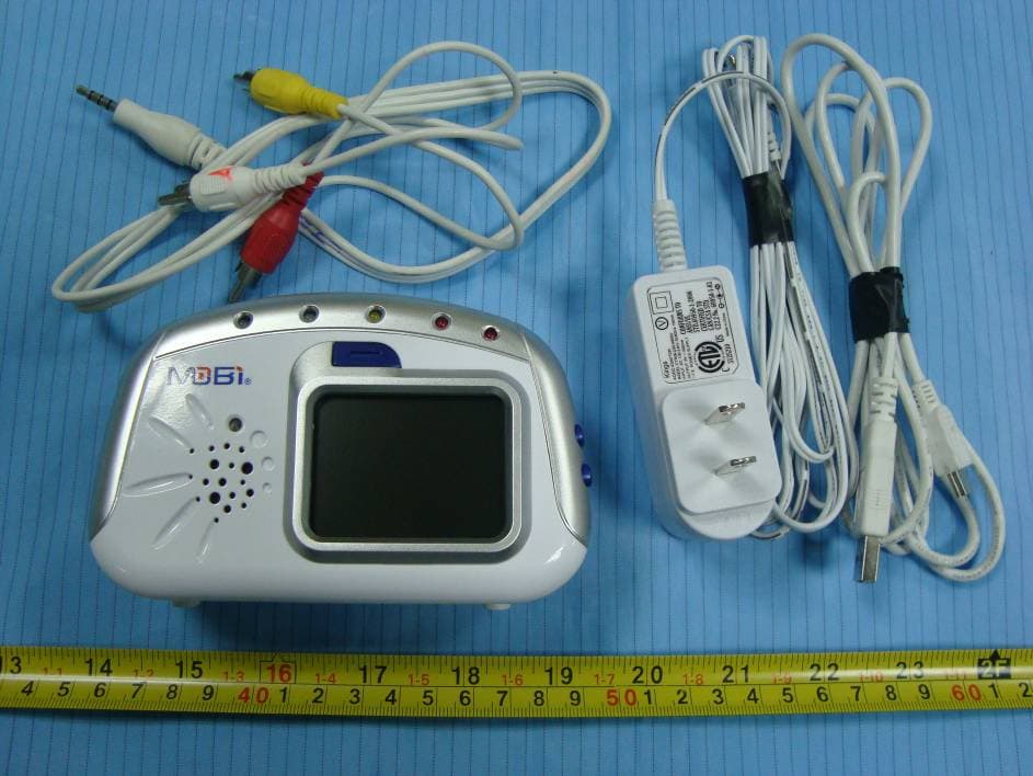
Y4N70055R
Feb 20, 2011Digital Video Baby Monitor
Equipment Class
DSS - Part 15 Spread Spectrum Transmitter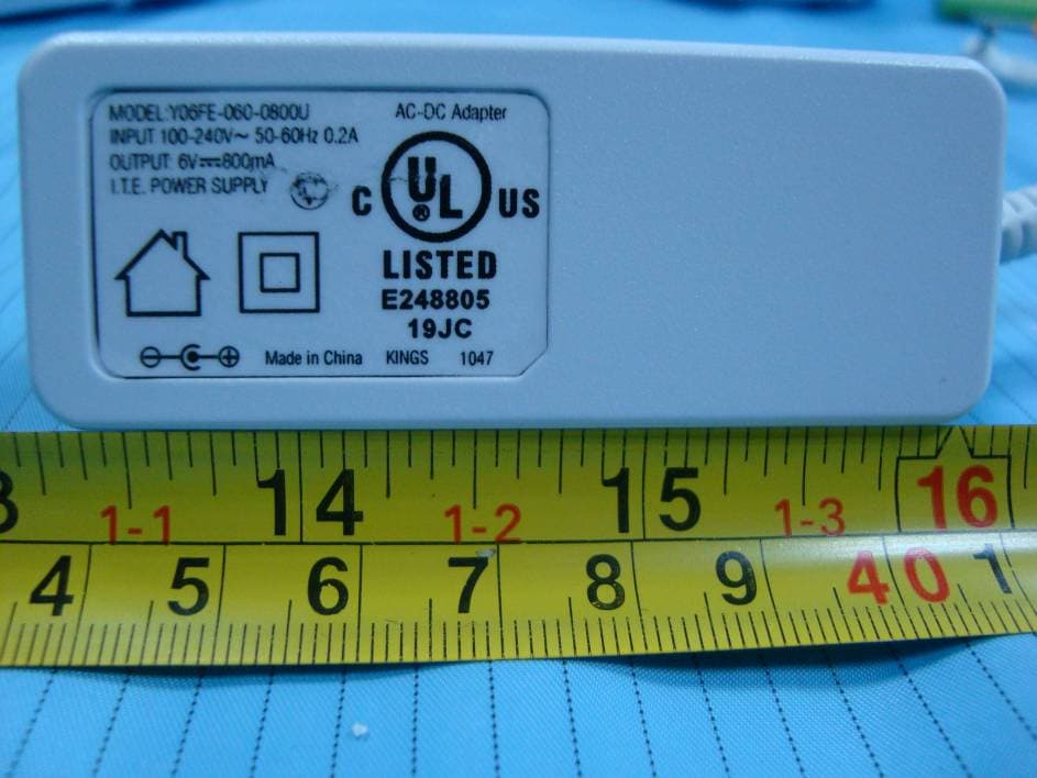
Y4N70055T
Feb 20, 2011Digital Video Baby Monitor
Equipment Class
DSS - Part 15 Spread Spectrum Transmitter