Y7J5094B01Keypad RF with Calculator
Canon Electronic Business Machines (H.K.) Co., Ltd.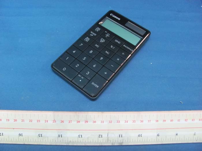
Click to zoom
Application Details
- Equipment Class
- DXX - Part 15 Low Power Communication Device Transmitter
- Date of Grant
- Aug 11, 2011
- Application Purpose
- Original Equipment
- Date of Application
- Aug 10, 2011
- Equipment Note
- Keypad RF with Calculator
- Frequency Range
- 2415.00000000 - 2470.00000000
- Country
- Hong Kong
Documents & Files
Document Text
Text extracted from the exhibit documents filed with the FCC. Open a document above to read the original.
Users Manual
2 Press the key. NOTE: The icon on the front display should be flashing. If not, press the key again. CALCULATOR MODE AND KEYPAD MODE When RF connected, this Calculator Keypad has 2 modes -- Calculator Mode (CAL) and Keypad Mode (KP). Switch between Calculator and Keypad Mode JTo switch between Calculator and Keypad mode, simply press the key. Calculator Mode (with RF connection) JThe calculator performs normal 10-digit calculator operations. JSend calculation results or display contents to a computer by pressing SEND . • You cannot perform a send operation while the E (Error) indicator is shown on the Calculator Keypad display. • The SEND key is disabled when the calculator is not RF connected. Keypad Mode (with RF connection) JInput the following to a computer directly: Numbers 0-9+ – ×÷ Auto Power Off and Wake-up JCalculator Only, NO RF Connection • The device will automatically power off after approximately 7 minutes of inactivity. Press the key to turn on the device. JCAL and KP Modes, with RF Connection • The RF connection will be disconnected after approximately 30 minutes of inactivity (the display will reset to “0”). The device will function the same as “Calculator Only, NO RF Connection”. Press to re-activate the RF connection. • After the RF connection is disconnected, the device will automatically power off after an additional 7 minutes of inactivity. Press and then to turn on the device and re-activate the RF connection. Power-low Indicator JWhen the display is dim or the icon appears, RF connection will not function. Replace the batteries to avoid running out of power unexpectedly. Keypad Lock (with RF connection) JPress the key and hold for 3 seconds to lock. JTo unlock, press the key and hold for 3 seconds. Power-low display Keypad locked display Radio Frequency Calculator Keypad / Teclado Calculadora Radio Frecuencia ●When finished using the calculator with a computer, remove the dongle from the computer and replace it in the slot on the back of the device. ●When using with a different computer, please connect again with the initial setup. ●The RF icon will remain on (solid, not flashing) when the Calculator Keypad is successfully connected to your computer. ●RF connection requires battery power to function properly. ●When RF connection is off, calculator functions can be used without batteries (powered by solar panel). USAGE TIPS USER GUIDE / GUIA DE USARIO PRINTED IN CHINA / IMPRESO EN CHINA ENGLISH IMPORTANT: READ BEFORE USE Please read the following instructions and safety precautions before using the Calculator Keypad. Keep this sheet on hand for future reference. THIS DEVICE IS WINDOWS AND MACINTOSH COMPATIBLE. Be sure to plug in the Radio Frequency (RF) dongle before connecting the Calculator Keypad to your computer. Hardware : Windows based PC x86 / x64 or above, Intel-based Mac Operating Windows ® XP (SP2 or above) or Windows Vista ® or Windows ® 7 System : Mac OS ® X 10.4 ~ 10.6 SYSTEM REQUIREMENTS ●Keep the batteries out of reach of children. ●Never expose batteries to high temperatures, direct heat, or dispose by incineration. ●Do not mix new and old batteries or batteries of different types. ●Do not allow metal objects to touch the battery terminals on the device; they can become hot and cause burns. ●Remove the batteries if they are worn out or have been stored for an extended period of time. ●Always remove old, weak, or worn out batteries promptly and recycle or dispose of them in accordance with Federal, State, and Local regulations. ●If a battery leaks, remove all batteries, taking care to keep the leaked fluid from touching your skin or clothes. If fluid from the battery comes into contact with skin or clothes, flush skin with water immediately. BATTERY CAUTION ! Model : X Mark I Keypad RF Power Source : AAA-size Alkaline batteries x 2 Operating Temperature : 0ºC to 40ºC (30ºF to 104ºF) Dimension : 155mm (L) x 86mm (W) x 20mm (H) 1-7/64” (L) x 3-25/64” (A) x 25/32” (A) DEVICE SPECIFICATIONS Frequency : 2.4 GHz frequency range Connection Range : The operating range is up to 10 meters (32.8 feet) NOTE : Connection range is affected by many factors, such as nearby metallic objects and the relative positioning of the device and the receiver. RADIO FREQUENCY SPECIFICATIONS NOTE: All specifications are subject to change without notice. ●Never continue to use the Calculator Keypad if it starts to smoke, emits a strange odor, or emits heat. Continued use of the calculator under such conditions creates the danger of fire and electric shock. ●When cleaning the Calculator Keypad, do not use a damp cloth or volatile liquid such as paint thinner; instead, use only a soft, dry cloth. ●Never dispose of the Calculator Keypad improperly (such as burning), which can lead to personal injury or harm. You should dispose of this product in accordance with Federal, State, and Local regulations. HANDLING AND CARE ▪Power on ▪Clear all display | Keypad lock / unlock ▪Re-connect the RF connection ▪Clear last input entered | Clear all input (CAL mode only) ▪Escape the input (KP mode only) ▪Switch between Calculator Mode or Keypad Mode ▪Backspace in Keypad mode; in Calculator mode shifts each digit of the displayed numerical value and clears the last significant digit ▪Send calculation results or display contents to computer (CAL mode with RF Connection) ▪Perform percentage add-on and discount calculation. (CAL mode only) ▪Execute calculation (CAL mode only) ▪Enter Key -- Confirm the input (KP mode only) ▪Set the number of digits displayed in calculation after the decimal point ▪Press and then press and hold , the display will change in the sequence of F 0 2 3 F (CAL mode only) ▪F represents a floating decimal point WAKE UP KEY INDEX © CANON ELECTRONIC BUSINESS MACHINES (H.K.) CO., LTD. 2011 Set-up may vary slightly depending on the computer. Instructions provided should work universally on Windows ® XP, Windows Vista ® , Windows ® 7, and Macintosh. 1. Remove the battery cover from…
Text truncated - open the document above for the full version.
Block Diagram
MCU SH67L19A LCD display Calculator Key Board Wake up key X Mark I Keypad RF 2.4G Block Diagram RF controller LSI (SH68F 091) 2011- 5 - 20 RF IC (ARF2 496 K ) Cal PCB Main PCB 2.4G RF Block Diagram
Cover Letter(s)
CAmSTT CANON ELECTRONTC BUSTNESS MACHTNES (H.K.) CO., LTD. 17|F.,'lower One, Ever Gain Plaza, 82-100 Container Port Road, Kwai Chung, New Teritories, Hong Kong. Phone: (852) 2305-8400 "1, an officer of Canon Electronic Business Machines (H.K.) Co., Ltd. do hereby authorize Intertek Testing Services (Mr. Terry Chan) to act on our behalf in front of the Federal Communications Commission with respect to all matters relating to certification of equipment under Part 15 and Part 18 of the FCC Rules until further notice." I further certify that no party (as defined in 51.2002(b) of CFR 47 , 2004) to this application, including myself, is subject to a denial of federal benefits, that includes FCC benefits, pursuant to Section 5301 of the Anti-Drug Abuse Act of 1988, 21 U.S.C.,862. Dated this 21 day of February,2011 Ronald Chan Printed Name Director Title Remark: The person who signs this authorization letter must be the grantee contact of record in the Grantee Code data base. Signature I I Nov 2010
Cover Letter(s)
Canon CANON ELECTRONIC BUSINESS MACHINES (H.K.) CO., LTD. 17lF., Tower One, Ever Gain Plaza, 82-100 Container Port Road, Kwai Chung, New Territories, Hong Kong. PHONE: (8s2) 230s-8400 Attention: Application Examiner Re: Request for confidentiality Applicant: fCanon Electronic Business Machines (H.K.) Co., Ltd.l FCC ID: [Y7J5 09 3 B 0 ]1, lYTJs 5 6 5 B 0 Il, [Y7J 5 09 4 B 0 t], [y 7 J s 0 9 4 B 0 I -D] To whom it may concern, Short-term ConfidentÍality Request is hereby submitted by lCanon Electronic Business Machines (H.K.) Co., Ltd.l iowithhold from public review for a period of 45 days from the date of the Grant of Equipment Authorization and prior to marketing, certain portions of the application for equipment certification for the referenced FCC identifiers. This request for confidentiality is made pursuant to 47 CFR 0.457(d) of the FCC Rules. In particular, the following sections of the application are' to be kept confidèntial for a period of 45 days from the date of Authoization: lSelect one or more of items below that are not selected in the list qbove, as appropriatel ¡ Schematics ¡ Detailed Block diagrams o DetailedOperational,/FunctionalDescription ¡ Test setup photos ¡ External photos o Internal photos . User manual Rationale for request for confidentiality: fCanon Electronic Business Machines (H.K.) Co., Ltd.l has invested considerable time and materials in research and development to produce the referenced product. Short term confidentiality.' Disclosure of the short-term confidential portions of this application during the period of importation and/or distribution would reveal key aspects of proprietary technology to competitors and diminish the value of our investment in research and development. Canon Electronic Business Machines (H.K.) Co., Ltd.
External Photos
INTERTEK TESTING SERVICE Report No.: HK11060153-4 FCC ID: Y7J5094B01 Equipment Photographs Model : X Mark I Keypad RF (External)
Internal Photos
INTERTEK TESTING SERVICE Report No.: HK11060153-4 FCC ID: Y7J5094B01 Equipment Photographs Model : X Mark I Keypad RF (Internal) INTERTEK TESTING SERVICE Report No.: HK11060153-4 FCC ID: Y7J5094B01 Equipment Photographs Model : X Mark I Keypad RF (Internal) INTERTEK TESTING SERVICE Report No.: HK11060153-4 FCC ID: Y7J5094B01 Equipment Photographs Model : X Mark I Keypad RF (Internal) INTERTEK TESTING SERVICE Report No.: HK11060153-4 FCC ID: Y7J5094B01 Equipment Photographs Model : X Mark I Keypad RF (Internal) INTERTEK TESTING SERVICE Report No.: HK11060153-4 FCC ID: Y7J5094B01 Equipment Photographs Model : X Mark I Keypad RF (Internal) INTERTEK TESTING SERVICE Report No.: HK11060153-4 FCC ID: Y7J5094B01 Equipment Photographs Model : X Mark I Keypad RF (Internal)
Operational Description
FCC ID: Y7J5094B01 Technical Description: The Equipment Under test (EUT) is a 2.4GHz Transceiver for a wireless calculator/ numeric keypad, which is operating at 2415 to 2470MHz with 1MHz channel spacing. The EUT is energized by either two AAA batteries or solar energy. The main function of the EUT is used to transmit the 2.4GHz GFSK modulation signal to the USB dongle for data transfer. The functions of main ICs are mentioned as below; 1) U1 acts as 2.4GHz RF chip. 2) U2 acts as MCU for RF controller. 3) IC1 acts as Micro-controller with LCD driver Antenna Used: Patch antenna has been used.
Operational Description
ARF2496K 2.4GHz RF Single Chip Transceiver The above information is the exclusive intellectual property of AlfaPlus Semiconductor and shall not be disclosed, distributed or reproduced without permission from AlfaPlus Semiconductor. - 1 - Version 1.67 Data Sheet AlfaPlus Semiconductor Inc. General Description The ARF2496K is a low-power, high-integrated single chip RF transceiver using 0.18μm mixed-mode CMOS process optimized for ISM 2.4GHz wireless systems. The ARF2496K contains receiver, transmitter, voltage-controlled oscillator (VCO) and phase-locked loop (PLL). The device is expressly designed for low power consumption. Specific expertise has been applied to save current consumption and thus to extend the battery life, which is of most importance to the portable wireless consumer applications. Power saving mode has also been implemented to further reduce the power consumption. The receiver contains a low-noise amplifier (LNA), a high-frequency mixer, a received signal strength indicator (RSSI), a channel select filter, a limiting amplifier, a demodulator and a data slicer with clock recovery. Current consumption of receive mode is 18mA and transmit mode is 10.5mA at –5dBm output. Features z 2.4GHz GFSK RF transceiver z Operates in unlicensed worldwide Industrial, Science and Medical (ISM) band (2.400GHz ~ 2.527GHz) z Sensitively up to –93 dBm z Output power up to 0 dBm z Low-noise amplifier, power amplifier, modern and data slicer/recovery on chip z Low operation voltage from 1.9V to 3.6V z Low current consumption, 8.2mA@-20dBm at TX mode and 18mA at RX mode z Programmable 250kbps/1Mbps transfer bit-rate z Configurable preamble, scramble, source address, destination address and CRC generation z Programmable data payload length from 1-byte to 32-byte z 3-wire SPI interface for device configuration z Complete RSSI function on chip z Operation temperature range from –40 °C to +85 °C z Compact 24-pin QFN 4x4 mm package Applications z Wireless Mouse, Presenters, Keyboards and Gamepad z Wireless VOIP and Headsets z Remote Controls z Toys z Home Automation z Consumer Electronics The above information is the exclusive intellectual property of AlfaPlus Semiconductor and shall not be disclosed, distributed or reproduced without permission from AlfaPlus Semiconductor. - 2 - 2 Version 1.67 Data Sheet AlfaPlus Semiconductor Inc. Table of Contents General Description .......................................................... 1 Features............................................................................. 1 Applications ...................................................................... 1 Table of Contents .............................................................. 2 Pin Configuration.............................................................. 3 Block Diagram.................................................................. 3 Electrical Specifications ................................................... 4 Absolute Maximum Ratings ..................................... 4 Recommend Operating Conditions ........................... 4 DC Electrical Characteristics .................................... 4 AC Electrical Characteristics .................................... 4 Function Description......................................................... 5 Internal State and Operation Mode ........................... 5 Power-Down Mode........................................... 5 Power-Saving Mode.......................................... 5 Stand-By Mode.................................................. 6 SPI-Access Mode.............................................. 6 Active Mode...................................................... 6 Operation Mode and Pin Behavior................... 6 Data Transfer Modes................................................. 6 RX/Direct Mode................................................ 6 RX/Burst Mode.................................................. 7 TX/Direct Mode................................................ 7 TX/Burst Mode.................................................. 8 TX/Multi-Burst Mode........................................ 8 Timing of TRRDY to TRRDY at RX Mode......... 9 Advantage by Using Burst Mode...................... 9 Packet Format ........................................................... 9 Preamble........................................................... 9 Destination Address.......................................... 9 Reserved.......................................................... 10 Source Address................................................ 10 Data................................................................ 10 CRC................................................................. 10 SPI Interface ........................................................... 10 SPI Interface Pins........................................... 10 SPI Packet Format.......................................... 10 Timing of SPI Read-Access............................. 11 Timing of SPI Write-Access............................. 11 Timing of TRRDY to SPIEN............................ 11 RSSI Function......................................................... 11 Output Power Ramp-Up/Down Function................ 11 PLL Pre-Turn-On Time ........................................... 12 Antenna Interface.................................................... 12 Global Clock ........................................................... 12 Power Supply.......................................................... 12 Device Registers ............................................................. 13 Register List and Index................................... 13 T/R and Channel Index (0x00)........................ 13 Crystal Frequency and Output Power (0x01).13 Data Function Control (0x02)........................ 14 RSSI Function Control (0x03)......................... 14 RSSI Value (0x04)........................................... 14 Data Format Control (0x05).........................…
Text truncated - open the document above for the full version.
Schematics
11 22 33 44 55 66 77 88 D D C C B B A A Ti tle Nu mb er Revis io n Size A3 Date: 2011-7-14 Sheet of Fil e: E: \20 11 \..\ X_MARK_ Pad_T X(2 011 06 21 )FCC.SCH Drawn By: C1222 pF C1922 P C2022 P C91p F Y2 16 MHz R31M VBA T1 LOGITECH X_MARK_PAD_TX L13. 9nH L2 5. 6nH C21p F 1. 5Vx 2 A AA C2147 uF C140. 1uF C131u F C151u F C101u F C722 pF R256 K C110 4 R110 K VBA T C30. 1uF L410 nH WAKEUPPA0 CLKDA TA CONNECT 12345678910 COM1Header 10 VBA T C160. 1uF VCC TRRDY 1 TRSCLK 2 TRSDA T 3 SPIEN 4 VCCD 5 GN DD 6 VD DD 7 XO UT 8 XI N 9 PSB 10 GN DV CO 11 VCC VCO 12 VD DRF 13 AN T1 14 AN T2 15 VSSRF 16 VCCRF 17 GN DIF 18 RSSI 19 IREF 20 TRINT 21 DRSSI 22 T06 23 T07 24 U1ARF24 96 K E1 An tenn a L312 nH C181u F C1710 uF VCC VCC_RF VCC_RF VCC _RF PSB DRSSI L547 uH C510 0n F C1147 uF C410 0n F J1 VCC J6 GN D J2 TD O J3 TCK J5 TD I J4 TMS VCC PROGRAM PIN TCKTD ITMS TDO TD OTCKTMSTD I CHECKPA0 C612 PC812 P Y16MH z VCC RESET WAK EUP P35 1 P36 2 P37 3 RSTB 4 P00 5 P01 6 P02 7 P03 8 P04 9 P05 10 P06 11 P07 12 GN D 13 P10 14 P11 15 P12 16 P13 17 P14 18 P15 19 P16 20 P17 21 POLYFUSE NC P20 22 P21 23 P22 24 P23 25 GN D 26 P24 27 P25 28 P26 29 P27 30 P40 31 P41 32 P42 33 SOUT 34 AG ND 35 AG ND 35 LX 36 LX 36 VO UT 37 VO UT 37 GN D 38 VCC 39 VCC 39 OSCO 40 OSCI 41 GN D 42 GN D 42 VI N 43 P43 44 P44 45 P30 46 P31 47 P32 48 P33 49 P34 50 U2 SH68F091_DIE(50) S1TE ST Q1C1815 Q2C1815 R447 K R547 K R647 K C221u F D11SS5C1 VBA T R91M VBA T1 R1110 0K R120 D21N 58 19 Q4 C1815 R1410 0K R1310 0 Q3 APM23 17 R10 2M 1 2 34 ABCD 4 3 2 1 D CBA Title:Size: Drawing Name: Date:Drawn By: Check By: ConfiRm By: Revision: Sheet of A4 LOGITECH V2 Di Li 2011-05-25 1/1 X mark 1 K (RF) PD3/S30 1 PD2/S31 2 PD1/S32 3 PD0/S33 4 PC3/S34 5 PC2/S35 6 PC1/S36 7 PC0/S37 8 CX/S38 9 PA3 10 PA2 11 PA1 12 PA0 13 PB3 14 PB2 15 PB1 16 PB0 17 B0 65 VDD 18 OSC0 19 OSC1 20 OSCX0 21 OSCX1 22 B1 66 RESET 24 TESET 25 CPU1 26 CPU2 27 VP2 28 VP1 29 C1 30 C2 31 GND 23 C3 32 C4 33 C5 34 C6 35 S1 36 S2 37 S3 38 S4 39 S5 40 S6 41 S7 42 S8 43 S9 44 S10 45 S11 46 S12 47 S14 49 S15 50 S16 51 S17 52 S18 53 S19 54 S20 55 S21 56 PF3/S22 57 PF2/S23 58 PF1/S24 59 PF0/S25 60 PE3/S26 61 PE2/S27 62 PE1/S28 63 PE0/S29 64 S13 48 IC1 SH67L19A R162.32M R9 976K C10.1UC20.1U C30.1U C4 0.1U V15 PB0PB1PB2PB3PA0PA1PA2PA3S38PC0PD0PD1PD2PD3 PE0 PE1 PE2 PE3 S13 S14 S15 S16 S17 S18 S19 S20 S21 S22 S23 S24 S25 VOUT 5 NC 4 GND 2 CE 3 VDD 1 U1R1180N151B VBAT V15 K25 . K24+ K19 1 K21 2 K22 3 K20 - K26ON/AC K16 4 K17 5 K14 6 K18 X K15Send K10 7 K9 8 K11 9 K12 DIV K13 M-/= K2 %+/- K3 CAL/PC K4 BS K7 C/CI K8RM/CM K5Enter/= K6 M+/= PD3PE0PE1PA0 PB0 PB1 PB2 PB3 PC0 Vin 2 GND 3 Vout 1 U2 XC61CN2102PR VBAT PA3 V30 WAKEUP PA0 CLK DATA CHECKPA0CONNECT VBAT R12100KR13100K R14100KR15100K R647K R3 47K R447K R7100K PE2PE3PA2PA1PD0PD1PD2 C1C2C3C4C5S1S6S7S8S9S10S11S12S13S14S15S16S17S18S19S20S21S22S23S24S25S38 S12S6S7S8S9S10S11C1C2 C3C4S1 RESET V15 C5 R1 510K V15 R8 510K V15 C7 0.1U R10 100K R547K V30 NOTE1:OSC Freq R16 131KHz 262KHz 2.32M+/-1% 976K+/-1% 123456789 10 CON1FFC10 Wakeup K1Wakeup R2 100 R9 NOTE1 NOTE1 C6 4.7U/10V K27OFF Designator Part C80.1U 1 2 SOLAR1SC-1338I Q2C1815 Q1C1815 C5 1 C1 2 C2 3 C3 4 C4 5 S1 6 S5 7 S6 8 S7 9 S8 10 S9 11 S10 12 S11 13 S12 14 S13 15 S14 16 S15 17 S16 18 S17 19 S18 20 S19 21 S20 22 S21 23 S22 24 S23 25 S24 26 S25 27 S38 28 LCD1LCD28 1.2PH S5 S5 R171M Vin 3 Vss 2 Vout 1 U3XC61CN1002M V15 RESET D1 IN4148 C9 22uf/6.3V C50.1U option option option K36 RESET K23 0 VDB0034ATRH D2IN4148 D3 1SS15C1
Test Report
INTERTEK TESTING SERVICES Report No.: HK11060153-4 Sample No.: 1/2 (Keypad) Code: FCC15C_e / Effective Date: 20 Dec 2010 ( of ) Bandedge Plot – Pursuant to FCC Part 15 Section 15. 249 Requirement
Test Report
- The test report only allows to be revised within the retention period unless further standard or the requirement was noticed. - This report is for the exclusive use of Intertek's Client and is provided pursuant to the agreement between Intertek and its Client. Intertek's responsibility and liability are limited to the terms and conditions of the agreement. Intertek assumes no liability to any party, other than to the Client in accordance with the agreement, for any loss, expense or damage occasioned by the use of this report. Only the Client is authorized to permit copying or distribution of this report and then only in its entirety. Any use of the Intertek name or one of its marks for the sale or advertisement of the tested material, product or service must first be approved in writing by Intertek. The observations and test results in this report are relevant only to the sample tested. This report by itself does not imply that the material, product, or service is or has ever been under an Intertek certification program. Intertek Testing Services Hong Kong Ltd. 2/F., Garment Centre, 576 Castle Peak Road, Kowloon, Hong Kong. Tel: (852) 2173 8888 Fax: (852) 2785 5487 Website: www.hk.intertek-etlsemko.com TEST REPORT Report No.: HK11060153-4 Canon Electronic Business Machines (H.K.) Co., Ltd. Application For Certification (Original Grant) (FCC ID: Y7J5094B01) Transceiver Prepared and Checked by: Approved by: Signed On File Wong Kwok Yeung, Kenneth Lead Engineer Chan Chi Hung, Terry Assistant Supervisor Date: August 02, 2011 INTERTEK TESTING SERVICES Report No.: HK11060153-4 FCC ID: Y7J5094B01 i GENERAL INFORMATION Canon Electronic Business Machines (H.K.) Co., Ltd. BRAND NAME: Canon, MODEL: X Mark I Keypad RF FCC ID: Y7J5094B01 Grantee: Canon Electronic Business Machines (H.K.) Co., Ltd. Grantee Address: 17/F., Tower One, Ever Gain Plaza, 82-100 Container Port Road, Kwai Chung, N.T., Hong Kong. Contact Person: Mr. Ronald Chan Tel: 852-2305 8400 Fax: 852-2318 1719 e-mail: [email protected] Manufacturer: Canon Electronic Business Machines (H.K.) Co., Ltd. Manufacturer Address: 17/F., Tower One, Ever Gain Plaza, 82-100 Container Port Road, Kwai Chung, N.T., Hong Kong. Brand Name: Canon Model: X Mark I Keypad RF Type of EUT: Transceiver Description of EUT: Keypad RF with Calculator Serial Number: N/A FCC ID: Y7J5094B01 Date of Sample Submitted: June 02, 2011 Date of Test: July 28, 2011 Report No.: HK11060153-4 Report Date: August 02, 2011 Environmental Conditions: Temperature: +10 to 40°C Humidity: 10 to 90% INTERTEK TESTING SERVICES Report No.: HK11060153-4 FCC ID: Y7J5094B01 ii SUMMARY OF TEST RESULT Canon Electronic Business Machines (H.K.) Co., Ltd. BRAND NAME: Canon, MODEL: X Mark I Keypad RF FCC ID: Y7J5094B01 TEST SPECIFICATION REFERENCE RESULTS Maximum Peak Output Power 15.247(b), (c) / RSS-210 A8.4 N/A Hopping Channel Carrier Frequencies Separation 15.247(e) / RSS-210 A8.1 N/A 20dB Bandwidth of the Hopping Channel 15.247(a) / RSS-210 A8.1 N/A Number of Hopping Frequencies 15.247(e) / RSS-210 A8.1 N/A Average Time of Occupancy of Hopping Frequency 15.247(e) / RSS-210 A8.1 N/A Antenna Conducted Spurious Emissions 15.247(d) / RSS-210 A8.5 N/A Radiated Spurious Emissions 15.247(d) / RSS-210 A8.5 N/A RF Exposure Compliance 15.247(i) / RSS-Gen 5.6 N/A Transmitter Power Line Conducted Emissions 15.207 / RSS-Gen 7.2.4 N/A Transmitter Field Strength 15.227 / RSS-310 3.8 N/A Transmitter Field Strength 15.229 / RSS-210 A2.7 N/A Transmitter Field Strength, Bandwidth and Timing Requirement 15.231(a) / RSS-210 A1.1.1 N/A Transmitter Field Strength, Bandwidth and Timing Requirement 15.231(e) / RSS-210 A1.1.5 N/A Transmitter Field Strength and Bandwidth Requirement 15.239 / RSS-210 A2.8 N/A Transmitter Field Strength and Bandwidth Requirement 15.249 / RSS-210 A2.9 Pass Transmitter Field Strength and Bandwidth Requirement 15.235 / RSS-310 3.9 N/A Digital Device Radiated Emissions 15.109 / ICES-003 Pass Digital Device Conducted Emissions 15.107 / ICES-003 N/A Note: 1. The EUT uses a permanently attached antenna which, in accordance to section 15.203, is considered sufficient to comply with the pervisions of this section. 2. Pursuant to FCC part 15 Section 15.215(c), the 20 dB bandwidth of the emission was contained within the frequency band designated (mentioned as above) which the EUT operated. The effects, if any, from frequency sweeping, frequency hopping, other modulation techniques and frequency stability over excepted variations in temperature and supply voltage were considered. INTERTEK TESTING SERVICES Report No.: HK11060153-4 FCC ID: Y7J5094B01 iii Table of Contents 1.0 General Description................................................................................................1 1.1 Product Description................................................................................................1 1.2 Related Submittal(s) Grants.................................................................................1 1.3 Test Methodology...................................................................................................1 1.4 Test Facility.............................................................................................................1 2.0 System Test Configuration ....................................................................................2 2.1 Justification..............................................................................................................2 2.2 EUT Exercising Software......................................................................................3 2.3 Special Accessories................................................................................................2 2.4 Equipment Modification..........................................................................................2 2.5 Measurement Uncertainty......................................................................................2 2.6 Support Equipment…
Text truncated - open the document above for the full version.
Test Setup Photos
INTERTEK TESTING SERVICE Report No: HK11060153-4 FCC ID: Y7J5094B01 Configuration Photographs Worst-Case Radiated Emissions (Front View) Model : X Mark I Keypad RF INTERTEK TESTING SERVICE Report No: HK11060153-4 FCC ID: Y7J5094B01 Configuration Photographs Worst-Case Radiated Emissions (Back View) Model : X Mark I Keypad RF
Contact Information
Applicant
Chi Tat Leung(R&D Director)
Technical Contact
Intertek Testing Services Hong Kong LtdTerry Chan
[email protected]2173 8503
2/F Garment Centre · Kowloon · Hong Kong
Non-Technical Contact
Intertek Testing Services Hong Kong LtdTerry Chan
[email protected]2173 8503
Test Firm
Intertek Testing Services Hong Kong Ltd.Billy Chow
Technical Specifications
| # | Rule Parts | Frequency Range | Power Output |
|---|---|---|---|
| 1 | 15C | 2.42 GHz - 2.47 GHz | - |
Other Applications from Canon Electronic Business Machines (H.K.) Co., Ltd.
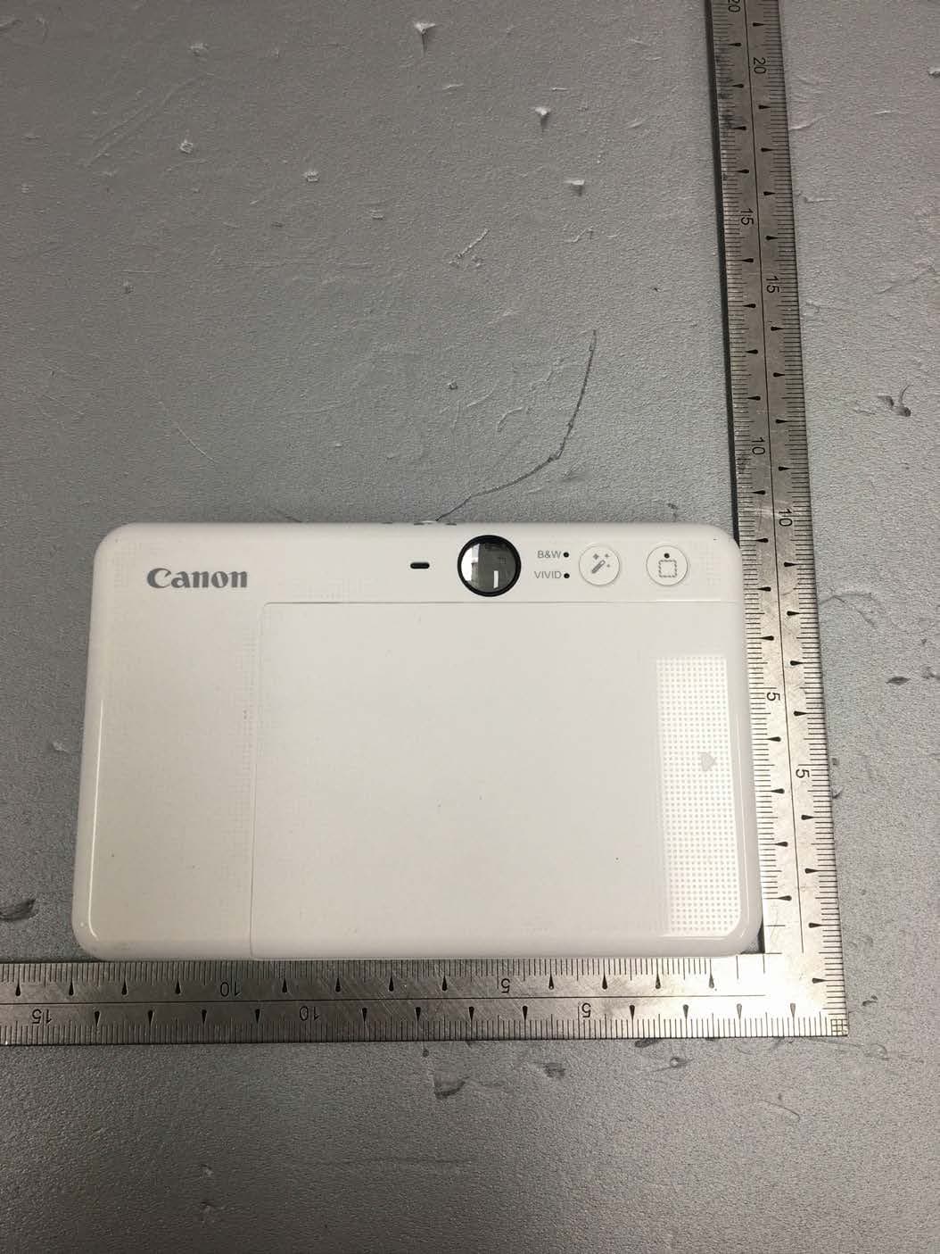
Y7J-PP2002
Mar 11, 2020Instant Camera Printer
Equipment Class
DTS - Digital Transmission System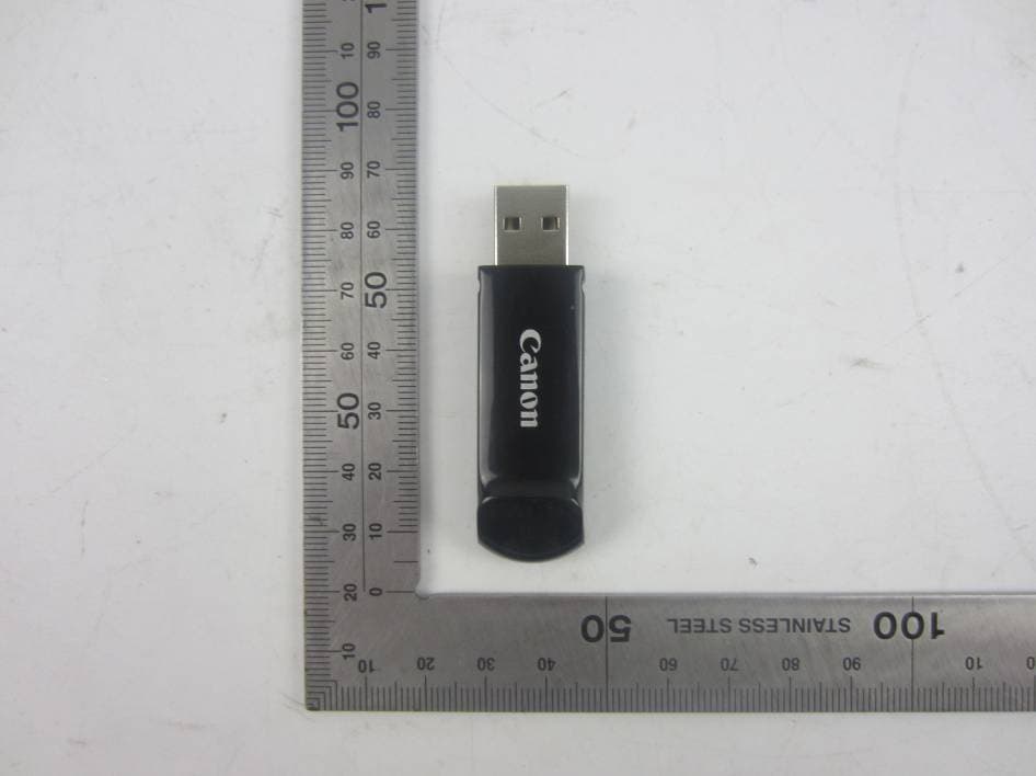
Y7J-PR100RR
Oct 25, 20152.4G wireless presenter (dongle)
Equipment Class
DXX - Part 15 Low Power Communication Device Transmitter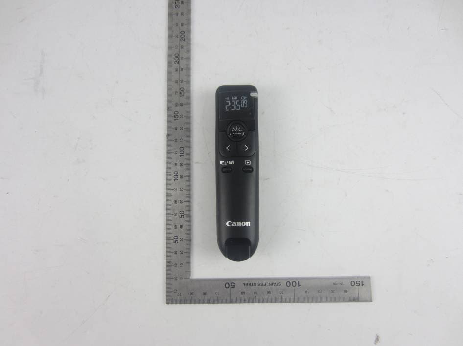
Y7J-PR100RT
Oct 22, 20152.4G wireless presenter (device)
Equipment Class
DXX - Part 15 Low Power Communication Device Transmitter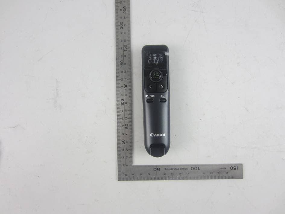
Y7J-PR10GT
Oct 22, 20152.4G wireless presenter (device)
Equipment Class
DXX - Part 15 Low Power Communication Device Transmitter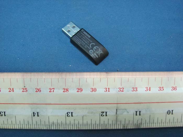
Y7J5094B01-D
Aug 10, 2011Keypad RF with Calculator (Dongle)
Equipment Class
DXX - Part 15 Low Power Communication Device Transmitter