Z64-CC256XMODNKITCC2564 Module EM Board
Texas Instruments Incorporated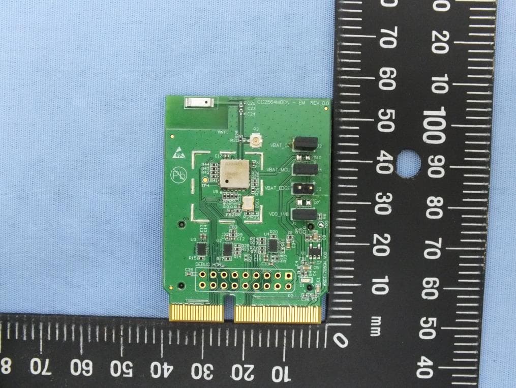
Click to zoom
Application Details
- Equipment Class
- DSS - Part 15 Spread Spectrum Transmitter
- Date of Grant
- Mar 25, 2014
- Application Purpose
- Original Equipment
- Date of Application
- Mar 25, 2014
- Equipment Note
- CC2564 Module EM Board
- Frequency Range
- 2402.00000000 - 2480.00000000
- Country
- United States
Documents & Files
Document Text
Text extracted from the exhibit documents filed with the FCC. Open a document above to read the original.
Users Manual
AMPAK Technology Inc. Advanced Module Packaging Solution 正基科技股份有限公司 CC2564MODNEM User manual Revision History Date Revision Content Revised By Version 2013/12/24 Initial released Rue 1.0 AMPAK Technology Inc. www.ampak.com.tw Proprietary & Confidential Information i Doc. NO: Contents 1. CC2564MODN evaluation module introduction ....................................................... 1 2. PIN Description/ Operating Ratings/ Operating temperature ................................. 3 3. Federal Communication Commission Interference Statement ................................ 6 4. Industry Canada statement ......................................................................................... 7 AMPAK Technology Inc. www.ampak.com.tw Proprietary & Confidential Information i Doc. NO: 1. CC2564MODN evaluation module introduction CC2564MODN evaluation module (EM) likes as figure1. That is designed for Bluetooth 2.1+EDR application. The bottom views like as figure2. It is also designed for TI’s MSP430 experimenter board. It is subject to provide a convenient environment for customer’s verification on Bluetooth function. There are controller pins on evaluation board which describes as below. Figure1. Top view of CC2564MODNEM AMPAK Technology Inc. www.ampak.com.tw Proprietary & Confidential Information Doc. NO: 1 Figure2. Bottom view of CC2564MODNEM Interface highlights: 1. U5: CC2564MODN SIP module. 2. P3: U.FL connector let RF signal in/out path, which R30 need tie on 0ohm. 3. J4: V B AT_MCU: 3V3 for main system power path form RF2. 4. J3: VBAT_EDGE: 3V3 for main system power path form P2 5. J2&R10: VBAT_CC: 3V3 for CC2564MODN main power 6. J1&R7: VDO_1V8: V8 for system IO level path 7. RF1&RF2&P2: For TI’s experimenter board IO used. AMPAK Technology Inc. www.ampak.com.tw Proprietary & Confidential Information Doc. NO: 2 2. PIN Description/ Operating Ratings/ Operating temperature 2.1 PIN Description Connector No. Pin Name Def. Dir. Description of Options (Common) RF1 1,19 GND Connect to ground 3 HCI_CTS_3V3 I HCI UART clear-to-send 5 SLOW_CLK_3V3 I 32.768-KHz clock in 7 HCI_RX_3V3 I HCI UART data receive 9 HCI_TX_3V3 O HCI UART data transmit others Not connected RF2 2 GND Connect to ground 7,9 +3V3 I Connect to +3.3V 8 AUD_OUT_3V3 O PCM data output 10 AUD_IN_3V3 I PCM data input 11 AUD_FSYNC_3V3 I/O PCM frame synch 17 AUD_CLK_3V3 I/O PCM clock 18 HCI_RTS_3V3 O HCI UART request-to-send 19 nSHUTD_3V3 I Shutdown input (active low) others Not connected AMPAK Technology Inc. www.ampak.com.tw Proprietary & Confidential Information Doc. NO: 3 Connector No. Pin Name Def. Dir. Description of Options (Common) P2 1 SLOW_CLK_EDGE I 32.768-KHz clock in 8 1V8_IN I Connect to +1.8V 52 AUD_CLK_1V8 I/O PCM clock 54 AUD_FSYNC_1V8 I/O PCM frame synch 56 AUD_IN_1V8 I PCM data input 58 AUD_OUT_1V8 O PCM data output 66 HCI_TX_1V8 O HCI UART data transmit 68 HCI_RX_1V8 I HCI UART data receive 70 HCI_CTS_1V8 I HCI UART clear-to-send 72 HCI_RTS_1V8 O HCI UART request-to-send 76 TX_DEBUG_1V8 I DEBUG port use 89 nSHUTDOWN_1V8 I Shutdown input (active low) 3, 9, 19, 37, 47, 63, 77, 83, 87, 95, 97, GND Connect to ground 2, 6, 18, 22, 42, 60, 64, 92 GND Connect to ground others Not connected AMPAK Technology Inc. www.ampak.com.tw Proprietary & Confidential Information Doc. NO: 4 2.2 Operating Ratings Test conditions: At room temperature 25°C Description Min. Typ. Max. Unit Input supply Voltage 2.2 3.3 4.85.5 V 2.3 Operating temperature Operating temperature -40°C to 85°C AMPAK Technology Inc. www.ampak.com.tw Proprietary & Confidential Information Doc. NO: 5 3. Federal Communication Commission Interference Statement This equipment has been tested and found to comply with the limits for a Class B digital device, pursuant to Part 15 of the FCC Rules. These limits are designed to provide reasonable protection against harmful interference in a residential installation. This equipment generates, uses and can radiate radio frequency energy and, if not installed and used in accordance with the instructions, may cause harmful interference to radio communications. However, there is no guarantee that interference will not occur in a particular installation. If this equipment does cause harmful interference to radio or television reception, which can be determined by turning the equipment off and on, the user is encouraged to try to correct the interference by one of the following measures: - Reorient or relocate the receiving antenna. - Increase the separation between the equipment and receiver. - Connect the equipment into an outlet on a circuit different from that to which the receiver is connected. - Consult the dealer or an experienced radio/TV technician for help. FCC Caution: Any changes or modifications not expressly approved by the party responsible for compliance could void the user's authority to operate this equipment. This device complies with Part 15 of the FCC Rules. Operation is subject to the following two conditions: (1) This device may not cause harmful interference, and (2) this device must accept any interference received, including interference that may cause undesired operation. IMPORTANT NOTE: FCC Radiation Exposure Statement: This equipment complies with FCC radiation exposure limits set forth for an uncontrolled environment. This equipment should be installed and operated with minimum distance 20cm between the radiator & your body. This transmitter must not be co-located or operating in conjunction with any other antenna or transmitter. AMPAK Technology Inc. www.ampak.com.tw Proprietary & Confidential Information Doc. NO: 6 4. Industry Canada statement This device complies with Industry Canada licence-exempt RSS standard(s). Operation is subject to the following two conditions: (1) this device may not cause interference, and (2) this device must accept any interference, including interference that may cause undesired operation of the device. Le présent appareil est conforme aux CNR d'Industrie Canada applicab…
Text truncated - open the document above for the full version.
External Photos
Project No.: EP3D0401 Page No. : 1 of 5 Photographs of EUT Project No.: EP3D0401 Page No. : 2 of 5
Internal Photos
Project No.: EP3D0401 Page No. : 3 of 5 Project No.: EP3D0401 Page No. : 4 of 5 Project No.: EP3D0401 Page No. : 5 of 5
RF Exposure Info
Report No.: FA3D0401 Page : 1 of 5 Report Version: Rev. 01 FCC RF Exposure Report FCC ID : Z64-CC256XMODNKIT Equipment : CC2564 Module EM Board Model No. : CC2564MODNEM Brand Name : Texas Instruments Applicant : Texas Instruments Inc Address : 12500 TI Blvd, Dallas USA 75243 Standard : 47 CFR FCC Part 2.1091 Received Date : Dec. 04, 2013 Tested Date : Dec. 18, 2013 ~ Feb. 27, 2014 We, International Certification Corp., would like to declare that the tested sample has been evaluated and in compliance with the requirement of the above standards. The test results contained in this report refer exclusively to the product. It may be duplicated completely for legal use with the approval of the applicant. It shall not be reproduced except in full without the written approval of our laboratory. Approved & Reviewed by: Gary Chang / Manager Ty: XXX Report No.: FA3D0401 Page : 2 of 5 Report Version: Rev. 01 Table of Contents 1 MPE EVALUATION OF MOBILE DEVICES ......................................................................................... 4 1.1 LIMITS FOR GENERAL POPULATION/UNCONTROLLED EXPOSURE............................................. 4 1.2 MPE EVALUATION FORMULA ............................................................................................................. 4 1.3 MPE EVALUATION RESULTS .............................................................................................................. 4 2 TEST LABORATORY INFORMATION ................................................................................................. 5 Report No.: FA3D0401 Page : 3 of 5 Report Version: Rev. 01 Release Record Report No. Version Description Issued Date FA3D0401 Rev. 01 Initial issue Mar. 18, 2014 Report No.: FA3D0401 Page : 4 of 5 Report Version: Rev. 01 1 MPE EVALUATION OF MOBILE DEVICES Human exposure to RF emissions from mobile devices (47 CFR §2.1091) may be evaluated based on the MPE limits adopted by the FCC for electric and magnetic field strength and/or power density, as appropriate, since exposures are assumed to occur at distances of 20 cm or more from persons. 1.1 LIMITS FOR GENERAL POPULATION/UNCONTROLLED EXPOSURE Frequency Range (MHz) Power Density (mW /cm 2 ) Averaging Time (minutes) 300~1500 F/1500 30 1500~100000 1.0 30 1.2 MPE EVALUATION FORMULA Pd = 2 **4RPi Pt Where Pd= Power density in mW/cm 2 Pt= EIRP in mW Pi= 3.1416 R= Measurement distance 1.3 MPE EVALUATION RESULTS Frequency Range (MHz) Maximum Conducted Power (dBm) Antenna Gain (dBi) Distance (cm) Power Density (mW/cm 2 ) Limit (mW/cm 2 ) 2402~2480 (BT EDR) 12.97 -1.38 20 0.003 1 2402~2480 (BT LE) 11.25 -1.38 20 0.002 1 Report No.: FA3D0401 Page : 5 of 5 Report Version: Rev. 01 2 Test laboratory information Established in 2012, ICC provides foremost EMC & RF Testing and advisory consultation services by our skilled engineers and technicians. Our services employ a wide variety of advanced edge test equipment and one of the widest certification extents in the business. International Certification Corp, it is our definitive objective is to institute long term, trust-based associations with our clients. The expectation we set up with our clients is based on outstanding service, practical expertise and devotion to a certified value structure. Our passion is to grant our clients with best EMC / RF services by oriented knowledgeable and accommodating staff. Our Test sites are located at Linkou District and Kwei Shan Hsiang. Location map can be found on our website http://www.icertifi.com.tw. Linkou Kwei Shan Tel: 886-2-2601-1640 Tel: 886-3-271-8666 No. 30-2, Ding Fwu Tsuen, Lin Kou District, New Taipei City, Taiwan, R.O.C. No. 3-1, Lane 6, Wen San 3rd St., Kwei Shan Hsiang, Tao Yuan Hsien 333, Taiwan, R.O.C. If you have any suggestion, please feel free to contact us as below information Tel: 886-3-271-8666 Fax: 886-3-318-0155 Email: [email protected] ══END══
Test Report
Report No.: FR3D0401AD Page : 1 of 47 Report Version: Rev. 01 FCC Test Report FCC ID : Z64-CC256XMODNKIT Equipment : CC2564 Module EM Board Model No. : CC2564MODNEM Brand Name : Texas Instruments Applicant : Texas Instruments Inc Address : 12500 TI Blvd, Dallas USA 75243 Standard : 47 CFR FCC Part 15.247 Received Date : Dec. 04, 2013 Tested Date : Dec. 12, 2013 ~ Feb. 27, 2014 We, International Certification Corp., would like to declare that the tested sample has been evaluated and in compliance with the requirement of the above standards. The test results contained in this report refer exclusively to the product. It may be duplicated completely for legal use with the approval of the applicant. It shall not be reproduced except in full without the written approval of our laboratory. Approved & Reviewed by: Gary Chang / Manager Ty: XXX Report No.: FR3D0401AD Page : 2 of 47 Report Version: Rev. 01 Table of Contents 1 GENERAL DESCRIPTION .................................................................................................................... 5 1.1 Information .............................................................................................................................................. 5 1.2 Local Support Equipment List ................................................................................................................ 7 1.3 Test Setup Chart .................................................................................................................................... 7 1.4 The Equipment List ................................................................................................................................ 8 1.5 Test Standards ....................................................................................................................................... 9 1.6 Measurement Uncertainty .................................................................................................................... 10 2 TEST CONFIGURATION ..................................................................................................................... 11 2.1 Testing Condition ................................................................................................................................. 11 2.2 The Worst Test Modes and Channel Details ....................................................................................... 11 3 TRANSMITTER TEST RESULTS ........................................................................................................ 12 3.1 Conducted Emissions ........................................................................................................................... 12 3.2 Unwanted Emissions into Restricted Frequency Bands ...................................................................... 15 3.3 Emissions in non-restricted frequency bands ...................................................................................... 31 3.4 Conducted Output Power ..................................................................................................................... 36 3.5 Number of Hopping Frequency ............................................................................................................ 38 3.6 20dB and Occupied Bandwidth ............................................................................................................ 40 3.7 Channel Separation .............................................................................................................................. 42 3.8 Number of Dwell Time .......................................................................................................................... 44 4 TEST LABORATORY INFORMATION ............................................................................................... 47 Report No.: FR3D0401AD Page : 3 of 47 Report Version: Rev. 01 Release Record Report No. Version Description Issued Date FR3D0401AD Rev. 01 Initial issue Mar. 18, 2014 Report No.: FR3D0401AD Page : 4 of 47 Report Version: Rev. 01 Summary of Test Results FCC Rules Test Items Measured Result 15.207 Conducted Emissions [dBuV]: 0.302MHz 39.91 (Margin 10.28dB) - AV Pass 15.247(d) 15.209 Radiated Emissions [dBuV/m at 3m]: 2483.50MHz 43.89 (Margin 10.11dB) - AV Pass 15.247(d) Band Edge Meet the requirement of limit Pass 15.247(b)(1) Conducted Output Power Power [dBm]: BR: 11.18 EDR: 12.89 Pass 15.247(a)(1)(iii) Number of Hopping Channels Meet the requirement of limit Pass 15.247(a)(1) Hopping Channel Separation Meet the requirement of limit Pass 15.247(a)(1)(iii) Dwell Time Meet the requirement of limit Pass 15.203 Antenna Requirement Meet the requirement of limit Pass Report No.: FR3D0401AD Page : 5 of 47 Report Version: Rev. 01 1 General Description 1.1 Information 1.1.1 Specification of the Equipment under Test (EUT) RF General Information Frequency Range (MHz) Bluetooth Mode Ch. Frequency (MHz) Channel Number Data Rate 2400-2483.5 BR V2.1 2402-2480 0-78 [79] 1 Mbps 2400-2483.5 EDR V2.1 2402-2480 0-78 [79] 2 Mbps 2400-2483.5 EDR V2.1 2402-2480 0-78 [79] 3 Mbps Note 1: RF output power specifies that Maximum Peak Conducted Output Power. Note 2: Bluetooth BR uses a GFSK. Note 3: Bluetooth EDR uses a combination of π/4-DQPSK and 8DPSK. 1.1.2 Antenna Details Ant. No. Type Gain (dBi) Brand Model 1 Chip antenna -1.38 MAG.LAYERS LTA-5320-2G4S3-A1 1.1.3 EUT Operational Condition Type of Power Supply 3.3Vdc from host 1.1.4 Accessories N/A Report No.: FR3D0401AD Page : 6 of 47 Report Version: Rev. 01 1.1.5 Channel List Frequency band (MHz) 2400~2483.5 Channel Frequency (MHz) Channel Frequency (MHz) Channel Frequency (MHz) Channel Frequency (MHz) 0 2402 20 2422 40 2442 60 2462 1 2403 21 2423 41 2443 61 2463 2 2404 22 2424 42 2444 62 2464 3 2405 23 2425 43 2445 63 2465 4 2406 24 2426 44 2446 64 2466 5 2407 25 2427 45 2447 65 2467 6 2408 26 2428 46 2448 66 2468 7 2409 27 2429 47 2449 67 2469 8 2410 28 2430 48 2450 68 2470 9 2411 29 24…
Text truncated - open the document above for the full version.
Test Setup Photos
Report No.: FR3D0401 Page: : 1 of 4 Report Version: Rev. 01 Photographs of the Test Configuration Conducted Emission Test Report No.: FR3D0401 Page: : 2 of 4 Report Version: Rev. 01 Report No.: FR3D0401 Page: : 3 of 4 Report Version: Rev. 01 Radiated Emission Test Report No.: FR3D0401 Page: : 4 of 4 Report Version: Rev. 01
Contact Information
Applicant
Marian Kost(Product Line Manager, Connectivity)
Technical Contact
International Certification Corp.Gary Chang
886-3-271-8628
Taiwan
Non-Technical Contact
International Certification Corp.Wendy Liao
886-3-271-8629
Test Firm
International Certification Corp.Jeff Chuang
Technical Specifications
| # | Rule Parts | Frequency Range | Power Output |
|---|---|---|---|
| 1 | 15C | 2.40 GHz - 2.48 GHz | 19.00 mW |
Other Applications from Texas Instruments Incorporated
Z64-CC33SBMOD
Jul 17, 2025802.11 b/g/n/ax WLAN + BLE Radio Module
Equipment Class
DTS - Digital Transmission System
Z64-CC3200MODR1
Oct 08, 2014Radio Module
Equipment Class
DTS - Digital Transmission System
Z64-CC3100MODR1
Oct 08, 2014Radio Module
Equipment Class
DTS - Digital Transmission System
Z64-CC3100KITA
May 06, 2014Evaluation board
Equipment Class
DTS - Digital Transmission System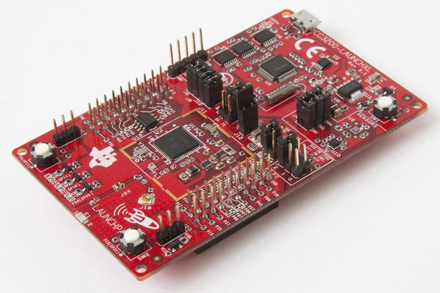
Z64-CC3200KITA
May 06, 2014Evaluation board
Equipment Class
DTS - Digital Transmission System