Z64EM4F6147RF9Development Tool
Texas Instruments Incorporated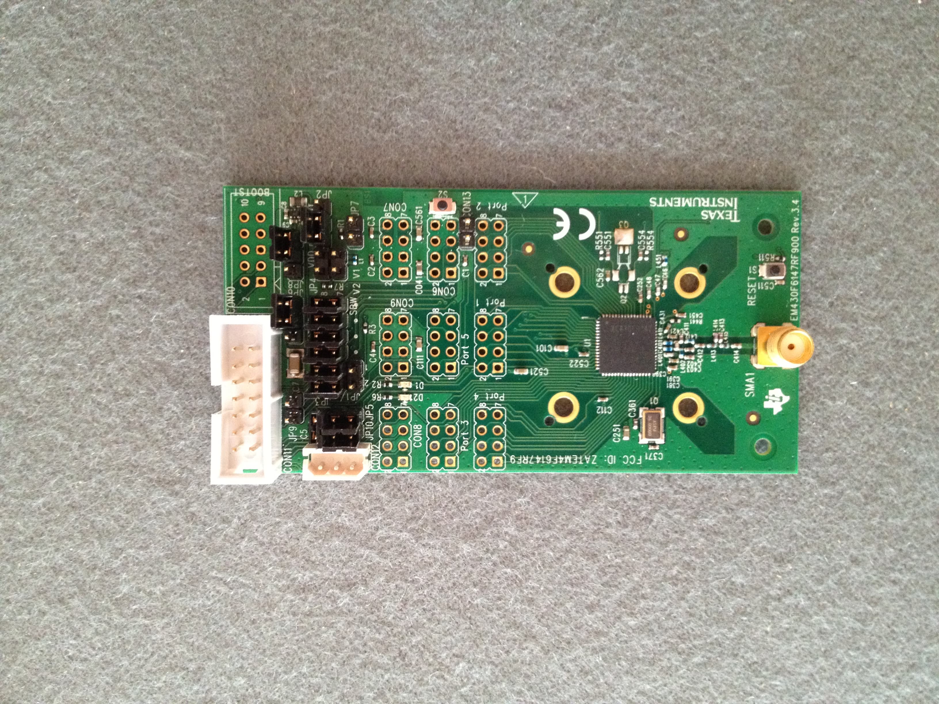
Click to zoom
Application Details
- Equipment Class
- DXT - Part 15 Low Power Transceiver, Rx Verified
- Date of Grant
- Jul 03, 2012
- Application Purpose
- Original Equipment
- Date of Application
- Jul 03, 2012
- Equipment Note
- Development Tool
- Frequency Range
- 903.49000000 - 926.49000000
- Country
- United States
Documents & Files
Document Text
Text extracted from the exhibit documents filed with the FCC. Open a document above to read the original.
Users Manual
EVALUATION BOARD/KIT/MODULE (EVM) ADDITIONAL TERMS Texas Instruments (TI) provides the enclosed Evaluation Board/Kit/Module (EVM) under the following conditions: The user assumes all responsibility and liability for proper and safe handling of the goods. Further, the user indemnifies TI from all claims arising from the handling or use of the goods. Should this evaluation board/kit not meet the specifications indicated in the User’s Guide, the board/ kit may be returned within 30 days from the date of delivery for a full refund. THE FOREGOING LIMITED WARRANTY IS THE EXCLUSIVE WARRANTY MADE BY SELLER TO BUYER AND IS IN LIEU OF ALL OTHER WARRANTIES, EXPRESSED, IMPLIED, OR STATUTORY, INCLUDING ANY WARRANTY OF MERCHANTABILITY OR FITNESS FOR ANY PARTICULAR PURPOSE. EXCEPT TO THE EXTENT OF THE INDEMNITY SET FORTH ABOVE, NEITHER PARTY SHALL BE LIABLE TO THE OTHER FOR ANY INDIRECT, SPECIAL, INCIDENTAL, OR CONSEQUENTIAL DAMAGES. Please read the User's Guide and, specifically, the Warnings and Restrictions notice in the User's Guide prior to handling the product. This notice contains important safety information about temperatures and voltages. For additional information on TI's environmental and/or safety programs, please visit www.ti.com/esh or contact TI. No license is granted under any patent right or other intellectual property right of TI covering or relating to any machine, process, or combination in which such TI products or services might be or are used. TI currently deals with a variety of customers for products, and therefore our arrangement with the user is not exclusive. TI assumes no liability for applications assistance, customer product design, software performance, or infringement of patents or services described herein. Mailing Address: Texas Instruments Post Office Box 655303 Dallas, Texas 75265 Copyright 2011, Texas Instruments Incorporated REGULATORY COMPLIANCE INFORMATION As noted in the EVM User’s Guide and/or EVM itself, this EVM and/or accompanying hardware may or may not be subject to the Federal Communications Commission (FCC) and Industry Canada (IC) rules. For EVMs not subject to the above rules, this evaluation board/kit/module is intended for use for ENGINEERING DEVELOPMENT, DEMONSTRATION OR EVALUATION PURPOSES ONLY and is not considered by TI to be a finished end product fit for general consumer use. It generates, uses, and can radiate radio frequency energy and has not been tested for compliance with the limits of computing devices pursuant to part 15 of FCC or ICES-003 rules, which are designed to provide reasonable protection against radio frequency interference. Operation of the equipment may cause interference with radio communications, in which case the user at his own expense will be required to take whatever measures may be required to correct this interference. General Statement for EVMs including a radio User Power/Frequency Use Obligations: This radio is intended for development/professional use only in legally allocated frequency and power limits. Any use of radio frequencies and/or power availability of this EVM and its development application(s) must comply with local laws governing radio spectrum allocation and power limits for this evaluation module. It is the user’s sole responsibility to only operate this radio in legally acceptable frequency space and within legally mandated power limitations. Any exceptions to this is strictly prohibited and unauthorized by Texas Instruments unless user has obtained appropriate experimental/development licenses from local regulatory authorities, which is responsibility of user including its acceptable authorization. For EVMs annotated as FCC – FEDERAL COMMUNICATIONS COMMISSION Part 15 Compliant Caution This device complies with part 15 of the FCC Rules. Operation is subject to the following two conditions: (1) This device may not cause harmful interference, and (2) this device must accept any interference received, including interference that may cause undesired operation. Changes or modifications not expressly approved by the party responsible for compliance could void the user's authority to operate the equipment. FCC Interference Statement for Class A EVM devices This equipment has been tested and found to comply with the limits for a Class A digital device, pursuant to part 15 of the FCC Rules. These limits are designed to provide reasonable protection against harmful interference when the equipment is operated in a commercial environment. This equipment generates, uses, and can radiate radio frequency energy and, if not installed and used in accordance with the instruction manual, may cause harmful interference to radio communications. Operation of this equipment in a residential area is likely to cause harmful interference in which case the user will be required to correct the interference at his own expense. FCC Interference Statement for Class B EVM devices This equipment has been tested and found to comply with the limits for a Class B digital device, pursuant to part 15 of the FCC Rules. These limits are designed to provide reasonable protection against harmful interference in a residential installation. This equipment generates, uses and can radiate radio frequency energy and, if not installed and used in accordance with the instructions, may cause harmful interference to radio communications. However, there is no guarantee that interference will not occur in a particular installation. If this equipment does cause harmful interference to radio or television reception, which can be determined by turning the equipment off and on, the user is encouraged to try to correct the interference by one or more of the following measures: • Reorient or relocate the receiving antenna. • Increase the separation between the equipment and receiver. • Connect the equipment into an outlet on a circuit different from that to which the receiver is connected. • Consult the dealer or an experienced radio/TV technician for hel…
Text truncated - open the document above for the full version.
Users Manual
Version 2.00 READ ME FIRST Thank you for purchasing a Texas Instruments development tool for our MSP430 ultra-low power microcontroller. For the latest development software, example projects, quick start guides, and tutorials please visit www.ti.com/tool/<PN>. The part number <PN> of your development tool is printed on the sticker, e.g. MSP-TS430PZ100C. To preserve our environment we do not include the printed user manual. It can be downloaded from our webpage: www.ti.com/lit/slau278 For technical support please visit the TI Engineer to Engineer community e2e.ti.com or go to www.ti.com/support Best Regards, The MSP430 Team
Users Manual
MSP430HardwareTools User's Guide LiteratureNumber:SLAU278I May2009– RevisedMay2012 Contents Preface.......................................................................................................................................7 1GetStartedNow!...............................................................................................................11 1.1FlashEmulationTool(FET)Overview..................................................................................12 1.2KitContents,MSP-FET430PIF..........................................................................................13 1.3KitContents,eZ430-F2013..............................................................................................13 1.4KitContents,eZ430-T2012..............................................................................................13 1.5KitContents,eZ430-RF2500............................................................................................13 1.6KitContents,eZ430-RF2500T...........................................................................................13 1.7KitContents,eZ430-RF2500-SEH......................................................................................13 1.8KitContents,eZ430-Chronos-xxx.......................................................................................14 1.9KitContents,MSP-FET430UIF..........................................................................................14 1.10KitContents,MSP-FET430xx............................................................................................15 1.11KitContents,FET430F6137RF900.....................................................................................16 1.12KitContents,Sub-1GHzRFSpectrumAnalyzerTool(MSP-SA430-SUB1GHZ)................................17 1.13KitContents,MSP-TS430xx.............................................................................................17 1.14KitContents,EM430Fx1x7RF900.......................................................................................19 1.15HardwareInstallation,MSP-FET430PIF...............................................................................19 1.16HardwareInstallation,MSP-FET430UIF...............................................................................19 1.17HardwareInstallation,eZ430-XXXX,MSP-EXP430G2,MSP-EXP430FR5739,MSP-EXP430F5529.........20 1.18HardwareInstallation,MSP-FET430Uxx,MSP-TS430xxx,FET430F6137RF900,EM430Fx137RF900......20 1.19ImportantMSP430DocumentsontheWeb...........................................................................20 2DesignConsiderationsforIn-CircuitProgramming...............................................................21 2.1SignalConnectionsforIn-SystemProgrammingandDebugging...................................................22 2.2ExternalPower.............................................................................................................26 2.3BootstrapLoader(BSL)..................................................................................................26 AFrequentlyAskedQuestionsandKnownIssues...................................................................27 A.1HardwareFAQs............................................................................................................28 A.2KnownIssues..............................................................................................................30 BHardware..........................................................................................................................31 B.1MSP-TS430D8.............................................................................................................33 B.2MSP-TS430PW14.........................................................................................................36 B.3MSP-TS430L092..........................................................................................................39 B.4MSP-TS430L092ActiveCable..........................................................................................42 B.5MSP-TS430PW24.........................................................................................................45 B.6MSP-TS430DW28.........................................................................................................48 B.7MSP-TS430PW28.........................................................................................................51 B.8MSP-TS430PW28A.......................................................................................................54 B.9MSP-TS430DA38..........................................................................................................57 B.10MSP-TS430QFN23x0.....................................................................................................60 B.11MSP-TS430RSB40........................................................................................................63 B.12MSP-TS430RHA40A......................................................................................................66 B.13MSP-TS430DL48..........................................................................................................69 B.14MSP-TS430RGZ48B......................................................................................................72 B.15MSP-TS430PM64.........................................................................................................75 2 ContentsSLAU278I– May2009– RevisedMay2012 SubmitDocumentationFeedback Copyright© 2009–2012,TexasInstrumentsIncorporated www.ti.com B.16MSP-TS430PM64A.......................................................................................................78 B.17MSP-TS430RGC64B.....................................................................................................81 B.18MSP-TS430RGC64C.....................................................................................................84 B.19MSP-TS430RGC64USB............................................................…
Text truncated - open the document above for the full version.
Users Manual
www.ti.comMSP-TS430RGC64B B.17MSP-TS430RGC64B FigureB-33.MSP-TS430RGC64BTargetSocketModule,Schematic 81 SLAU278I– May2009– RevisedMay2012Hardware SubmitDocumentationFeedback Copyright© 2009–2012,TexasInstrumentsIncorporated Jumper JP2 Open to disconnect LED Connector J5 External power connector Jumper JP3 to "ext" Jumpers JP5 to JP10 Close 1-2 to debug in Spy-Bi-Wire mode Close 2-3 to debug in 4-wire JTAG mode D1 LED connected to P1.0 If the system should be supplied via LDOI (J6), close JP4 and set JP3 to external Orient Pin 1 of MSP430 device MSP-TS430RGC64Bwww.ti.com FigureB-34.MSP-TS430RGC64BTargetSocketModule,PCB 82 HardwareSLAU278I– May2009– RevisedMay2012 SubmitDocumentationFeedback Copyright© 2009–2012,TexasInstrumentsIncorporated www.ti.comMSP-TS430RGC64B TableB-18.MSP-TS430RGC64BBillofMaterials No.per Pos.RefDesDescriptionDigiKeyPartNo.Comment Board 1C1,C2012pF,SMD0805DNP 2C3,C4047pF,SMD0805DNP 3C6,C7,C10310uF/6.3V,SMD0805 C5,C11, 4C13,C14,5100nF,SMD0805311-1245-2-ND C15 5C812.2nF,SMD0805 6C91470nF,SMD0805478-1403-2-ND 7C1614.7uF,SMD0805 8C171220nF,SMD0805 9D11greenLED,SMD0805P516TR-ND SAM1029-16-NDDNP:Headersandreceptacles J1,J2,J3, 10016-pinheader,TH(Header)SAM1213-16-enclosedwithkit.Keepviasfreeof J4 ND(Receptacle)solder: 11J5, J623-pinheader,male,TH JP3,JP5, placejumpersonpins2-3onJP5,JP6, JP6,JP7, 1273-pinheader,male,THSAM1035-03-NDJP7,JP8,JP9,JP10placejumperson JP8,JP9, pins1-2onJP3, JP10 JP1,JP2, 1332-pinheader,male,THSAM1035-02-NDPlacejumperonheader JP4 1410Jumper15-38-1024-NDSeePos.12andPos.13 14-pinconnector,male, 15JTAG1HRP14H-ND TH 10-pinconnector,male, 16BOOTST0"DNPKeepviasfreeofsolder" TH MicroCrystalMS3V-T1R 17Q10Crystal32.768kHz,C(Load)=DNP:Q1Keepviasfreeofsolder 12.5pF Q2:4MHzBuerklin: 18Q20CrystalDNP:Q2Keepviasfreeofsolder 78D134 http://www.ettinger.de/Art Insulating 190InsulatingdisktoQ2_Detail.cfm?ART_ARTNU disktoQ2 M=70.08.121 20R3,R72330Ω, SMD0805541-330ATR-ND R1,R2,R4, R6,R8, 2130 Ohm,SMD0805541-000ATR-NDDNP:R6,R8,R9,R10,R11,R12 R9,R10, R11,R12 22R5147kΩ, SMD0805541-47000ATR-ND Socket:QFN11T064-006- 23U11Manuf.:Yamaichi N-HSP 24PCB185x 76mm2 layers forexample,3M Adhesiveabout6mmwidth,2mm 254BumponsPartNo.SJ-Applytocornersatbottomside plasticfeetheight 5302 26D3,D4 27MSP4302MSP430F5310RGCDNP:enclosedwithkit,suppliedbyTI 83 SLAU278I– May2009– RevisedMay2012Hardware SubmitDocumentationFeedback Copyright© 2009–2012,TexasInstrumentsIncorporated 1.1 MSP-TS430RGC64C TI Friesing Tools MSP430 1 1 12/14/10 S.G. 6 5 4 3 2 1 ABCD ABCD Design: Appr.:Rev.: Comment:Drawing#: Revision: Page: File: Size: Title of Schematic of Mentor Pads Logic V9 Date: Name: 6 5 4 3 2 1 MSP-TS430RGC64C.sch <-- SBW <-- JTAG extintVCC DVIO Power Circle BSL 1 P6.0/CB0/A0 2 P6.1/CB1/A1 3 P6.2/CB2/A2 4 P6.3/CB3/A3 5 P6.4/CB4/A4 6 P6.5/CB5/A5 7 P6.6/CB6/A6 8 P6.7/CB7/A7 9 P5.0/A8/VEREF+ 10 P5.1/A9/VEREF- 11 AVCC 12 P5.4/XIN 13 P5.5/XOUT 14 AVSS 15 DVCC 16 DVSS 17 VCORE 18 P1.0/TA0CLK/ACLK 19 P1.1/TA0.0 20 P1.2/TA0.1 21 P1.3/TA0.2 22 P1.4/TA0.3 23 P1.5/TA0.4 24 P1.6/TA1CLK/CBOUT 25 P1.7/TA1.0 26 P2.0/TA1.1 27 P2.1/TA1.2 28 P2.2/TA2CLK/SMCLK 29 P2.3/TA2.0 30 P2.4/TA2.1 31 P2.5/TA2.2 32 P2.6/RTCCLK/DMAE0 33 P2.7/UCB0STE/UCA0CLK 34 P3.0/UCB0SIMO/UCB0SDA 35 P3.1/UCB0SOMI/UCB0SCL 36 P3.2/UCB0CLK/UCA0STE 37 P3.3/UCA0TXD/UCA0SIMO 38 P3.4/UCA0RXD/UCA0SOMI 39 DVSS 40 DVIO 41 P4.0/PM_UCB1STE 42 P4.1/PM_UCB1SIMO 43 P4.2/PM_UCB1SOMI 44 P4.3/PM_UCB1CLK 45 P4.4/PM_UCA1TXD 46 P4.5/PM_UCA1RXD 47 P4.6/PM_NONE 48 P4.7/PM_NONE 49 P7.0/TB0.0 50 P7.1/TB0.1 51 P7.2/TB0.2 52 P7.3/TB0.3 53 P7.4/TB0.4 54 P7.5/TB0.5 55 BSLEN 56 RST/NMI 57 P5.2/XT2IN 58 P5.3/XT2OUT 59 TEST/SBWTCK 60 PJ.0/TDO 61 PJ.1/TDI/TCLK 62 PJ.2/TMS 63 PJ.3/TCK 64 RSTDVCC/SBWTDIO 65 THERMAL_1 66 THERMAL_2 67 THERMAL_3 68 THERMAL_4 69 THERMAL_5 70 THERMAL_6 71 THERMAL_7 72 THERMAL_8 U1 MSP430F5229 1 2 3 4 5 6 7 8 9 10 11 12 13 14 JTAG 1 2 3 4 5 6 7 8 9 10 BOOTST CN-ML10 12345678910111213141516 J1 1 2 3 4 5 6 7 8 9 10 11 12 13 14 15 16 J2 123456789 10111213141516 J3 1 2 3 4 5 6 7 8 9 10 11 12 13 14 15 16 J4 123 JP5 PINHEAD_1X3 123 JP6 PINHEAD_1X3 123 JP7 PINHEAD_1X3 123 JP8 PINHEAD_1X3 123 JP9 PINHEAD_1X3 123 JP10 PINHEAD_1X3 123 J5 PINHEAD_1X3 R7 330R 123 JP3 C10 10uF C14 100nF C5 10uF C6 100nF R1 0R R2 0R R6 0R R8 0R C1 12pF C2 12pF C7 10uF C13 100nF 1 2 JP2 R3 330R 1 2 D1 ??? R4 0R C9 470nF R5 47K C8 2.2nF R11 0R R12 0R C16 4.7uF C3 tbd C4 tbd R9 0R R10 0R C15 100nF 123 J6 PINHEAD_1X3 12 JP4 PINHEAD_1X2 D3 Q2 QUARZ_4PIN 26MHz/ASX53 Q1 12 JP1 PINHEAD_1X2 SHC1 SHORTCUT2 GND GND GND GND XTLGND VCORE GND GND DVCC DVCC GND XTLGND2 GND GND DVCC GND RST/NMI TCK TMS TDI TDO RSTDVCC_SBWTDIO TDO RST/NMI TCK C TCK M TMS I TDI O TDO DVCC P1.2/TA0.1P1.1/TA0.0 TEST/SBWTCK C M I O DVCC P1.1/TA0.0 P1.2/TA0.1 RSTDVCC_SBWTDIO TEST/SBWTCK AVSS MSP-TS430RGC64Cwww.ti.com B.18MSP-TS430RGC64C FigureB-35.MSP-TS430RGC64CTargetSocketModule,Schematic 84 HardwareSLAU278I– May2009– RevisedMay2012 SubmitDocumentationFeedback Copyright© 2009–2012,TexasInstrumentsIncorporated Connector J5 External power connector for DVCC. Jumper JP3 to "ext“. IMPORTANT NOTE: Rev1.0 of the board doesn’t has connection from pin 4 of BOOST to pin 64 of MCU. In order to use BSL these pin should be connected by a wire. Jumper JP2 Open to disconnect LED D1 LED connected to P1.0 Orient Pin 1 of MSP430 device Jumpers JP5 to JP10 Close 1-2 to debug in Spy -Bi-Wire mode Close 2-3 to debug in 4-wire JTAG mode Connector J6 External power connector to supply DVIO Jumper JP4 Close if only one power supply over J5 is used for VCC and DVI www.ti.comMSP-TS430RGC64C FigureB-36.MSP-TS430RGC64CTargetSocketModule,PCB 85 SLAU278I– May2009– RevisedMay2012Hardware SubmitDocumentationFeedback Copyright© 2009–2012,TexasInstrumentsIncorporated MSP-TS430RGC64Cwww.ti.com TableB-19.MSP-TS430RGC64CBillofMaterials ItemQtyReferenceValueDescriptionCommentSupplierNo. 10C1,C212pFCAP,SMD,Ceramic,0805DNPC1C2 20C3,C4tbdCAP,SMD,Ceramic,0805DNPC3C4 43C5,C7,C1010uFCAP,SMD,Ceramic,0805 55C8C6C13-15100nFCAP,SMD,Ceramic,0805DigiKey:311-1245-…
Text truncated - open the document above for the full version.
Block Diagram
EM430F6147RF900 CC430F6147 SoC Matching Antenna MCU 26MHz XTAL Power Supply
ID Label/Location Info
Description of label for the Texas Instruments EM430F6147RF900: - Relevant imprints on PCB (Silkscreen) o Product Number/name: bottom right (“EM430F6147RF900”) o Vendor: right side “Texas Instruments” o FCC ID: left side “FCC ID: Z64EM4F6147RF9” Approx. 43 mm Figure 1: Enlarged image with imprint Figure 2: Full Board
Operational Description
PRODUCT PREVIEW ECCN5E002TSPA- Technology/ SoftwarePubliclyAvailable CC430F614x CC430F514x,CC430F512x www.ti.comSLAS555– MAY2012 MSP430SoCWithRFCore 1 FEATURES 23 •TrueSystem-on-Chip(SoC)forLow-Power –EmbeddedEmulationModule(EEM) WirelessCommunicationApplications •High-PerformanceSub-1-GHzRFTransceiver •WideSupplyVoltageRange:1.8V to3.6VCore •UltralowPowerConsumption:–SameasinCC1101 –CPUActiveMode(AM):160μA/MHz–WideSupplyVoltageRange:2.0V to3.6V –StandbyMode(LPM3RTCMode):2.0μA–FrequencyBands:300MHzto348MHz, 389MHzto464MHz,and779MHzto –OffMode(LPM4RAMRetention):1.0μA 928MHz –RTC-onlyMode(LPM3.5):1.0μA –ProgrammableDataRateFrom0.6kBaud –ShutdownMode(LPM4.5):0.3μA to500kBaud –RadioinRX:15mA,250kbps,915MHz –HighSensitivity(–117dBmat0.6kBaud,- •MSP430™SystemandPeripherals 111dBmat1.2kBaud,315MHz,1%Packet –16-BitRISCArchitecture,Extended ErrorRate) Memory,upto20-MHzSystemClock –ExcellentReceiverSelectivityandBlocking –Wake-UpFromStandbyModeinLess Performance Than6 μs –ProgrammableOutputPowerUpto+12 –FlexiblePowerManagementSystemWith dBmforAllSupportedFrequencies SVSandBrownout –2-FSK,2-GFSK,andMSKSupportedaswell –UnifiedClockSystemWithFLL asOOKandFlexibleASKShaping –16-BitTimerTA0,Timer_AWithFive –FlexibleSupportforPacket-Oriented Capture/CompareRegisters Systems:On-ChipSupportforSyncWord –16-BitTimerTA1,Timer_AWithThreeDetection,AddressCheck,FlexiblePacket Capture/CompareRegistersLength,andAutomaticCRCHandling –HardwareReal-TimeClock–SupportforAutomaticClearChannel Assessment(CCA)BeforeTransmitting(for –TwoUniversalSerialCommunication Listen-Before-TalkSystems) Interfaces –DigitalRSSIOutput –USCI_A0SupportsUART,IrDA,SPI –SuitedforSystemsTargetingCompliance –USCI_B0SupportsI 2 C,SPI WithEN300220(Europe)and –10-BitA/DConverterWithInternal FCCCFRPart15(US) Reference,Sample-and-Hold,andAutoscan –SuitedforSystemsTargetingCompliance Features(OnlyCC430F614xand WithWirelessM-BusStandardEN13757- CC430F514x) 4:2005 –Comparator –SupportforAsynchronousand –IntegratedLCDDriverWithContrast SynchronousSerialReceive/TransmitMode Controlforupto96Segments(Only forBackwardCompatibilityWithExisting CC430F614x) RadioCommunicationProtocols –128-bitAESSecurityEncryption/Decryption •FamilyMembersareSummarizedinTable1. Coprocessor •ForCompleteModuleDescriptions,Seethe –32-BitHardwareMultiplier CC430FamilyUser'sGuide(SLAU259). –Three-ChannelInternalDMA –SerialOnboardProgramming,NoExternal ProgrammingVoltageNeeded 1 Pleasebeawarethatanimportantnoticeconcerningavailability,standardwarranty,andusein criticalapplicationsof TexasInstrumentssemiconductorproductsanddisclaimerstheretoappearsattheendofthisdatasheet. 2MSP430is a trademarkofTexasInstruments. 3I 2 C is a trademarkofothers. PRODUCTPREVIEWinformationconcernsproductsinthe Copyright© 2012,TexasInstrumentsIncorporated formativeordesignphaseofdevelopment.Characteristicdataand otherspecificationsaredesigngoals.TexasInstrumentsreserves therighttochangeordiscontinuetheseproductswithoutnotice. PRODUCT PREVIEW ECCN5E002TSPA- Technology/ SoftwarePubliclyAvailable CC430F614x CC430F514x,CC430F512x SLAS555– MAY2012www.ti.com DESCRIPTION TheTexasInstrumentsCC430familyofultralow-powermicrocontrollersystem-on-chipwithintegratedRF transceivercoresconsistsofseveraldevicesfeaturingdifferentsetsofperipheralstargetedfora widerangeof applications.Thearchitecture,combinedwithsevenlow-powermodes(includingLPM3.5andLMP4.5)is optimizedtoachieveextendedbatterylifeinportablemeasurementapplications.Thedevicefeaturesthe powerfulMSP430™16-bitRISCCPU,16-bitregisters,andconstantgeneratorsthatcontributetomaximumcode efficiency. TheCC430familyprovidesa tightintegrationbetweenthemicrocontrollercore,itsperipherals,software,andthe RFtransceiver,makingthesetruesystem-on-chipsolutionseasytouseaswellasimprovingperformance. TheCC430F614xseriesaremicrocontrollersystem-on-chipconfigurationscombiningtheexcellentperformance ofthestate-of-the-artCC1101sub-1-GHzRFtransceiverwiththeMSP430CPUXV2,upto32kBofin-system programmableflashmemory,upto4 kBofRAM,two16-bittimers,a high-performance10-bitA/Dconverterwith eightexternalinputsplusinternaltemperatureandbatterysensors,comparator,universalserialcommunication interfaces(USCI),128-bitAESsecurityaccelerator,hardwaremultiplier,DMA,real-timeclockmodulewithalarm capabilities,LCDdriver,andupto44I/Opins. TheCC430F514xandCC430F512xseriesaremicrocontrollersystem-on-chipconfigurationscombiningthe excellentperformanceofthestate-of-the-artCC1101sub-1-GHzRFtransceiverwiththeMSP430CPUXV2,up to32kBofin-systemprogrammableflashmemory,upto4 kBofRAM,two16-bittimers,a highperformance10- bitA/DconverterwithsixexternalinputsplusinternaltemperatureandbatterysensorsonCC430F514xdevices, comparator,universalserialcommunicationinterfaces(USCI),128-bitAESsecurityaccelerator,hardware multiplier,DMA,real-timeclockmodulewithalarmcapabilities,andupto30I/Opins. Typicalapplicationsforthesedevicesincludewirelessanaloganddigitalsensorsystems,heatcostallocators, thermostats,metering(AMR/AMI),smartgridwirelessnetworksetc. Familymembersavailablearesummarizedin Table1. Forcompletemoduledescriptions,seetheCC430FamilyUser's Guide(SLAU259). Table1.FamilyMembers USCI ChannelChannel ProgramSRAMTimer_AADC10_APackage DeviceLCD_B (2) Comp_BI/O A:B: (KB)(KB) (1)(2) Type UART/LINSPI/I 2 C /IrDA/SPI 8 ext/ CC430F61473245,396seg118 ch.4464RGC 4 intch. 8 ext/ CC430F61451625,396seg118 ch.4464RGC 4 intch. 8 ext/ CC430F6143825,396seg118 ch.4464RGC 4 intch. 6 ext/ CC430F51473245,3n/a116 ch.3048RGZ 4 intch. 6 ext/ CC430F51451625,3n/a116 ch.3048RGZ 4 intch. 6 ext/ CC430F5143825,3n/a116 ch.3048RGZ 4 intch. CC430F51251625,3n/a11n/a6 ch.3048RGZ CC430F5123825,3n/a11n/a6 ch.3048RGZ (1)Eachnumberin thesequencerepresentsaninstantiationofTimer_AwithitsassociatednumberofcapturecompareregistersandPWM outputgeneratorsavailable.Forexample,a numbersequenceof5,3 wouldrepresenttwoinstantiationsofTimer_A,thefirst instantiationhaving5 andthesecondinstantiationhaving3 capturecompareregistersandPWMoutputgenerators,respectively. (2)n/a:notavaila…
Text truncated - open the document above for the full version.
Operational Description
Technical description for Texas Instruments EM430F6147RF900: The EM430F6147RF900 is an evaluation board for the CC430F6147 chip from Texas Instruments. The board will only fully function once software has been downloaded to the CC430F6147 System on Chip (SoC). This may be done with the Texas Instruments MSP-FET430UIF or MSP-FET430PIF JTAG interface, which is required to program or control the device. Per default, the EM430F6147RF900 is pre-programmed with a blinking LED software, the does neither receive nor transmit RF signals. User software needs to be generated and downloaded onto the CC430F6147 SoC in order use the board beyond the blinking LED function. The CC430F6147 System on Chip has a differential RF output. On the EM430F6147RF900 board this differential output is transformed to a single ended, 50 ohm signal through a passive component (capacitor/inductor) balun. The output of the balun is filtered to reduce harmonic radiation and then connected to an SMA connector. The antenna supplied with the board is S463AM-915 from Nearson. The datasheet of the antenna is attached for further details. Frequency range: 902 – 928MHz (North America) Type of modulation: 2-GFSK Occupied bandwidth: 11.2kHz Antenna connector: standard SMA This evaluation board is intended for use for ENGINEERING DEVELOPMENT, DEMONSTRATION OR EVALUATION PURPOSES ONLY and is not considered by TI to be a finished end product fit for general consumer use.
Parts List/Tune Up Info
Part List Report for EM430F6147RF900 Date: 20/01/2011 Initial Version from CAD Rev4.025.04.2012 MPTools BOM Rev3.320.01.2011 THInitial Version from CAD 20.01.2011 THJumperplan ergänzt 27.01.2011 THU2,L2,C8,C9 vorerst DNP 23.03.2011 THmod, added Pos 6 7 31 47 48 Rev3.4 and Rev3.4S11.07.2011 THcopied from V3.3, JP9 added, BOM prepared for PCB Rev 3.4(U1 direct) and 3.4S(U1 with Socket) 19.10.2011 THPCB Name changed to EM430F6147RF900 Rev4.020.4.2012 THonly Layoutchange , no part depending Notes: 1. These assemblies are ESD sensitive, ESD precautions shall be observed. 2. These assemblies must comply with workmanship standards IPC-A-610 Class 2. 3. All values with DNP means this Part is not mounted 4. Ref designators marked with RED cannot be substituted. All other components can be substituted with equivalent MFG's components. 5. Capacitors w/o detailed MFGR and Supplier could have 20% and >= 16V 6. Resistors w/o detailed MFGR and Supplier could have 5%. ItemQtyReferenceValueDescriptionMFGRMFGR#MFGR-FootprintSupplierSupplier#Provided by 12ABO1-2BohrungBohrungLayout--Layout-DNP 21APCB1 PCB EM430F6147RF900 Rev4 Tools PCB Coordinate Lower/Left-----DNP 33AVB1-3Fiducial Mark Bottom-SeiteFiducial MarkLayout--Layout-DNP 4 3AVT1-3Fiducial Mark Top-SeiteFiducial MarkLayout--Layout-DNP 514C1-5 C112 C252 C381 C391 C421 C431 C451 C522 C5620.1uFCAP, SMD, Ceramic, 0402, 0.1uF, 16V, 10%, X5RAVX0402YC104KAT2A402tbdtbd 61C722uFCapacitor, Ceramic, 1206, 16V, X5R, 20%SanyoGRM31CR61C226ME15L1206tbdtbd 72C8-92.2uFCAP, SMD, Ceramic, 0402, 2.2uF, X5RMurataGRM155R60J225ME15D402tbdtbd 81C0414.7uFCAP, SMD, Ceramic, 0603, 4.7uF, 16V, 10%, X5Rtbdtbd603tbdtbd 94C46-47 C392 C482pFCAP, SMD, Ceramic, 0402, 2pF, 50V, +/-0.1pF, COGMurataGRM1555C1H2R0BZ01402tbdtbd 101C1010.47uFCAPACITOR,SMT,0603,CERAMIC,0.47uF,16V,10%,X5RAVX0603YD474KAT2A603tbdtbd 114C111 C251 C521 C5611uFCAPACITOR,SMT,0603,CERAMIC,1uF,6.3V,10%,X5RPANASONICECJ-1VB0J105K603tbdtbd 122C361 C37127pFCAP, SMD, Ceramic, 0402, 27pF, 50V, 5%, COG(NPO)MurataGRM36COG270J50402tbdtbd 131C4011pFCAPACITOR,SMT,0402,CER,1pF,50V,+/-0.25pF,NP0MurataGJM1555C1H1R0CB01D402tbdtbd 144C402 C411-412 C4141.5pFCAPACITOR,SMT,0402,CERAMIC,1.5pF,50V,+/-0.25pF,C0G(NP0)MurataGRM1555C1H1R5CZ01402tbdtbd 151C403100pFCAPACITOR,SMT,0402,CERAMIC,100pF,50V,+/-5%,C0G(NP0)MurataGRM1555C1H101JZ01402tbdtbd 161C4138.2pFCAPACITOR,SMT,0402,CERAMIC,8.2pF,50V,+/-0.25pF,C0G(NP0)MurataGRM1555C1H8R2CZ01402tbdtbd 171C5112.2nFCAPACITOR,SMT,0402,CER,2200pF,50V,10%,X7RPANASONICECJ-0EB1H222K402tbdtbd 182C554 C55112pFCAPACITOR,SMT,0402,CER,12pF,50V,5%,NPOPANASONICECJ-0EC1H120J402tbdtbdDNP 199CON1-92x4Pin,Rm.2.54(DNP)Header, THD, Male 2x4 Pin, 100mil spacingtbdtbd2x4Pin,Rm.2.54tbdtbdDNP, but put in box 201CON102x5Pin,Wanne(DNP)Header, THD, Male 2x5 Pin, Wanne, 100mil spacingtbdtbd2x5Pin,WannetbdtbdDNP 211CON112x7Pin,WanneHeader, THD, Male 2x7 Pin, Wanne, 100mil spacingtbdtbd2x7Pin,Wannetbdtbd 221CON12Molex1x3Pinheader 1x3, Grid: 2.5mmMolex3/22/50351x3Pin,Rm2.5mmtbdtbd 23a4JP3 JP5 JP9 JP101x2PinPinheader 1x2; Grid: 100mil / 2.54 mm 23b2CON13 JP71x2PinPinheader 1x2; Grid: 100mil / 2.54 mmDNP 241D1SMD LED LAMP(GREEN)LED,SMT,0603,GREEN,2.1VKINGBRIGHTAPT1608MGC1.6mmX0.8mm-- 251D2SMD LED LAMP(Red)LED,SMT,0603,RED,2.0VKINGBRIGHTAPT1608EC1.6mmX0.8mm-- 261JP12x4PinPinheader 2x4 Grid: 100mil / 2.54 mm 271JP1A2x3PinPinheader 2x3: Grid: 100mil / 2.54 mm 283JP2 JP6 JP81x3PinPinheader 1x3, Grid: 100mil / 2.54mm 291JP42x2PinPinheader 2x2: Grid: 100mil / 2.54 mmDNP 303L1 L401 L41112nHInductor, SMD, 0402, 12n…
Text truncated - open the document above for the full version.
Contact Information
Applicant
Marian Kost(Product Line Manager, Connectivity)
Technical Contact
Texas InstrumentsFritz R Ward
[email protected](214) 567-9484
12500 TI Boulevard, M/S 8669 · Dallas, Texas · United States
Non-Technical Contact
Nemko USA, Inc.Zarah G. MacIvor
[email protected]214-629-5683
Test Firm
Nemko Dallas, Inc.Mike Cantwell
Technical Specifications
| # | Rule Parts | Frequency Range | Power Output |
|---|---|---|---|
| 1 | 15C | 903.49 MHz - 926.49 MHz | - |
Other Applications from Texas Instruments Incorporated
Z64-CC33SBMOD
Jul 17, 2025802.11 b/g/n/ax WLAN + BLE Radio Module
Equipment Class
DTS - Digital Transmission System
Z64-CC3200MODR1
Oct 08, 2014Radio Module
Equipment Class
DTS - Digital Transmission System
Z64-CC3100MODR1
Oct 08, 2014Radio Module
Equipment Class
DTS - Digital Transmission System
Z64-CC3100KITA
May 06, 2014Evaluation board
Equipment Class
DTS - Digital Transmission System
Z64-CC3200KITA
May 06, 2014Evaluation board
Equipment Class
DTS - Digital Transmission System