ZAT110190EM915The CC1101-CC1190EM-915 is a development tool for TIs sub-1 GHz CC1101 and CC1190 devices.
Texas Instruments Inc.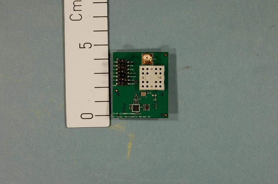
Click to zoom
Application Details
- Equipment Class
- DTS - Digital Transmission System
- Date of Grant
- Dec 01, 2013
- Application Purpose
- Original Equipment
- Date of Application
- Dec 01, 2013
- Equipment Note
- The CC1101-CC1190EM-915 is a development tool for TIs sub-1 GHz CC1101 and CC1190 devices.
- Frequency Range
- 903.50000000 - 926.50000000
- Company
- Texas Instruments Inc.
- Country
- United States
Documents & Files
Document Text
Text extracted from the exhibit documents filed with the FCC. Open a document above to read the original.
Users Manual
SWRU284A November 2013 CC1101-CC1190EMK Quick Start Guide Opening the box and using the modules with SmartRF04EB 1. Kit Contents 2 x CC1101-CC1190EM (869 or 915 MHz) 2 x Pulse W5017 Antennas (2 dBi) The 869 MHz RF board is tested to comply with ETSI/R&TTE over temperatures from 0 to +70°C. The 915 MHz RF board is FCC and IC certified. The boards should not be modified to operate in other frequency bands than what they have been designed for. FCC/IC Regulatory Compliance (915 MHz board only) FCC Part 15 Class A Compliant IC ICES-003 Class A Compliant 2. How to Use the Modules The CC1101-CC1190 Evaluation Module (EM) boards can be plugged into the SmartRF04EB (EB), which is included in the CC1101DK. This board lets you control the devices from SmartRF™ Studio and it can also be used as a development platform. The evaluation module is also supported by the SmartRF TrxEB, included in the CC11xL, CC1120 and CC1200 development kits. This Quick Start Guide describes how to properly power the SmartRF04EB with a CC1101-CC1190EM and how to control the combo from SmartRF Studio. 3. Plug EM into SmartRF04EB Insert the EM into the EB. Attach the antenna firmly. Caution! The kit contains ESD sensitive components. Handle with care to prevent permanent damage. To minimize risk of injury, avoid touching components during operation if symbolized as hot. 4a. Apply Power The EB can be powered from different sources: USB, Battery or an External Power Supply The voltage regulator on the EB supplies 3.3 V to the assembly, but it can only source up to 150 mA. It cannot supply the CC1101-CC1190EM since it can consume more than 300 mA. An external power supply is therefore required for powering the EM. It is possible to have separate power sources for the EB and for the EM. This is controlled with the strap between I_OUT and I_IN on P5 (the screw terminal). Remove it to allow separate power supplies. 4b. Power the EB Connect the EB to a USB port on a PC. Alternatively, connect a 9 V, non- rechargeable, alkaline battery (not included in the kit) to the battery connector on the bottom side of the board. Note that if multiple power sources are connected, the source with the highest voltage will power the EB. This means that you should disconnect any attached battery when using USB power; otherwise the battery will be drained. 4c. Power the EM As noted in 4a, remove the strap on P5 and connect the external power supply as shown in the picture above. The red wire is the positive supply and the black wire is GND. This will power the EM directly from the external power supply, whereas the rest of the EB will be powered from USB or the battery. The power supply range should be within 3.0 to 3.6 V. 4d. Optional: Same Power Supply for both EB and EM Connect a 3.3 V voltage source between the 3.3 V and 0 V terminals. 3.3 V is the middle terminal. In this case, the on-board voltage regulator will be bypassed. Note that the strap on P5 should not be removed. 5. Set Power Switch If EB and EM are powered from different sources as described in 4a-4c, the switch should be set to the rightmost position. If EB and EM are powered from the same external supply as described in 4d, the switch should be set to the leftmost position. This switch can be used to turn off the EB by switching it to the opposite position of that used to turn it on. 6. External Power Supply Range With the test setup in 4a-4c, the EB is connected to a 3.3 V supply through the on-board voltage regulator and the EM is powered by the external supply. Since the EB is powered through a regulated 3.3 V supply the signals going from CC1101- CC1190 to the EB (and vice versa) need to be within 3.0 V to 3.6 V. The external supply connected to the EM when using the setup in 4a-4c is therefore limited to 3.0 V to 3.6 V. With the setup in 4d the supply range is limited 2.7 V to 3.6 V. External Power Supply 1 Requirements: Nom Voltage: 3.3VDC Max Current: 800 mA Efficiency Level V 1 When using an external power supply, make sure it meets the listed requirements in addition to complying with applicable regional product regulatory and safety certification requirements such as UL, CSA, VDE, CCC, and PSE GND VDD SWRU284A November 2013 SmartRF™ Studio 1. Download and Install SmartRF Studio Before connecting the EB to your PC, download SmartRF™ Studio from www.ti.com/smartrfstudio. Install the program and follow the instructions in the wizard. Connect the EB with a CC1101-CC1190EM to the PC using the USB cable and install the USB driver as described in the manual. 2. Launch SmartRF Studio Launch SmartRF Studio and double click on the highlighted CC1101 device icon to get complete control of the device from the PC. You can now configure the radio, run tests, export register settings and run link tests with another CC1101-CC1190EM on a SmartRF04EB connected to the PC. 3. Configure the Radio In order to control the CC1190 select CC1190 as “Range Extender” and select the appropriate “EM Revisions” as shown (either 869 or 915 MHz). You can now use all the features in Studio as for a standalone EM. Test the performance of the radio using some of these features: Continuous TX: Output power, spectrum Continuous RX: Received signal strength, synchronous/asynchronous serial RX mode Packet TX/RX: Link and sensitivity testing References Please visit http://www.ti.com/product/cc1190 http://www.ti.com/tool/cc1101cc1190emk868 http://www.ti.com/tool/cc1101cc1190emk915 http://www.ti.com/lit/swra356 (Using the CC1190 Front End with CC1101 under EN 300 220) http://www.ti.com/lit/swra361 (Using the CC1190 Front End with CC1101 under FCC 15.247) Download the SmartRF™ Studio software, as well as datasheets, reference designs and application notes. You will also find a lot of information on the TI E2E forum at http://e2e.ti.com We hope you will enjoy working with the CC1101 and CC1190 devices. EVALUATIONBOARD/KIT/MODULE(EVM)ADDITIONALTERMS TexasInstruments(TI)providestheenclosedEvaluatio…
Text truncated - open the document above for the full version.
Block Diagram
f = <902MHz – 928MHz> LNA PA FREQUENCY SYNTHESIZER f_internal = <5412MHz – 5568MHz> f_output = <902MHz – 928MHz> AAF ADCADC DEMODULATOR MODULATOR RADIO CONTROLLER AND DATA INTERFACE RF_P RF_N XOSC_Q2 XOSC_Q1 13MHz RC-OSC 34.7kHz RC-OSC 26MHz Crystal OSC IQ Q I BALUN CTRL CC1190 SAW filter
External Photos
PHOTOSof EUT Project no.:215176 FCC ID: ZAT110190EM915 Page1of3 INTERNALPHOTOS–CC1101-CC1190EM-915 CC1101-CC1190EM-915, EUT PHOTOSof EUT Project no.:215176 FCC ID: ZAT110190EM915 Page2of3 Antenna PHOTOSof EUT Project no.:215176 FCC ID: ZAT110190EM915 Page3of3 CC1101-CC1190EM-915,hosted on TrxEB TrxEB with 2xAA Batteries
ID Label/Location Info
Certification Document Label 1/1 Description of label for CC1101-CC1190EM-915 FCC/IC labeling of product is shown below. There is a separate label with the model name, optional variant designator, revision number, serial number, FCC ID and IC identifier. The placement of the label on the product is shown below. ~ 39.4 mm ~ 4 6 . 5 m m M o d e l : C C 1 1 0 1 - C C 1 1 9 0 E M - 9 1 5 ( x x ) R e v . x . x . x S . N o . : x x x x x x F C C I D : Z A T 1 1 0 1 9 0 E M 9 1 5 I C : 4 5 1 H - 1 1 0 1 9 0 E M 9 1 5 Front Side Back Side Label manufacturer is Brady. Label part number B473 (http://www.bradyid.com/bradyid/domino/contentView.do/B473.html) with print using series R6000 ribbons (R6007 - http://www.bradyid.com/bradyid/pdpv/IP-R6007.html).
Internal Photos
PHOTOSof EUT Project no.:215176 FCC ID: ZAT110190EM915 Page1of3 INTERNALPHOTOS–CC1101-CC1190EM-915 CC1101-CC1190EM-915, EUT PHOTOSof EUT Project no.:215176 FCC ID: ZAT110190EM915 Page2of3 Antenna PHOTOSof EUT Project no.:215176 FCC ID: ZAT110190EM915 Page3of3 CC1101-CC1190EM-915,hosted on TrxEB TrxEB with 2xAA Batteries
Operational Description
Texas Instruments Norway AS Gaustadalléen 21 0349 Oslo Norway (+47) 22 95 85 44 (+47) 22 95 85 46 Technical Description The CC1101-CC1190EM-915, see Figure 1, includes Texas Instruments’ CC1101, which is a sub-1 GHz transceiver designed for low power wireless applications and CC1190, which is an RF Front End for low-power and low-voltage wireless applications at 850 - 950 MHz. CC1101 has a balanced output (RF_N and RF_P), which is transformed to a single ended signal through a passive component (capacitor/inductor) balun. The output of the balun is filtered by a SAW filter and then connected to CC1190. The output of the CC1190 is connected to an SMA connector. The CC1190 is enclosed by a standard surface mount RF shield. The antenna supplied with the board is W5012 from Pulse Electronics. The antenna datasheet is attached for further details. The CC1101-CC1190EM-915 cannot be pre-programmed and neither CC1101 nor CC1190 will in active mode (transmit or receive) at power-up. The user needs to configure CC1101 and CC1190 into active mode. Figure 1 CC1101-CC1190EM-915
Parts List/Tune Up Info
Ref. Part name Pcs/unit Description Manufacture r Part numbe r U1 CC1101 1 Single-chip transceiver TI CC1101 U2 CC1190 1 LNA and PA 26 dBm TI CC1190 C28 C_0402 1 Capacitor, general, 0402; Do not mount C125 C_0P8_0402_NP0_B_50 1 Capacitor, 0.8p, 0402, NP0, +/-0.1pF, 50V Murata GRM1555C1HR80BZ01D C41;C51;C91;C111;C141;C151;C181 C_100N_0402_X5R_K_10 7 Capacitor, 100n, 0402, X5R, 10%, 10V Murata GRM155R71A104KA01D C124 C_100P_0402_NP0_J_50 1 Capacitor, 100p, 0402, NP0, 5% 50V Murata GRM1555C1H101JZ01D C2 C_10U_0603_X5R_M_4 1 Capacitor, 10u, 0603, X5R, 20%, 4V Murata GRM188R60G106ME47D C22;C52;C81 C_12P_0402_NP0_J_50 3 Capacitor, 12p, 0402, NP0, 5%, 50V Murata GRM1555C1H120JZ01D C101;C132 C_15P_0402_NP0_J_50 2 Capacitor, 15p, 0402, NP0, 5%, 50V Murata GRM1555C1H150JZ01D C27 C_1N_0402_NP0_J_50 1 Capacitor, 1n, 0402, NP0, 5%, 50V Murata GRM1555C1H102JA01D C121 C_1P0_0402_NP0_C_50 1 Capacitor, 1p, 0402, NP0, +/-0.25pF 50V Murata GRM1555C1H1R0CZ01D C122;C131 C_1P5_0402_NP0_C_50 2 Capacitor, 1p5, 0402, NP0, +-0.25pF, 50V Murata GRM1555C1H1R5CZ01D C1;C30 C_1U_0402_X5R_K_6P3 2 Capacitor, 1u, 0402, X5R, 10%, 6.3V Murata GRM155R60J105KE19D C3 C_220P_0402_NP0_J_50 1 Capacitor, 220p, 0402, NP0, 5%, 50V Murata GRM1555C1H221JA01D C161 C_27P_0402_NP0_J_50 1 Capacitor, 27p, 0402, NP0, 5%, 50V Murata GRM1555C1H270JZ01D C24 C_3P3_0402_NP0_C_50 1 Capacitor, 3p3, 0402, NP0, +-0.25pF, 50V Murata GRM1555C1H3R3CZ01D C21;C26;C123 C_47P_0402_NP0_J_50 3 Capacitor, 47p, 0402, NP0, 5%, 50V Murata GRM1555C1H470JZ01D C25 C_7P5_0402_NP0_C_50 1 Capacitor, 7p5, 0402, NP0, +/-0.25pF 50V Murata GRM1555C1H7R5CZ01D U3 EPCOS_B3588 1 SAW filter, 915 MHz EPCOS B3588 L25 L_10N_0402_G_LQW 1 Inductor, 10n, 0402, ±2%, wire-wound type Murata LQW15AN10NG00D L2 L_11N_0402_J_LQW 1 Inductor, 11n, 0402, ±5%, wire-wound type Murata LQW15AN11NJ00 L121;L131 L_12N_0402_J_LQW 2 Inductor, 12n, 0402, ±5%, wire-wound type Murata LQW15AN12NJ00D L122;L132 L_18N_0402_J_LQW 2 Inductor, 18n, 0402, ±5%, wire-wound type Murata LQW15AN18NJ00D L130 L_1N5_0402_S 1 Inductor, 1n5, 0402, Monolithic type, +/-0.3 nH Murata LQG15HS1N5S02D L21 L_22N_0603_J_LQW 1 Inductor, 22n, 0603, ±5%, wire-wound type Murata LQW18AN22NJ10 L23 L_2N9_0402_B_LQW 1 Inductor, 2n9, 0402, wire-wound type, ±0.1nH Murata LQW15AN2N9B00D L22 L_7N5_0402_G_LQW 1 Inductor, 7n5, 0402, ±2%, wire-wound type Murata LQW15AN7N5G00 L24 L_9N1_0402_G_LQW 1 Inductor, 9n1, 0402, ±2%, wire-wound type Murata LQW15AN9N1G00D L1 L_BEAD_102_0402 1 EMI filter bead, 0402 1k ohms Tape GHz Band Gen Use Murata BLM15HG102SN1D P4 PINROW_SMD_2X7_2.54MM_ P 1 2x7 pinrow, 2.54mm pitch, SMD type with locating peg GradConn BB02-HP141-KB3-060A00 R3-5 R_10K_0402_F 3 Resistor, 10k ohms, 0402, ±1% Koa RK73H1ETTP1002F R161 R_10_0402_G 1 Resistor, 10 ohms, 0402, 2% Koa RK73H1ETTP10R0F (±1%) R141 R_3K3_0402_F 1 Resistor, 3k3 ohms, 0402, ±1% Koa RK73H1ETTP3301F R151 R_47_0402_G 1 Resistor, 47 ohms, 0402, 2% Koa RK73H1ETTP47R0F (±1%) R171 R_56K_0402_F 1 Resistor, 56k ohms, 0402, ±1% Koa RK73H1ETTP5602F P3 SMA_SMD 1 SMA connector, straight SMD-mount Hus-Tsan Group Taiwan SMA-10V21-TGG P1-2 SMD_SOCKET_2x10 2 SMD pinrow socket, .050 spacing, 2x10 Samtec SFM-110-02-SM-D-A-K-TR P5 Shield BMIS-202 1 Surface Mount Shield Two-Piece. Cover ordered separately Laird BMI-S-202-F P5 cover Shield BMIS-202 cover 1 Cover for SHIELD BMIS-202 Laird BMI-S-202-C X1 X_26.000/20/40/40/10 1 Crystal, 26.000000MHz, 10.0pF, 50 ohms max, 20/40 ppm, -40C t NDK NX3225GA, EXS00A-CG01
RF Exposure Info
Prediction of MPE limit at a given distance Equation from page 18 of OET Bulletin 65, Edition 97-01 where:S = power density P = power input to the antenna G = power gain of the antenna in the direction of interest relative to an isotropic radiator R = distance to the center of radiation of the antenna Maximum peak output power at antenna input terminal:13.0(dBm)* Maximum peak output power at antenna input terminal:20.0(mW) Antenna gain(maximum):4.4(dBi)* Maximum antenna gain:2.75(numeric) Time Averaging:100(%)* Prediction distance:20(cm)* Prediction frequency:925(MHz)* MPE limit for uncontrolled exposure at prediction frequency:0.617(mW/cm^2) Power density at prediction frequency:0.011(mW/cm^2) This equates to:0.11W/m^2 2 4R PG S π =
RF Exposure Info
SAR Exclusion Justification for FCC ID ZAT110190EM915 Test exclusion thresholds for 100 MHz to 6 GHz at test separation distances ≤ 50 mm Guidance document reference: 447498 D01 General RF Exposure Guidance v05r01, page 11, paragraph 4.3.1(1). The 1-g and 10-g SAR test exclusion thresholds for 100 MHz to 6 GHz at test separation distances ≤ 50 mm are determined by: [(max. power of channel, including tune-up tolerance, mW)/(min. test separation distance, mm)] * [√f(GHz)] ≤ 3.0 for 1-g SAR and ≤ 7.5 for 10-g extremity SAR, where • f(GHz) is the RF channel transmit frequency in GHz • Power and distance are rounded to the nearest mW and mm before calculation • The result is rounded to one decimal place for comparison • 3.0 and 7.5 are referred to as the numeric thresholds in the step 2 below The test exclusions are applicable only when the minimum test separation distance is ≤ 50 mm and for transmission frequencies between 100 MHz and 6 GHz. When the minimum test separation distance is < 5 mm, a distance of 5 mm according to 5) in section 4.1 is applied to determine SAR test exclusion. SAR test exclusion analysis: Assumptions: Since the exact separation distance may vary from sensor to sensor, the minimum separation distance of 5 mm is assumed per the guidance document. Max. power of channel:20 mW Min. separation distance:5 mm Max. frequency: 0.925GHz [(Pwr/Dist)*Freq.] =3.70 The result of the above SAR threshold calculation demonstrates that the result is less than the 10-g numeric threshold of 7.5. Conclusion: The above analysis shows that the digital transmission system transceiver with FCC ID ZAT110190EM915 qualifies for exemption from SAR testing. Signed: Tom Tidwell, Technical Manager 21 October, 2013 Nemko USA, Inc.
Test Report
Nemko AS, Gaustadalléen 30, P.O.Box 73 Blindern, NO-0314 Oslo Norway T +47 22 96 03 30 F +47 22 96 05 50 Enterprise number NO974404532 Visiting address: Nemko Kjeller, Instituttveien 6, P.O.Box 96, NO-2027 Kjeller Norway T +47 64 84 57 00 F +47 64 84 57 05 Test report no. : 215176-1 Item tested : CC1101-CC1190EM-915 Type of equipment : 902 - 928MHz Transceiver FCC ID : ZAT110190EM915 Client : Texas Instruments Norway AS FCC Part 15.247 Digital Transmission System RSS-210, Issue 8 Low Power Licence-Exempt Radiocommunication Devices 15 November 2013 Authorized by : .............................................. Frode Sveinsen Technical Verificator TEST REPORT FCC part 15.247 Ref. no.: 215176-1 FCC ID: ZAT110190EM915 IC: 451H-110190EM915 Nemko AS, NO-2027 Kjeller Page 2 (42) CONTENTS 1 GENERAL INFORMATION ...................................................................................................... 3 1.1 Testhouse Info .......................................................................................................................... 3 1.2 Client Information ...................................................................................................................... 3 1.3 Responsible Manufacturer (If other than client) ........................................................................ 3 2 TEST INFORMATION ............................................................................................................... 4 2.1 Test Item ................................................................................................................................... 4 2.2 Test Environment ...................................................................................................................... 5 2.3 Test Period................................................................................................................................ 5 3 TEST REPORT SUMMARY ..................................................................................................... 6 3.1 General ..................................................................................................................................... 6 3.2 Test Summary ........................................................................................................................... 7 3.3 Description of modification for Modification Filing ..................................................................... 7 3.4 Comments ................................................................................................................................ 7 3.5 Family List Rational .................................................................................................................. 7 4 TEST RESULTS ....................................................................................................................... 8 4.1 Minimum 6 dB Bandwidth ......................................................................................................... 8 4.2 20 dB Bandwidth ..................................................................................................................... 12 4.3 Peak Power Output ................................................................................................................. 14 4.4 Spurious Emissions ................................................................................................................ 24 4.5 Power Spectral Density (PSD) ................................................................................................ 37 5 LIST OF TEST EQUIPMENT .................................................................................................. 41 6 BLOCK DIAGRAM ................................................................................................................. 42 6.1 Power Line Conducted Emission ............................................................................................ 42 6.2 Test Site Radiated Emission ................................................................................................... 42 TEST REPORT FCC part 15.247 Ref. no.: 215176-1 FCC ID: ZAT110190EM915 IC: 451H-110190EM915 Nemko AS, NO-2027 Kjeller Page 3 (42) 1 GENERAL INFORMATION 1.1 Testhouse Info Name : Nemko AS Address : Nemko Kjeller Instituttveien 6, Box 96 NO-2027 Kjeller, NORWAY Telephone : +47 64 84 57 00 Fax : +47 64 84 57 05 E-mail: [email protected] FCC test firm : 994405 IC OATS : 2040D-1 Total Number of Pages: 42 1.2 Client Information Name : Texas Instruments Norway AS Address : Gaustadalléen 21, NO-0349 Oslo, Norway Telephone : +47 22 95 85 44 Fax : +47 22 95 85 46 Contact: Name : Dag Grini Telephone : +47 22 95 83 01 E-mail : [email protected] 1.3 Responsible Manufacturer (If other than client) Same as the client. TEST REPORT FCC part 15.247 Ref. no.: 215176-1 FCC ID: ZAT110190EM915 IC: 451H-110190EM915 Nemko AS, NO-2027 Kjeller Page 4 (42) 2 TEST INFORMATION 2.1 Test Item Name : Texas Instruments FCC ID : ZAT110190EM915 IC : 451H-110190EM915 Model/version : CC1101-CC1190EM-915 Serial number : - Hardware identity and/or version: - Software identity and/or version : - Frequency Range : 903.5 – 926.5 MHz Number of Channels : - Type of Modulation : Digital (4-FSK) Conducted Output Power: 20 mW (Peak) User Frequency Adjustment : None Type of Power Supply : 3.0V DC (Two AA 1.5 V DC batteries) Antenna Connector : SMA, Antenna type Pulse W5017 Antenna Diversity Supported : No Desktop Charger : None Description of Test Item The CC1101-CC1190EM-915 is a RF-transceiver module with receiver and a range extender. TEST REPORT FCC part 15.247 Ref. no.: 215176-1 FCC ID: ZAT110190EM915 IC: 451H-110190EM915 Nemko AS, NO-2027 Kjeller Page 5 (42) 2.2 Test Environment 2.2.1 Normal test condition Temperature: 21.6 – 22.2 °C Relative humidity: 41.7 – 42.7 % Normal test voltage: Nominal 3.0 V DC (2 x AA battery ) New batteries were used for all tests. The values are the limit registered during the test period. 2.3 Test Per…
Text truncated - open the document above for the full version.
Test Setup Photos
Photos of TestSet-up Project no.:215176 FCC ID:ZAT110190EM915 Page1of2 PHOTOS OF TEST SET-UP–CC1101-CC1190EM-915 XY plane-Radiated Emissions Radiated emissions-< 30MHz, 10meter Photos of TestSet-up Project no.:215176 FCC ID:ZAT110190EM915 Page2of2 RadiatedEmissions30-902 & 902-1000MHz, 3 meter Radiated emissions 1–10GHz, 3 meter
Contact Information
Applicant
Marian Kost(Product Line Manager, Connectivity)
Test Firm
Nemko ASFrode Sveinsen
Technical Specifications
| # | Rule Parts | Frequency Range | Power Output |
|---|---|---|---|
| 1 | 15C | 903.5 MHz - 926.5 MHz | 20.00 mW |
Other Applications from Texas Instruments Inc.
ZAT-2340R5MODA
Jan 30, 2026CC2340R5MODAN0MHAR
Equipment Class
DTS - Digital Transmission SystemZAT-1312PSIP-3
May 19, 2024CC1312PSIP
Equipment Class
DSS - Part 15 Spread Spectrum TransmitterZAT-1312PSIP-2
Jan 21, 2024CC1312PSIP
Equipment Class
DSS - Part 15 Spread Spectrum Transmitter
ZAT-1312PSIP-1
Jul 09, 2023CC1312PSIP
Equipment Class
DSS - Part 15 Spread Spectrum Transmitter
ZAT7IDEM
Feb 27, 2014The 7IDEM is a development tool for TIs 2.4 GHz 7ID System-on-Chip
Equipment Class
DTS - Digital Transmission System