ZAT1120EM900The CC1120EM-868-915 is a development tool for the sub-1 GHz CC1120 RF transceiver chip from Texas Instruments.
Texas Instruments Inc.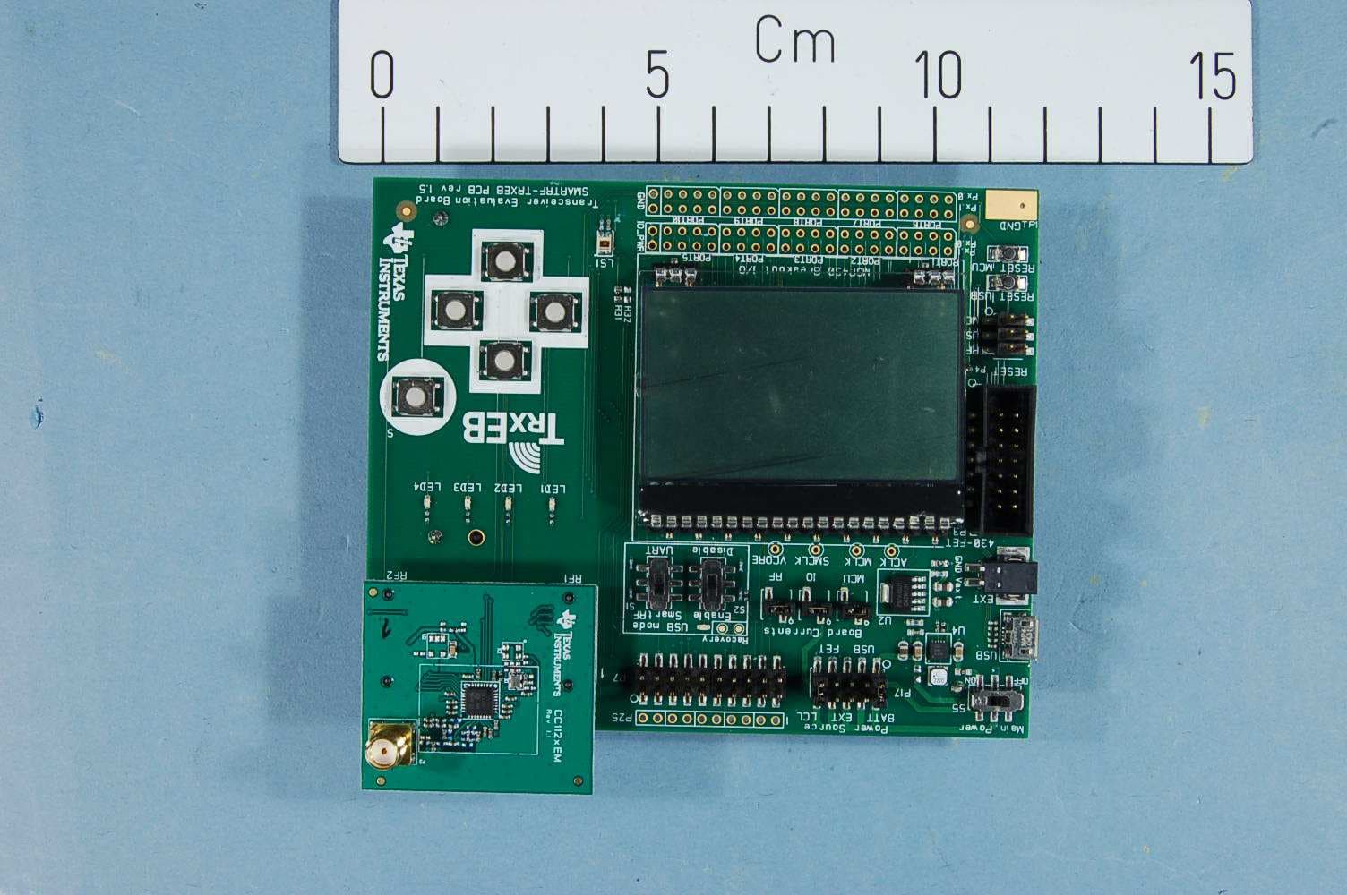
Click to zoom
Application Details
- Equipment Class
- DXT - Part 15 Low Power Transceiver, Rx Verified
- Date of Grant
- Apr 22, 2013
- Application Purpose
- Original Equipment
- Date of Application
- Apr 22, 2013
- Equipment Note
- The CC1120EM-868-915 is a development tool for the sub-1 GHz CC1120 RF transceiver chip from Texas Instruments.
- Frequency Range
- 903.50000000 - 926.50000000
- Company
- Texas Instruments Inc.
- Country
- United States
Documents & Files
Document Text
Text extracted from the exhibit documents filed with the FCC. Open a document above to read the original.
Users Manual
SWRU291B November 2012 Web sites: www.ti.com/lprf E2E Forum: www.ti.com/lprf-forum Make sure to subscribe to the Low-Power RF Newsletter to receive information about updates to documentation, new product releases, and more. Sign up on the TI web pages. CC112x Evaluation Module Kit Quick Start Guide Opening the Box and Running the Packet Error Rate Test 1. Kit Contents 2 x CC1120 or CC1121 Evaluation Modules 2 x Antennas (type depending on frequency) The EMK is an add-on kit to supplement the CC1120DK with evaluation boards supporting additional frequency bands. This document covers the CC1120EMK and CC1121EMK. Antenna types: 955 & 868-915 MHz: Pulse W5017 420-470 MHz: Pulse SPWH24433TI 169 MHz: Pulse SPHL24169TI 2. How to use the Modules The CC112xEM boards can be plugged into several development boards from Texas Instruments. Most notably, you can use the SmartRF Transceiver EB, which is included in the CC1120DK. This board lets you run a packet error rate (PER) test, control the device from SmartRF™ Studio and it can be used as a development platform. It is also possible to connect the EM to other TI development boards with the appropriate connectors or to the basic “SoC Battery Board”. The latter can be used as a carrier board for the EM to simplify the connection to other boards with a microcontroller. See: http://www.ti.com/tool/soc-bb This guide will show how to use the modules together with SmartRF Transceiver EB (TrxEB). 3. Plug the EM into the TrxEB Insert a CC112xEM into the TrxEB. Do not use excessive force on the EM. Remember to mount the antenna. Caution! The kit contains ESD sensitive components. Handle with care to prevent permanent damage. To minimize risk of injury, avoid touching components during operation if symbolized as hot. The hardware in this kit is tested and complies with ETSI/R&TTE over temperature from 0 to +35°C. The W5017 whip antenna from Pulse has a gain of 2 dBi 4. Select Board Mode Use the switches S1 and S2 to select the operating mode of the board. For the sake of this quick start guide, please select “Enable” and “UART”. This configuration will make it possible to communicate directly with the MSP430 over a virtual COM port on the PC. 5. Power Options There are several ways of applying power to the TrxEB. 2 x 1.5 V AA batteries USB External Power Supply MSP430 Debugger For the batteries and USB, there are voltage regulators on the TrxEB that will set the on-board voltage to 3.3 V. Warning! To minimize risk of injury or property damage, never use rechargeable batteries to power the board. Always select a power source that is suitably rated for use with this EVM, not exceeding 3.6 VDC, with a current output rating between 0 and 500 mA. 6. Select Power Source Depending on the power source, make sure you connect jumpers to the appropriate pins on the “Power Source” header. For instance, if you use batteries, use a jumper to short-circuit pin 1 and 2 on the header. See back side of board for explanation of the jumpers. Note that there should only be one active power source at any one time. Do not leave the EVM powered when unattended. 7. Welcome Screen Turn on power with the Main Power switch. You should now see the Texas Instruments logo and a short description of the buttons on the LCD. Pushing any of the five buttons on the board will take you to the main menu. NB! If you don’t see anything on the screen make sure the mode switches are in the correct positions (see step 4 above). 8. Packet Error Rate Test Select the PER (Packet Error Rate) test by highlighting the selection using the up/down buttons. Confirm your selection by pressing Enter (right button). 9. Select Test Mode The PER test can be run is several modes. Easy Mode sets up a one-way test and uses default settings. This test is convenient for practical range testing. The other test modes are described in the “Software Examples for CC112x, CC11xL and CC1101 User’s Guide”. To proceed, highlight “Easy Mode” and press Enter (right button). 10. Select Frequency Select which frequency to use for the test. Make sure that the evaluation modules you have match the selected frequency. 11. Select Mode One of the boards must operate as the slave (transmitter) and the other as master (receiver). Select Slave on one board... ...and Master on the other board. 12. Establish Link The slave node will now wait for a configuration package from the Master. The configuration contains the parameters used for the PER test. The configuration package will be sent when you select “link devices” on the master node. 13. Link Established When the initial linking has completed, the slave node will start the test by continuously transmitting packets to the master. 14. Start the Receiver (master) On the master node, you can select the number of packets you want to receive in order to calculate the packet error. When selecting “Start PER Test”, the master (receiver) will begin to count the number of received packets and provide some statistics. 15. PER Test Results The master will display a window that plots the received signal strength (RSSI) for each packet. Press the “Up” button to go to the detailed statistical window. 16. PER Test Results The statistics window will show the error rate based on the number of lost or erroneous packets divided by the total number of packets that should have been received. 17. Troubleshooting It you are experiencing problems with this test, please check the following: Nothing is shown in the display! Unfortunately, the first series of TrxEB uses a connector that doesn’t fit exactly to the pins of the LCD. It should be sufficient to tilt the LCD slightly to get a snug fit with the connector. Please visit the kit web page and check for updated SW and documentation. Updated SW can be downloaded to the device using IAR EW430 or SmartRF Flash Programmer. If you get poor PER results at short distances, try to move the transmitter and receiver further apart. The CC1120/CC1121 receive…
Text truncated - open the document above for the full version.
Block Diagram
CC1120EM-868-915 CC1120 f = <902MHz – 928MHz> LNA PA FREQUENCY SYNTHESIZER f_internal = <3608MHz – 3712MHz> f_output = <902MHz – 928MHz> AAF ADC ADC DEMODULATOR MODULATOR RADIO CONTROLLER AND DATA INTERFACE LNA_N LNA_P CLOCK MUX X O S C _ Q 2 X O S C _ Q 1 32678kHz RC-OSC 32MHz Crystal OSC IQ Q I CTRL Balun Passive LC network PA
External Photos
FCC ID: ZAT1120EM900 & IC ID: 451H-1120EM900 Project no.: 215168 Page 1 of 2 EXTERNAL PHOTOS – CC1120EM-868-915 CC1120EM-868-915 with the W5017 antenna FCC ID: ZAT1120EM900 & IC ID: 451H-1120EM900 Project no.: 215168 Page 2 of 2 CC1120EM-868-915 hosted on TrxEB TrxEB with 2xAA Batteries
ID Label/Location Info
Certification Document Label 1/1 Description of label for CC1120EM-868-915 FCC/IC/CE labeling of product is shown below. There is a separate label with the model name, optional variant designator, revision, serial number, FCC ID and IC number. Texas Instruments Model: CC1120EM-868-915 (xx) Rev. x.x.x S.No.: xxxxxx FCC ID: ZAT1120EM900 IC: 451H-1120EM900 ~ 1 3 m m ~ 25 mm Placement of label on product ~39 mm ~ 3 6 m m T e x a s I n s t r u m e n t s M o d e l : C C 1 1 2 0 E M - 8 6 8 - 9 1 5 ( x x ) R e v . x . x . x S . N o . : x x x x x x F C C I D : Z A T 1 1 2 0 E M 9 0 0 I C : 4 5 1 H - 1 1 2 0 E M 9 0 0 Front side Back side Label manufacturer is Brady. Label part number B473 (http://www.bradyid.com/bradyid/domino/contentView.do/B473.html) with print using series R6000 ribbons (R6007 - http://www.bradyid.com/bradyid/pdpv/IP-R6007.html).
Internal Photos
FCC ID: ZAT1120EM900 & IC ID: 451H-1120EM900 Project no.: 215168 Page 1 of 2 EXTERNAL PHOTOS – CC1120EM-868-915 CC1120EM-868-915 with the W5017 antenna FCC ID: ZAT1120EM900 & IC ID: 451H-1120EM900 Project no.: 215168 Page 2 of 2 CC1120EM-868-915 hosted on TrxEB TrxEB with 2xAA Batteries
Operational Description
Texas Instruments Norway AS Gaustadalléen 21 0349 Oslo Norway (+47) 22 95 85 44 (+47) 22 95 85 46 Technical Description The CC1120EM-868-915 is an evaluation board for the CC1120 RF transceiver chip from Texas Instruments. The board will only function together with the SmartRF Transceiver Evaluation Board (TrxEB) which is included in the CC1120 Development Kit. The CC1120 has a single ended PA output and a differential LNA input. On the CC1120EM-868-915 board these RF inputs and outputs are combined and transformed to a 50 ohm signal through a passive component (capacitor/inductor) balun. The output of the balun is low pass filtered to reduce harmonic radiation and then connected to an SMA connector. The CC1120EM-868-915 board is equipped with an 868 - 928 MHz whip antenna W5017 from Pulse. The antenna gain is 2 dBi.
Parts List/Tune Up Info
CC112x EM Rev 1.1.0 868_915 MHz version Including LPF Ref. Part namePcs/unitDescriptionManufacturerPart number C11 C_47N_0402_X7R_K_251Capacitor, 47n, 0402, X7R, 10%, 25VMurataGRM155R71E473KA88D C12 C_100N_0402_X5R_K_100Do not mount C41 C_10N_0402_X7R_K_250Do not mount C51 C_47N_0402_X7R_K_251Capacitor, 47n, 0402, X7R, 10%, 25VMurataGRM155R71E473KA88D C52 C_2U2_0603_X5R_K_101Capacitor, 2u2, 0603, X5R, 10%, 10VMurataGRM188R61A225KE34D C53C_04020Do not mount C61 C_220N_0402_X5R_K_101Capacitor, 220n, 0402, X5R, 10%, 10VMurataGRM155R61A224KE19D C121C_47N_0402_X7R_K_251Capacitor, 47n, 0402, X7R, 10%, 25VMurataGRM155R71E473KA88D C131C_47N_0402_X7R_K_251Capacitor, 47n, 0402, X7R, 10%, 25VMurataGRM155R71E473KA88D C151C_47N_0402_X7R_K_251Capacitor, 47n, 0402, X7R, 10%, 25VMurataGRM155R71E473KA88D C171C_10N_0402_X7R_K_251Capacitor, 10n, 0402, X7R, 10%, 25VMurataGRM155R71E103KA01D C172C_100P_0402_NP0_J_501Capacitor, 100p, 0402, NP0, 5% 50VMurataGRM1555C1H101JZ01D C173C_33P_0402_NP0_J_501Capacitor, 33p, 0402, NP0, 5%, 50VMurataGRM1555C1H330JZ01D C174C_15P_0402_NP0_J_501Capacitor, 15p, 0402, NP0, 5%, 50VMurataGRM1555C1H150JA01D C175C_3P0_0402_NP0_C_501Capacitor, 3p0, 0402, NP0, +-0.25pF, 50VMurataGRM1555C1H3R0CZ01D C176C_1P0_0402_NP0_B_501Capacitor, 1p, 0402, NP0, +/-0.1pF 50VMurataGRM1555C1H1R0BZ01D C177C_04020Do not mount C181C_2P2_0402_NP0_C_501Capacitor, 2p2, 0402, NP0, +-0.25pF, 50VMurataGRM1555C1H2R2CZ01 C191C_3P3_0402_NP0_C_501Capacitor, 3p3, 0402, NP0, +-0.25pF, 50VMurataGRM1555C1H3R3CZ01D C201C_3P3_0402_NP0_C_501Capacitor, 3p3, 0402, NP0, +-0.25pF, 50VMurataGRM1555C1H3R3CZ01D C211C_10N_0402_X7R_K_251Capacitor, 10n, 0402, X7R, 10%, 25VMurataGRM155R71E103KA01D C221C_47N_0402_X7R_K_251Capacitor, 47n, 0402, X7R, 10%, 25VMurataGRM155R71E473KA88D C231C_1N8_0402_U2J_J_101Capacitor, 1n8, 0402, U2J, 5%, 10VMurataGRM1557U1A182JA01D C251C_47N_0402_X7R_K_251Capacitor, 47n, 0402, X7R, 10%, 25VMurataGRM155R71E473KA88D C261 C_47N_0402_X7R_K_251Capacitor, 47n, 0402, X7R, 10%, 25VMurataGRM155R71E473KA88D C271 C_47N_0402_X7R_K_251Capacitor, 47n, 0402, X7R, 10%, 25VMurataGRM155R71E473KA88D C281 C_47N_0402_X7R_K_251Capacitor, 47n, 0402, X7R, 10%, 25VMurataGRM155R71E473KA88D C291 C_47N_0402_X7R_K_251Capacitor, 47n, 0402, X7R, 10%, 25VMurataGRM155R71E473KA88D C301 C_15P_0402_NP0_J_501Capacitor, 15p, 0402, NP0, 5%, 50VMurataGRM1555C1H150JA01D C302 C_04020Do not mount C311 C_15P_0402_NP0_J_501Capacitor, 15p, 0402, NP0, 5%, 50VMurataGRM1555C1H150JA01D C321 C_100N_0402_X5R_K_100Do not mount C322 C_22P_0402_NP0_J_500Do not mount L1 L_BEAD_102_04021EMI filter bead, 0402 1k ohms Tape GHz Band Gen UseMurataBLM15HG102SN1D L171 L_10N_0402_J_LQW1Inductor, 10n, 0402, ±5%, wire-wound typeMurataLQW15AN10NJ00D L172 L_7N5_0402_G_LQW1Inductor, 7n5, 0402, ±2%, wire-wound typeMurataLQW15AN7N5G00 L173 L_18N_0402_J_LQW1Inductor, 18n, 0402, ±5%, wire-wound typeMurataLQW15AN18NJ00D L174 L_12N_0402_J_LQW1Inductor, 12n, 0402, ±5%, wire-wound typeMurataLQW15AN12NJ00D L191 L_15N_0402_J_LQW1Inductor, 15n, 0402, ±5%, wire-wound typeMurataLQW15AN15NJ00D L192 L_12N_0402_J_LQW1Inductor, 12n, 0402, ±5%, wire-wound typeMurataLQW15AN12NJ00D L193 L_12N_0402_J_LQW1Inductor, 12n, 0402, ±5%, wire-wound typeMurataLQW15AN12NJ00D L201 L_12N_0402_J_LQW1Inductor, 12n, 0402, ±5%, wire-wound typeMurataLQW15AN12NJ00D P1 SMD_SOCKET_2x101SMD pinrow socket, .050 spacing, 2x10SamtecSFM-110-02-SM-D-A-K-TR P2 SMD_SOCKET_2x101SMD pinrow socket, .050 spacing, 2x10SamtecSFM-110-02-SM-D-A-K-TR P3 SMA_SMD1SMA connector, straight SMD-mount R12 R_0_04021Resistor, 0 ohm, 0402KoaRK73Z1ETTP R141 R_56K_0402_F1Resistor, 56k ohms, 0402, ±1% KoaRK73H1ETTP5602F R171 R_10_0402_J1Resistor, 10 ohms, 0402, 5%KoaRK73H1ETTP10R0F (±1%) R321 R_04020Do not mount R322 R_0_04020Do not mount U1 CC11201TI tranciverTexas Instruments U2 TPS799300Do not mount X1 X_32.000/10/20/60/101Crystal, 32.000000MHz, FA-128, 10.0pF, +/-10ppm, (FTC: +/-20ppm at -40/85C), 60ohms Epson ToyocomFA-128, 32MHZ, 10PPM, 10PF, 2x1.6mm, -40/+85C, 60ohms X2 TG_5021CG0Do not mount 43
Schematics
VDD_REG VDD_REG 3V3A VDD_REG VDD_REG 3V3A VDD_REG VDD_REG VDD_REG VDD_REG VDD_REG VDD_REG VDD_REG 1 2 C302C_0402 1 2 C41 C_10N_0402_X7R_K_25 1 2 C131 C_47N_0402_X7R_K_25 1 2 C173C_33P_0402_NP0_J_50 1 23 4 N.C.Vcc OUT GND TCXO X2 TG_5021CG 1 2 C221 C_47N_0402_X7R_K_25 1 2 C211 C_10N_0402_X7R_K_25 12 L1 L_BEAD_102_0402 1 2 L171 L_10N_0402_J_LQW 1 2 C301 C_15P_0402_NP0_J_50 1 2 C231 C_1N8_0402_U2J_J_10 1 2 34 56 78 910 1112 1314 1516 1718 1920 GPIO0 GPIO2 SCLK P1 SMD_SOCKET_2X10 1 2 C261 C_47N_0402_X7R_K_25 1 2 C12 C_100N_0402_X5R_K_10 1 2 C121 C_47N_0402_X7R_K_25 1 2 C11 C_47N_0402_X7R_K_25 1 2 C177 C_0402 1 2 R322R_0_0402 1 2 C171 C_10N_0402_X7R_K_25 1 2 C311 C_15P_0402_NP0_J_50 1 2 3 4 5 OUT IN NR EN GND U2 TPS79930 12 L172 L_7N5_0402_G_LQW 1 2 C52 C_2U2_0603_X5R_K_10 1 2 C61 C_220N_0402_X5R_K_10 12 R12 R_0402 12 L173 L_18N_0402_J_LQW 12 C191 C_3P3_0402_NP0_C_50 1 2 C172 C_100P_0402_NP0_J_50 1 2 C51 C_47N_0402_X7R_K_25 1 2 C322 C_22P_0402_NP0_J_50 1 2 C321 C_100N_0402_X5R_K_10 1 2 L192 L_12N_0402_J_LQW 1 2 C281 C_47N_0402_X7R_K_25 1 2 C271 C_47N_0402_X7R_K_25 1 2 C291 C_47N_0402_X7R_K_25 1 2 C251 C_47N_0402_X7R_K_25 1 2 R141 R_56K_0402_F 1 2 C151 C_47N_0402_X7R_K_25 1 2 R321 R_0402 12 34 56 78 910 1112 1314 1516 1718 1920 P2 SMD_SOCKET_2X10 1 2 C53 C_0402 1 2 3 4 5 6 7 8 910111213141516 17 18 19 20 21 22 23 24 25 2627282930313233 RESET GPIO3 MOSI MISO CSN EP EXT_XOSC AVDD_SYNTH DCPL_XOSC AVDD_GUARD DCPL_PFD_CHP CS_N LNA_N LNA_P DVDD LFC_0 RESET_N AVDD_IF PA DVDD NC SI RBIAS DCPL_VCO AVDD_XOSC AVDD_FRONTEND DCPL_DREG XOSC_Q1 XOSC_Q2 SCLK AVDD_SYNTH_CMOS AVDD_PFD_CHP TRX LFC_1 GPIO3 GPIO2 SO/GPIO1GPIO0 U1 CC112X 12 C174 C_15P_0402_NP0_J_50 1 2 L191 L_15N_0402_J_LQW 1 2 L193 L_12N_0402_J_LQW 1 2 3 4 5 P3 SMA_SMD 12 L201 L_12N_0402_J_LQW 1 2 R171 R_10_0402_J 12 L174 L_12N_0402_J_LQW 1 2 C175 C_3P0_0402_NP0_C_50 1 2 C181 C_2P2_0402_NP0_C_50 1 2 C201 C_3P3_0402_NP0_C_50 1 2 C176 C_1P0_0402_NP0_B_50 FM2 FIDUCIAL_MARK FM1 FIDUCIAL_MARK FM3 FIDUCIAL_MARK 1 2 3 4 GND X1X_32.000/10/20/60/10 A3 SCALESHEET APPROVALS DATE REV.DWG NO. DWG COMPANY NAME ISSUED CHECKED DRAWN FSCM NO.SIZE CONTRACT NO. Texas Instruments C177: do not mount CC1120/25 uning XTAL: do not mount: X2, C321, C322, R321, R322 CC1120/25 using TCXO: do not mount: R12, R321, C311, X1. C301: mount 0 Ohm resisitor X1: CC1120:32MHz and CC1125:40MHz R12 is a 0ohms shunt resistor that ground the EXT_XOSC pin when TCXO is not mounted. 1 of 1 03236 868/915 MHz frequency band 1.1.0 FRS L1 is a Bead to be mounted if the regulator U2 is not mounted, CC1120 ref des will default not use regulator CC1120/CC1125: do not mount: U2, C12, C41, C53 TG5021CG is optional: do not mount L1 if regulator is mounted
Test Report
Nemko AS, Gaustadalléen 30, P.O.Box 73 Blindern, NO-0314 Oslo Norway T +47 22 96 03 30 F +47 22 96 05 50 Enterprise number NO974404532 Visiting address: Nemko Kjeller, Instituttveien 6, P.O.Box 96, NO-2027 Kjeller Norway T +47 64 84 57 00 F +47 64 84 57 05 Test report no. : 215168-4 Item tested : CC1120EM-868-915 Type of equipment : Low power transceiver module 903.5 – 926.5 MHz FCC ID : ZAT1120EM900 Client : Texas Instruments Norway AS FCC Part 15.249 Low Power Transmitter 902-928 MHz Band RSS-210, Issue 8 Low-Power Licence-exempt Radiocommunications devices 902 – 928 MHz Band 28 November 2012 Authorized by : .............................................. Frode Sveinsen Technical Verificator TEST REPORT FCC part 15.249 Project no.: 215168-4 FCC ID: ZAT1120EM900 & IC ID: 451H-1120EM900 Nemko AS, NO-2027 Kjeller Page 2 (33) CONTENTS 1 GENERAL INFORMATION ...................................................................................................... 3 1.1 Testhouse info .......................................................................................................................... 3 1.2 Client information ...................................................................................................................... 3 1.3 Manufacturer ............................................................................................................................. 3 2 TEST INFORMATION ............................................................................................................... 4 2.1 Test item ................................................................................................................................... 4 2.2 Test environment ...................................................................................................................... 5 2.3 Test period ................................................................................................................................ 5 3 TEST REPORT SUMMARY ..................................................................................................... 6 3.1 General ..................................................................................................................................... 6 3.2 Test summary ........................................................................................................................... 7 3.3 Description of modification for modification filing ...................................................................... 7 3.4 Comments ................................................................................................................................ 7 3.5 Family list rationale ................................................................................................................... 7 4 TEST RESULTS ....................................................................................................................... 8 4.1 Occupied bandwidth ................................................................................................................. 8 4.2 Peak power output .................................................................................................................. 12 4.3 Spurious Emissions (Radiated) .............................................................................................. 22 5 LIST OF TEST EQUIPMENT .................................................................................................. 31 6 BLOCK DIAGRAM ................................................................................................................. 32 6.1 System set up for radiated measurements ............................................................................. 32 6.2 Test Site Radiated Emission ................................................................................................... 33 TEST REPORT FCC part 15.249 Project no.: 215168-4 FCC ID: ZAT1120EM900 & IC ID: 451H-1120EM900 Nemko AS, NO-2027 Kjeller Page 3 (33) 1 GENERAL INFORMATION 1.1 Testhouse info Name : Nemko AS Address : Nemko Kjeller Instituttveien 6, Box 96 NO-2027 Kjeller, NORWAY Telephone : +47 64 84 57 00 Fax : +47 64 84 57 05 Email: [email protected] FCC test firm : 994405 IC OATS : 2040D-1 Total Number of Pages: 33 1.2 Client information Name : Texas Instruments Norway AS Address : Gaustadalléen 21, NO-0349 Oslo, Norway Telephone : +47 22 95 85 44 Fax : +47 22 95 85 46 Contact: Name : Dag Grini Telephone : +47 22 95 83 01 E-mail : [email protected] 1.3 Manufacturer Same as client TEST REPORT FCC part 15.249 Project no.: 215168-4 FCC ID: ZAT1120EM900 & IC ID: 451H-1120EM900 Nemko AS, NO-2027 Kjeller Page 4 (33) 2 TEST INFORMATION 2.1 Test item Name : Texas Instruments Model/version : CC1120EM-868-915 FCC ID: ZAT1120EM900 IC ID: 451H-1120EM900 Serial number : 0852 Hardware identity and/or version: 1.1.0 Software identity and/or version : - Frequency Range : 903.5 – 926.5 MHz Number of Channels : 3 Operating Modes : TX and RX Type of Modulation : 2-GFSK Data rate: 38.4kbit/s User Frequency Adjustment : None, Software controlled Conducted Output Power : 0.12 mW Type of Power Supply : Battery (tested with 2 AA batteries) Antenna Connector : SMA female Antenna type: Pulse W5017, rod antenna Antenna Diversity Supported : None Description of test item The CC1120EM-868-915 is an RF-transceiver module, which is hosted on a TrxEB motherboard during testing.. TEST REPORT FCC part 15.249 Project no.: 215168-4 FCC ID: ZAT1120EM900 & IC ID: 451H-1120EM900 Nemko AS, NO-2027 Kjeller Page 5 (33) 2.2 Test environment 2.2.1 Normal test condition Temperature: 20 – 21 °C Relative humidity: 29 – 43 % Normal test voltage: 3.3 V DC The values are the limit registered during the test period. 2.3 Test period Item received date: 2012-10-20 Test period : from 2012-10-26 -2012-11-02 TEST REPORT FCC part 15.249 Project no.: 215168-4 FCC ID: ZAT1120EM900 & IC ID: 451H-1120EM900 Nemko AS, NO-2027 Kjeller Page 6 (33) 3 TEST REPORT SUMMARY …
Text truncated - open the document above for the full version.
Test Setup Photos
FCC ID: ZAT1120EM900 & IC ID: 451H-1120EM900 Project no.: 215168 Page 1 of 2 PHOTOS OF TEST SET-UP – CC1120EM-868-915 Radiated emissions - In band – VP Radiated emissions 30 – 1000 MHz FCC ID: ZAT1120EM900 & IC ID: 451H-1120EM900 Project no.: 215168 Page 2 of 2 Radiated emissions >1 GHz Radiated emissions > 8.5 GHz
Contact Information
Applicant
Marian Kost(Product Line Manager, Connectivity)
Test Firm
Nemko ASFrode Sveinsen
Technical Specifications
| # | Rule Parts | Frequency Range | Power Output |
|---|---|---|---|
| 1 | 15C | 903.5 MHz - 926.5 MHz | - |
Other Applications from Texas Instruments Inc.
ZAT-2340R5MODA
Jan 30, 2026CC2340R5MODAN0MHAR
Equipment Class
DTS - Digital Transmission SystemZAT-1312PSIP-3
May 19, 2024CC1312PSIP
Equipment Class
DSS - Part 15 Spread Spectrum TransmitterZAT-1312PSIP-2
Jan 21, 2024CC1312PSIP
Equipment Class
DSS - Part 15 Spread Spectrum Transmitter
ZAT-1312PSIP-1
Jul 09, 2023CC1312PSIP
Equipment Class
DSS - Part 15 Spread Spectrum Transmitter
ZAT7IDEM
Feb 27, 2014The 7IDEM is a development tool for TIs 2.4 GHz 7ID System-on-Chip
Equipment Class
DTS - Digital Transmission System