ZAT2531NANOThe CC2531NANO is a miniaturized USB dongle for ZigBee� RF4CE applications.
Texas Instruments Inc.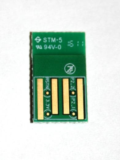
Click to zoom
Application Details
- Equipment Class
- DTS - Digital Transmission System
- Date of Grant
- Feb 02, 2012
- Application Purpose
- Original Equipment
- Date of Application
- Feb 02, 2012
- Equipment Note
- The CC2531NANO is a miniaturized USB dongle for ZigBee� RF4CE applications.
- Frequency Range
- 2405.00000000 - 2480.00000000
- Company
- Texas Instruments Inc.
- Country
- United States
Documents & Files
Document Text
Text extracted from the exhibit documents filed with the FCC. Open a document above to read the original.
Users Manual
CC2531 NANO USB stick User’s Guide 2/21 Table of Contents 1 INTRODUCTION ...................................................................................................................... 4 2 ACRONYMS AND ABBREVIATIONS ................................................................................... 5 3 HW REQUIREMENTS ............................................................................................................. 6 4 NANO USB STICK SERIAL BOOT LOADER ...................................................................... 7 4.1 SOFTWARE REQUIRED .................................................................................................................... 7 4.2 SBL BOOT CODE IMAGE ............................................................................................................... 8 4.3 DOWNLOAD THE SERIAL BOOTLOADER ....................................................................................... 8 4.4 SBL COMPATIBLE APPLICATION CODE IMAGE .............................................................................. 9 4.5 GENERATING A BINARY FILE:........................................................................................................ 9 4.5.1 Note on the batch files: ............................................................................................................................................... 13 4.5.2 Modify the code placement: ........................................................................................................................................ 13 4.6 DOWNLOAD A NEW APPLICATION IMAGE VIA SBL ..................................................................... 14 4.6.1 Serially boot the new Application Image (binary file): ................................................................................................... 14 4.6.2 Remark about the Application .................................................................................................................................... 15 4.7 COMMON ISSUES ........................................................................................................................ 15 4.7.1 SmartRF Programmer bug: ........................................................................................................................................ 15 4.7.2 USB Driver issues: ....................................................................................................................................................... 15 5 SCHEMATIC AND LAYOUT ................................................................................................ 15 6 DOCUMENT HISTORY ......................................................................................................... 15 3/21 Table of Figures Figure 1: NANO USB stick and standard USB stick .................................................................. 6 Table of Tables Table 1: NANO USB and standard USB pin assignements ....................................................... 7 4/21 1 Introduction The NANO USB stick is a miniature USB interface for 2.4GHz wireless applications. The design is based on a CC2531 System-on-Chip with an IEEE 802.15.4 radio. The NANO USB stick supports ZigBee and RF4CE applications. Typical applications includes: ZigBee RF4CE USB HID(Human Interface Device) ZigBee RF4CE serial port interface ZigBee gateway and commisioning interface for PC The NANO USB stick simplifies development of USB interface for ZigBee and RF4CE applications. The small and low cost design allows integration of ZigBee and RF4CE into PCs, Set-Top boxes, TVs, tablets and smart phones. The NANO USB stick provides an easy integration of ZigBee and RF4CE radios into all types of electronics with USB interface The since the NANO USB stick is FCC/ETSI certified you can use the product with full confidence that the product will pass certification and significantly reduce design times. For customers that want to make their own products the reference design files are available upon request. 5/21 2 Acronyms and Abbreviations LED Light Emitting Diode LPW Low Power Wireless MCU Micro Controller RF Radio Frequency RF4CE Radio Frequency for Consumer Electronic SoC System on Chip TI Texas Instruments USB Universal Serial Bus 6/21 3 HW requirements Since the NANO USB stick has no I/O connections or LEDs for user interface it is recommended to use a standard CC2531 USB dongle for SW development and prototyping before loading the code onto the NANO USB stick. The NANO USB stick is compatible with regards to USB interface and radio interface to the standard CC2531 USB dongle. Figure 1: NANO USB stick and standard USB stick The table below lists the difference in I/O pin connections between the NANO USB stick and the CC2531 USB dongle Pin name CC2531 dongle NANO USB stick P0_0 LED GND P0_1 Not connected GND P0_2 I/O Pin header GND P0_3 I/O Pin header GND P0_4 I/O Pin header GND P0_5 I/O Pin header GND P0_6 Not connected GND P0_7 Not connected GND P1_0 USB pull-up USB pull-up P1_1 LED GND P1_2 Push button GND P1_3 Push button GND P1_4 I/O Pin header GND P1_5 I/O Pin header GND 7/21 P1_6 I/O Pin header GND P1_7 I/O Pin header GND P2_0 Not connected GND P2_1 Debug data Debug data P2_2 Debug clock Debug clock P2_3 Not connected GND P2_4 Not connected GND Table 1: NANO USB and standard USB pin assignments The debug interface on the NANO USB stick is accessible on test points between the USB connector pins but these test points are small and difficult to access. Hence it is recommended to use the USB bootloader code programmed into the device for loading application code onto the device. All unused I/Os should be configured as input pull-down at the beginning of your application to reduce current consumption. 4 NANO USB Stick Serial Boot Loader This section will guide you through the steps needed to build a Serial Boot Loader (SBL) for a Z-stack and for an RF4CE application and will explain you how to modify such an ap…
Text truncated - open the document above for the full version.
Block Diagram
USB USB PHY DM DP 1 KB FIFO SRAM CC2531 MEMORY ARBITER 8051 CPU CORE DMA 32/64/128/256 KB FLASH 8 KB SRAM FLASH CTRL DEBUG INTERFACE RESET RESET_ N P2_4 P2_3 P2_2 P2_1 P2_0 P1_4 P1_3 P1_2 P1_1 P1_0 P1_7 P1_6 P1_5 P0_4 P0_3 P0_2 P0_1 P0_0 P0_7 P0_6 P0_5 32.768 kHz CRYSTAL OSC 32 MHz CRYSTAL OSC HIGH SPEED RC-OSC 32 kHz RC-OSC CLOCK MUX & CALIBRATION I/O CONTROLLER USART 0 USART 1 TIMER 1 (16-bit) TIMER 3 (8-bit) TIMER 2 (IEEE 802.15.4 MAC TIMER) TIMER 4 (8-bit) AES ENCRYPTION & DECRYPTION WATCHDOG TIMER RADIO DATA INTERFACE IRQ CTRL FIFO AND FRAME CONTROL RF_PRF_N SYNTH MODULATOR POWER ON RESET BROWN OUT RADIO REGISTERS POWER MGT. CONTROLLER SLEEP TIMER XOSC_Q2 XOSC_Q1 12-bit ∆Σ ∆Σ∆Σ ∆Σ ADC DIGITAL ANALOG MIXED VDD (2.0 - 3.6 V) DCOUPL ON-CHIP VOLTAGE REGULATOR CSMA/CA STROBE PROCESSOR FREQUENCY SYNTHESIZER DEMODULATOR & AGC RECEIVETRANSMIT
Block Diagram
f = <2405MHz – 2480MHz> CTRL LNA PA LODIV f_i = <4810MHz – 4960MHz> f_o = <2405MHz – 2480MHz> VCO f = <4810MHz – 4960MHz> AAF LPF ADCADCDACDAC DEMODULATOR MODULATOR RADIO CONTROLLER AND DATA INTERFACE Q I Q I RF_N RF_P 32MHz ADC CLK, f = 4MHz I Q I Q CLOCK MUX P2_4 P2_3 XOSC_Q2 XOSC_Q1 16MHz RC-OSC 32kHz RC-OSC 32MHZ Crystal OSC 32.768kHz Crystal OSC BALUN
External Photos
Project no.: 171701-4 Page 1 of 2 EXTERNAL PHOTOS – CC2531 CC2531 - Front view CC2531 – rear view Project no.: 171701-4 Page 2 of 2 PHOTOS OF ACCESSORIES USB adapter (battery case) USB adapter –rear view
External Photos
Texas Instruments Norway AS FCC Certification Document Picture Pictures of CC2531 Nano USB Stick CC2531 Nano USB stick with plastic CC2531 Nano USB stick Front CC2531 Nano USB stick with Backside
ID Label/Location Info
FCC Certification Document Label 1/1 Description of labelsfor CC2531Nano Due tothe size of the CC2531Nano (19mm x12mm, including enclosure), there will be a tiny label on the casing of the product with the FCC ID and IC number. The label is defined below. FCC ID: ZAT2531NANO IC: 451H-2531NANO 12mm The illustrationbelow shows the placement of the label on the product. An additional label will be placed on the ESD bag in which the CC2531Nano is packaged. This label is defined below: Information about label and label material: Label manufacturer is Brady. Specific part info: Label part number B473 (http://www.bradyid.com/bradyid/domino/contentView.do/B473.html). We use seriesR6000 ribbons (R6007-http://www.bradyid.com/bradyid/pdpv/IP-R6007.html). See following pages for relevant datasheet information. FCC Certification Document Label-Appendix i/vi Technical Data Sheet BRADY B-473 THERMAL TRANSFER PRINTABLE GLOSSY WHITE STATIC DISSIPATIVE POLYESTER LABEL STOCK TDS No. B-473 Effective Date: 26-Sep-2006 Description: GENERAL Print Technology:Thermal Transfer Material Type:White Polyester Finish:Glossy Adhesive:Static Dissipative Permanent Acrylic APPLICATIONS Printed circuit board and electronic component post-process labeling RECOMMENDED RIBBONS Brady Series R6000 REGULATORY/AGENCY APPROVALS UL:B-473 is a UL Recognized Component to UL969 Labeling and Marking Standard when printed with Brady Series R6000 ribbon. See UL file MH17154 for specific details. UL information can be accessed online atUL.com. Search inCertificationsarea. CSA:B-473 is CSA Accepted toC22.2 No. 0.15-95 Adhesive Labels Standard when printed with theBrady Series R6000 ribbon. See CSA file 041833 for specific details. CSA information can be accessed online atdirectories.csa-international.org. SP Provning Forskning:ESD-approved for IEC 61340-5-1 and EN 100015-1 per SP Swedish National Testing and Research Institute (seeESD-approval DNo: 230-02-0034). Brady B-473 is RoHS complinat to 2005/618/EC MCV amendment to RoHS Directive 2002/95/EC. SPECIAL FEATURES B-473 has a static dissipative adhesive and is supplied on a static dissipative release liner. It has surface resistivity values in the recommended range for Dissipative ESD Packaging Materials as defined in Table 1 of ANSI/ESD S20.20 (x10 5 to < 1x10 12 ohms). B-473 also meets the requirements of EIA-541 "Packaging Material Standards for ESD Sensitive Items" in which a charged material must decay to 1% of its initial voltage in less than 2 FCC Certification Document Label-Appendix ii/vi seconds. Details: PHYSICAL PROPERTIESTESTMETHODSAVERAGE RESULTS ThicknessASTM D 1000 -Substrate -Adhesive -Total 0.0020 inch (0.05 mm) 0.0014 inch (0.04 mm) 0.0034 inch (0.09 mm) Adhesion to: -Stainless Steel ASTM D 1000 20 minute dwell 24 hour dwell 49 oz/inch (54 N/100 mm) 60 oz/inch(66 N/100 mm) TackASTM D 2979 Polyken™Probe Tack (1 second dwell, 1 cm/sec separation) 31 oz (885 g) Drop ShearPSTC-7 (except use 1/2" x 1" sample) 70 hours Tensile Strength and Elongation ASTM D 1000 -Machine -Cross 38 lbs/inch (665N/100 mm), 68% 56 lbs/inch (980N/100 mm), 46% Dielectric StrengthASTM D 10009000 volts ELECTRICAL PROPERTIES TEST METHODSAVERAGE RESULTS Surface Resistivity- Adhesive EOS/ESD S11.11 -adhesive 5 x 10 8 ohms/sq. Liner Surface ResistivityEOS/ESD S11.11 -Release side -Backside 1.7 x 10 10 ohms/sq 2.5x 10 9 ohms/sq Static Decay-AdhesiveEIA-541 to 1% of initial charge 0.01 seconds Static Decay-LinerEIA-541 to 1% of initial charge -Release side 0.2 seconds Voltage (Label removed from liner, adhesive tested) Value is obtained by removinga 1.5" x 0.25" label from liner and immediately holding label to a static sensing device calibrated in volts. 10 volts FCC Certification Document Label-Appendix iii/vi Voltage (Label removed from liner, liner tested) Value is obtained by removing a label from liner and immediately holding label to astatic sensing device calibrated in volts. 3.4 volts The following testing was performed with B-473 thermal transfer printed on a BradyPrinter™THT 300X using a Brady Series R6000 ribbon. Labels printed with 3:1 ratio barcodes with 6 mil X dimension bars and alphanumerics. Samples laminated to aluminum panels and allowed to dwell 24 hours prior to testing. PERFORMANCE PROPERTIES TEST METHODTYPICAL RESULTS Short Term High Service Temperature 5 minutes at 354°F (180°C)No visible effect to label at 180°C. Slight film shrinkage at 190°C but label is still functional. At 210°C label has severe film shrinkage. Long Term High Service Temperature 30 days at 248°F (120°C)No visible effect at 120°C Low Service Temperature30 days at-40°F (-40°C)No visible effect at-40°C Humidity Resistance30 days at 100°F (37°C) and 95% R.H. No visible effect UV Light Resistance30 days in UV Sunlighter™ 100 No visible effect Weatherability 1 ASTM G155, Cycle 1 30 days in Xenon Arc Weatherometer No visible effect Salt Fog ResistanceASTM B 117 30 days in 5% salt fog solution chamber No visible effect PERFORMANCE PROPERTYCHEMICAL RESISTANCE Samples printed with Series R4900 and R6000 ribbons using a BradyPrinter™Model 300X. Labels printed with 3:1 ratio barcodes with 6 mil narrow X dimension bars and alphanumerics. Test was conducted at room temperature after 24 hour dwell. Testing consisted of 5 cycles of 10 minute immersions in the specified chemicals followed by a 30 minute recovery period. Samples rubbed 10 times with cotton swab immersed in test fluid after finalimmersion. CHEMICAL REAGENT SUBJECTIVE OBSERVATION OF VISUAL CHANGE LABEL STOCKR4900R6000EFFECT OF COTTON SWAB RUBS FCC Certification Document Label-Appendix iv/vi Methyl Ethyl Ketone Slight adhesive ooze No visible effectNo visible effectPrinting removed 1,1,1- Trichloroethane Slight adhesive ooze No visible effectNo visible effectPrinting removed TolueneSlight adhesive ooze No visible effectNo visible effectPrinting removed Freon® TMSSlight adhesive ooze No visible effectNo visible effectNo visible effect Isopropyl AlcoholNo visi…
Text truncated - open the document above for the full version.
Internal Photos
Project no.: 171701-4 Page 1 of 1 INTERNAL PHOTOS – CC2531 CC2531 - Front view CC2531 – rear view
Operational Description
Texas Instruments Norway AS Gaustadalléen 21 N-0349 Oslo, Norway Tel: +47 22 95 85 44 Fax: +47 22 95 85 46 Technical description The CC2531 Nano USB stick, see Figure 1, based upon the Texas Instruments’ CC2531, is a USB enabled IEEE 802.15.4 compliant RF transceiver. The CC2531 Nano stick is preprogrammed with Texas Instruments’ RemotTI™ stack 1.3 and the output power level is fixed. CC2531 has a balanced output (RF_N and RF_P) which is combined in the balun for a single ended output. Figure 1 CC2531 Nano USB stick Texas Instruments Norway AS Gaustadalléen 21 N-0349 Oslo, Norway Tel: +47 22 95 85 44 Fax: +47 22 95 85 46 Antenna description The CC2531 USB Nano USB stick has only an integrated meander inverted-F PCB antenna, see Figure 2. The typical output power of the CC2531 is 4.5dBm on 2440 MHz the insertion loss in the Anaren balun, BD2425N50200A00, is typically 0.6 dB and the maximum e.i.r.p. was measured to be 1.65 dBm, i.e. the maximum antenna gain would be: Maximum e.i.r.p.: 1.65 dBm Insertion loss: 0.6 dB Conducted output power: 4.5 dBm Maximum antenna gain: -2.25 dB Figure 2 CC2531 USB Nano stick PCB antenna
Parts List/Tune Up Info
CC2531 Nano_1_0 Ref.Part namePcs/unitDescription ManufacturerPart numberSupplierOrdering code B1 BD2425N50200A00 1Balun single 50 ohm, diff 200 ohm Anaren BD2425N50200A00 U1 CC2531 1Single-chip transceiverTICC2531TICC2531 C6 C_0P5_0402_C0G_K_50 1Capacitor, 0.5p, 0402, C0G, +/-10%, 50VMurataGRM1555C1HR50KZ01 C101;C211;C241;C271;C311 C_100N_0402_X5R_K_10 5Capacitor, 100n, 0402, X5R, 10%, 10VMurataGRM155R71A104KA01D C41 C_10P_0402_NP0_J_50 1Capacitor, 10p, 0402, NP0, 5%, 50VMurataGRM1555C1H100JZ01D C321;C331 C_18P_0402_NP0_J_50 2Capacitor, 18p, 0402, NP0, 5% 25VMurataGRM1555C1H180JZ01DELFA65-881-23 C391;C401 C_1U_0402_X5R_K_6P3 2Capacitor, 1u, 0402, X5R, 10%, 6.3VMurataGRM155R60J105KE19D C272 C_220P_0402_NP0_J_50 1Capacitor, 220p, 0402, NP0, 5%, 50VMurataGRM1555C1H221JA01D C1-2 C_2U2_0402_X5R_M_6p3VDC 2Capacitor, 2u2, 0402, X5R, +/-20%, 6.3VMurataGRM155R60J225METTI C21;C31 C_47P_0402_NP0_J_50 2Capacitor, 47p, 0402, NP0, 5%, 50VMurataGRM1555C1H470JZ01D C4 C_4P7_0201_C0G_B_25 1Capacitor, 4.7p, 0201, C0G, +-0.1pF, 25V MurataGJM0335C1E4R7BB01 L5 L_3N6_0402_S 1Inductor, 3n6, 0402,+/-0.3 nH, 300mAMurataLQG15HS3N6S02DACTE L3 L_9N6_0201_J 1Inductor, 9.6n, 0201, +/-5%, 280mA Coilcraft0201DS-9N6XJL L2 L_BEAD_102_0402 1EMI filter bead, 0402 1k ohms Tape GHz Band Gen UseMurataBLM15HG102SN1DACTE R32 R_1K5_0402_G 1Resistor, 1k5 ohms, 0402, 2%KoaRK73H1ETTP1501F (±1%)ELFA60-481-36 R21;R31 R_33_0402_G 2Resistor, 33 ohms, 0402, 2%KoaRK73H1ETTP33R0F (±1%)ELFA60-473-36 R301 R_56K_0402_F 1Resistor, 56k ohms, 0402, ±1% KoaRK73H1ETTP5602FELFA60-488-96 U6 TPS79933YZU 1Single Output LDO, 200mA, Fixed(3.3V), Low Quiescent Current, Low Noise, High PSRR, DSBGA (YZU)TITPS79933YZUT or -RTI X1 X_32.000/10/10/40/12 1Crystal, 32.000000MHz, FA-128, 12.0pF, +/-10ppm, (FTC: +/-10ppm at -20/75C), 60ohmsEpson ToyocomFA-128, 32MHZ, 10PPM, 12PF, 2x1.6mm, -20/+75CACTEQ22FA1280001800 Total28 --------------------------------------------------------------------------------
Schematics
P1_0/LED PA_DP PA_DM P1_0/LED PA_DMPA_DP VDD VBUS 3.3V 3.3V VBUS 1 2 R21R_33_0402_G 1 2 C331 C_18P_0402_NP0_J_50 1 2 C311 C_100N_0402_X5R_K_10 1 2 R31R_33_0402_G 1 2 C6 C_0P5_0402_COG_K_50 12 L5 L_3N6_0402_S 1 2 R32 R_1K5_0402_G 12 L3 L_9N6_0201_DS 1 2 L2L_BEAD_102_0402 1 234 D- VBUS GND D+ P3PCB_USB B1 BD2425N50200A00 1 2 3 4 X1 X_32.000/10/10/40/12 1 2 C1C_2U2_0402_X5R_M_4VDC 1 2 C391 C_1U_0402_X5R_K_6P3 1234567891011121314151617181920 21222324252627282930313233 343536 37 3839 4041 P0_5P1_5 RBIASAVDD2 P0_6P0_7P0_4P1_6P0_2P1_7P0_0DVDD_USBDGND_USBP0_1P0_3 GND AVDD4AVDD3 DCOUPL P1_0P1_4 AVDD1 RESET_N P2_4 P1_1P1_3P1_2 RF_P P2_2 P2_3 P2_0 RF_N P2_1DVDD2DVDD1 AVDD5AVDD6 XOSC_Q2XOSC_Q1 USB_M USB_P U1 CC2531 1 2 C321 C_18P_0402_NP0_J_50 1 FM1FIDUCIAL_MARK_1mm 1 2 C31C_47P_0402_NP0_J_50 12 34 5 GndVREG EN IN OUT NR U6TPS79933YZU 1 2 C21C_47P_0402_NP0_J_50 1 FM3FIDUCIAL_MARK_1mm 1 FM2FIDUCIAL_MARK_1mm 1 2 C401 C_1U_0402_X5R_K_6P3 1 2 C272 C_220P_0402_NP0_J_50 1 2 C271 C_100N_0402_X5R_K_10 1 2 C241 C_100N_0402_X5R_K_10 1 2 C211 C_100N_0402_X5R_K_10 1 2 C101 C_100N_0402_X5R_K_10 1 2 C41 C_10P_0402_NP0_J_50 12 C4C_4P7_0201_COG_B_25 1 2 C2 C_2U2_0402_X5R_M_4VDC 1 A1CC2531_USB_Nano_Dongle_Ant 1 2 R301 R_56K_0402_F T4TESTPOINT T3 TESTPOINT T2 TESTPOINT T1 TESTPOINT USB Interface To CC2531 RF SoC NN DWG Texas Instruments COMPANY NAME 025104 CONTRACT NO. APPROVALS DRAWNCHECKED TIK A4 SIZE FSCM NO. DWG NO. REV. Voltage Regulator From PC DATE Nano 1.0
Test Report
Nemko AS, Gaustadalléen 30, P.O.Box 73 Blindern, NO-0314 Oslo Norway T +47 22 96 03 30 F +47 22 96 05 50 Enterprise number NO974404532 Visiting address: Nemko Kjeller, Instituttveien 6, P.O.Box 96, NO-2027 Kjeller Norway T +47 64 84 57 00 F +47 64 84 57 05 Test report no. : 171701-4 Item tested : CC2531NANO Type of equipment : IEEE 802.15.4 - 2.4 GHz FCC ID: ZAT2531NANO Client : Texas Instruments Norway AS FCC Part 15.247 Digital Transmission System RSS-210, Issue 8 & RSS-Gen, Issue 3 Low Power Licence-Exempt Radio communication Devices 25 January 2012 Authorized by : .............................................. Frode Sveinsen Technical Verificator TEST REPORT FCC part 15C Project no.: 171701-4 FCC ID: ZAT2531NANO Nemko AS, NO-2027 Kjeller Page 2 (56) CONTENTS 1 GENERAL INFORMATION ...................................................................................................... 3 1.1 Testhouse Info .......................................................................................................................... 3 1.2 Client Information ...................................................................................................................... 3 1.3 Manufacturer ............................................................................................................................. 3 2 Test Information ...................................................................................................................... 4 2.1 Test Item ................................................................................................................................... 4 2.2 Test Environment ...................................................................................................................... 5 2.2.1 Normal test condition ................................................................................................... 5 2.3 Test Period................................................................................................................................ 5 3 TEST REPORT SUMMARY ..................................................................................................... 6 3.1 General ..................................................................................................................................... 6 3.2 Test Summary ........................................................................................................................... 7 3.3 Description of modification for Modification Filing ..................................................................... 7 3.4 Comments ................................................................................................................................ 7 3.5 Family List Rationale ................................................................................................................ 7 4 TEST RESULTS ....................................................................................................................... 8 4.1 Power-line Conducted Emissions ............................................................................................. 8 4.2 Minimum 6 dB Bandwidth ....................................................................................................... 12 4.3 20 dB Bandwidth ..................................................................................................................... 16 4.4 Peak Power Output ................................................................................................................. 18 4.5 Spurious Emissions (Radiated) .............................................................................................. 25 4.6 Receiver Spurious Emissions (Radiated) ............................................................................... 42 4.7 Power Spectral Density (PSD) ................................................................................................ 50 5 LIST OF TEST EQUIPMENT .................................................................................................. 54 6 BLOCK DIAGRAM ................................................................................................................. 55 6.1 System set up for radiated measurements ............................................................................. 55 6.2 Powerline Conducted Emission .............................................................................................. 55 6.3 Test Site Radiated Emission ................................................................................................... 56 TEST REPORT FCC part 15C Project no.: 171701-4 FCC ID: ZAT2531NANO Nemko AS, NO-2027 Kjeller Page 3 (56) 1 GENERAL INFORMATION 1.1 Testhouse Info Name : Nemko AS Address : Nemko Kjeller Instituttveien 6, Box 96 NO-2027 Kjeller, NORWAY Telephone : +47 64 84 57 00 Fax : +47 64 84 57 05 Email: [email protected] FCC test firm : 994405 IC OATS : 2040D-1 Total Number of Pages: 56 1.2 Client Information Name : Texas Instruments Norway AS Address : Gaustadallen 21, 0349 Oslo, Norway Telephone : +47 22 95 85 44 Fax : +47 22 95 85 46 Contact: Name : Espen Slette Telephone : +47 22 95 82 15 E-mail : [email protected] 1.3 Manufacturer Same as client TEST REPORT FCC part 15C Project no.: 171701-4 FCC ID: ZAT2531NANO Nemko AS, NO-2027 Kjeller Page 4 (56) 2 Test Information 2.1 Test Item Name : CC2531NANO Model/version : CC2531NANO FCC ID : ZAT2531NANO Industry Canada ID : 451H-2531NANO Serial number : - Hardware identity and/or version: - Software identity and/or version : - Frequency Range : 2405 – 2480 MHz Number of Channels : 16 Operating Modes : TX & RX Type of Modulation : Digital (DSSS and O-QPSK) User Frequency Adjustment : None, Software controlled Conducted Output Power : 0.0019 W (Calculated) Type of Power Supply : USB power * Antenna Connector : No, Integral antenna Antenna type: - Antenna Diversity Supported : None * Tested using USB 2.0 connector but power is supplied by 4.5V DC battery pa…
Text truncated - open the document above for the full version.
Test Setup Photos
Project no.: 171701-4 Page 1 of 2 PHOTOS OF TEST SET-UP Radiated emission 9kHz - 25GHz CC2531 EUT Project no.: 171701-4 Page 2 of 2 Power line conducted emission EUT
Contact Information
Applicant
Marian Kost(Product Line Manager, Connectivity)
Technical Contact
Texas instruments Norway ASEspen Slette
[email protected]0047 22 95 85 44
Gaustadall�en 21 · Oslo · Norway
Non-Technical Contact
Nemko USA, Inc.Zarah G. MacIvor
[email protected]214-629-5683
Test Firm
Nemko ASFrode Sveinsen
Technical Specifications
| # | Rule Parts | Frequency Range | Power Output |
|---|---|---|---|
| 1 | 15C | 2.40 GHz - 2.48 GHz | 1.90 mW |
Other Applications from Texas Instruments Inc.
ZAT-2340R5MODA
Jan 30, 2026CC2340R5MODAN0MHAR
Equipment Class
DTS - Digital Transmission SystemZAT-1312PSIP-3
May 19, 2024CC1312PSIP
Equipment Class
DSS - Part 15 Spread Spectrum TransmitterZAT-1312PSIP-2
Jan 21, 2024CC1312PSIP
Equipment Class
DSS - Part 15 Spread Spectrum Transmitter
ZAT-1312PSIP-1
Jul 09, 2023CC1312PSIP
Equipment Class
DSS - Part 15 Spread Spectrum Transmitter
ZAT7IDEM
Feb 27, 2014The 7IDEM is a development tool for TIs 2.4 GHz 7ID System-on-Chip
Equipment Class
DTS - Digital Transmission System