ZAT25382592EMThe CC2538-CC2592EM is a development tool for TIs 2.4 GHz CC2538 radio MCU and CC2592 RF front end
Texas Instruments Inc.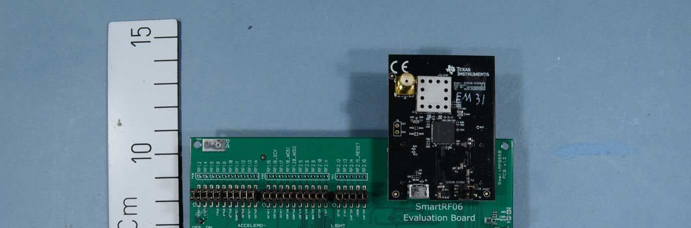
Click to zoom
Application Details
- Equipment Class
- DTS - Digital Transmission System
- Date of Grant
- Feb 23, 2014
- Application Purpose
- Original Equipment
- Date of Application
- Feb 23, 2014
- Equipment Note
- The CC2538-CC2592EM is a development tool for TIs 2.4 GHz CC2538 radio MCU and CC2592 RF front end
- Frequency Range
- 2405.00000000 - 2480.00000000
- Company
- Texas Instruments Inc.
- Country
- United States
Documents & Files
Document Text
Text extracted from the exhibit documents filed with the FCC. Open a document above to read the original.
Users Manual
February 2014 Web sites: www.ti.com/lprf E2E Forum: www.ti.com/lprf-forum Make sure to subscribe to the Low-Power RF Newsletter to receive information about updates to documentation, new product releases, and more. Sign up on the TI web pages. CC2538-CC2592 Evaluation Module Kit Quick Start Guide Opening the Box and Running the Packet Error Rate Test 1. Kit Contents 2 x CC2538-CC2592 Evaluation Modules The RF boards in this kit are FCC and IC certified and tested/comply with ETSI/R&TTE over temperature from 0 to 35°C. FCC/IC Regulatory Compliance FCC Part 15 Class A Compliant IC ICES-003 Class A Compliant 2. How to use the Modules The EMK is an add-on kit to supplement the CC2538DK with evaluation boards. The CC2538-CC2592EM boards can be plugged into the SmartRF06 Evaluation Board from Texas Instruments. This board is included in the CC2538DK and in the SmartRF06EBK. This board lets you run a packet error rate (PER) test, control the device from SmartRF™ Studio and it can be used as a development platform. It is also possible to connect the EM to other TI development boards with the appropriate connectors This guide will show how to use the modules together with SmartRF06EB. 3. CC2538-CC2592EM Overview 4. Plug the EM into the 06EB Insert a CC2538-CC2592EM board into the SmartRF06EB as shown above. NB! Make sure that the jumper on the upper row on the header on the CC2538- CC2592EM is connected. Caution! The kit contains ESD sensitive components. Handle with care to prevent permanent damage. 5. Power Options The CC2538-CC2592EM should be powered through the SmartRF06EB, which will supply a voltage from 2.1V to 3.6V to the daughter card. The SmartRF06EB can be powered in several different ways: USB (5V through USB plug) 2 x 1.5V AAA alkaline batteries External power supply (see below) Voltage regulators on the SmartRF06EB will set the on-board voltage to 2.1V or 3.3V. External Regulated Power Supply 1 Requirements: Nom Voltage: 2.1 to 3.3 VDC. MAX 3.6 VDC. Max Current: 1000 mA Efficiency Level V Warning! To minimize risk of injury or property damage, never use rechargeable batteries to power the board. 6. Select Power Source The power source is selected using the Source switch on the left hand side of the SmartRF06EB. In “USB” position, the EM is powered over USB, running at 3.3V. In “BAT” position, the board is powered from batteries or an external source, running at 2.1V. The 2.1V regulator can be bypassed by shorting the pins on the “regulator bypass” jumper. In this case, the EM is powered directly from the external source or batteries. Note that there should only be one active power source at any one time. Do not leave the EVM powered when unattended. 7. Welcome Screen Turn on power with the Main Power switch. You should now see the Texas Instruments logo and a short description of the buttons on the LCD. Pushing any of the five buttons on the board will take you to the main menu. NB! If you don’t see anything on the screen make sure the board is correctly powered (see step 5 and 6 above). 8. Select Board and Channel Start by selecting the plug-in board you have, either the CC2538EM or the combo board CC2538-CC2591EM. Then select which channel (frequency) to use. 9. Select Mode One of the boards must operate as a transmitter and the other as a receiver. Select transmitter on one board ... ... and receiver on the other board. 1 When using an external power supply, make sure it meets the listed requirements in addition to complying with applicable regional product regulatory and safety certification requirements such as UL, CSA, VDE, CCC, and PSE. Power Select Jumper 1-2: Vdd from EB 1-3: Vdd from USB Micro USB connector for testing USB on CC2538 Emulator LEDs USB 5V to 3.3V LDO 10-pin ARM Debug Connector 20-pin ARM-JTAG Connector PCB Antenna SMA connector for conducted RF testing (not enabled by default) CC2538 CC2592 (under shield) 10. Select RX Gain Mode On the receiver, select either high gain or low gain mode for the CC2592. The receiver is now ready to receive packets. Continue with the configuration of the transmitter. 11. Select TX Power On the transmitter, select desired output power. 12. Select Packet Rate Still on the transmitter, select the desired burst size, that is, the number of packets to transmit. Then select the packet rate. 13. Start Sending Packets The transmitter is now configured and in idle state. Sending packets is started and stopped by pressing the Select button. 14. PER Test Results On the receiver, the statistics window will show the error rate based on the number of lost or erroneous packets divided by the total number of packets that should have been received. 15. References Please visit www.ti.com and http://www.ti.com/tool/cc2538-CC2592emk http://www.ti.com/tool/cc2538dk The reference design for the evaluation board can be found here: http://www.ti.com/tool/cc2538-cc2592em-rd On the kit product page, you will find additional documentation, links to updated software examples and software tools like SmartRF Studio. You will also find a lot of information on the TI E2E forum at http://e2e.ti.com We hope that you will enjoy working with the CC2592 and CC2538 devices. 16. Troubleshooting It you are experiencing problems with this test, please check the following: Nothing is shown in the display! Make sure the board is powered correctly (see steps 5 and 6 above). Please visit the kit web page and check for updated SW and documentation. Updated SW can be downloaded to the device using IAR Embedded Workbench for ARM or SmartRF Flash Programmer. SmartRF™ Studio 1. Download and Install Before connecting SmartRF06EB to your PC, download and install SmartRF Studio from www.ti.com/smartrfstudio. 2. Launch SmartRF Studio After installing the tool, connect the EB to the PC using the USB cable and start SmartRF Studio. Select the “2.4 GHz” tab and click the refresh ("Find device") button in the lower right corner. Studio will now find the connected SmartRF06E…
Text truncated - open the document above for the full version.
Block Diagram
CC2538-CC2592EM CC2538 f = <2405MHz – 2480MHz> CTRL LNA PA FREQUENCY SYNTHESIZER f_internal = <4810MHz – 4960MHz> f_output = <2405MHz – 2480MHz> AAF LPF ADC ADC DAC DAC DEMODULATOR MODULATOR RADIO CONTROLLER AND DATA INTERFACE QI QI RF_N RF_P I Q I Q CLOCK MUX P D 6 P D 7 X O S C _ Q 2 X O S C _ Q 1 16MHz RC-OSC 32kHz RC-OSC 32MHz Crystal OSC 32.768kHz Crystal OSC ADC CLOCK CC2592
External Photos
INTERNAL PHOTOS Project no.: 251857 FCC ID: ZAT25382592EM Page 1 (2) INTERNAL PHOTOS – CC2538-CC2592EM CC2538-CC2592EM – PCB component side CC2538-CC2592EM – rear side INTERNAL PHOTOS Project no.: 251857 FCC ID: ZAT25382592EM Page 2 (2) CC2538-CC2592EM with evaluation board SmartRF06EB Evaluation board SmartRF06EB-rear side with 2xAAA batteries
ID Label/Location Info
Texas Instruments Norway AS Gaustadalléen 21 0349 Oslo Norway (+47) 23 36 98 00 (+47) 23 36 98 01 Page 1 of 1 Description of FCC/IC/CE marking on CC2538-CC2592EM The FCC/IC/CE labeling of the CC2538-CC2592EM is shown below. The required markings are printed in the silk layer directly on the circuit board.
Internal Photos
INTERNAL PHOTOS Project no.: 251857 FCC ID: ZAT25382592EM Page 1 (2) INTERNAL PHOTOS – CC2538-CC2592EM CC2538-CC2592EM – PCB component side CC2538-CC2592EM – rear side INTERNAL PHOTOS Project no.: 251857 FCC ID: ZAT25382592EM Page 2 (2) CC2538-CC2592EM with evaluation board SmartRF06EB Evaluation board SmartRF06EB-rear side with 2xAAA batteries
Operational Description
Texas Instruments Norway AS Gaustadalléen 21 0349 Oslo Norway (+47) 23 36 98 00 (+47) 23 36 98 01 Page 1 of 1 Technical Description The CC2538-CC2592EM is a development tool for IEEE 802.15.4 solutions in the 2.4 GHz ISM band. The CC2538 is a System-on-Chip solution tailored for 2.4 GHz ZigBee applications. CC2592 is a PA/LNA front end for radios operating in the 2.4 GHz frequency band The CC2538-CC2592EM board is equipped with a 2.4 GHz PCB antenna. The board does not have any form of housing or cover, other than an RF shield for the CC2592 chip. The CC2538-CC2592EM is an engineering development board and cannot be used in an end product. The wireless control protocol is based on IEEE 802.15.4 at 2.4 GHz. The frequency range is 2405MHz to 2480MHz, with 5MHz channel spacing. The PHY layer uses a DSSS technique with a chip rate of 2Mbps and a data rate of 250kbps. The modulation format is half sine shaped O-QPSK. The CC2592 LNA/PA has a single ended RF antenna terminal. On the CC2538-CC2592EM, this single ended terminal is connected to the antenna through a matching network to ensure a 50 ohm RF match at the antenna. The antenna gain is 3.3 dBi.
Parts List/Tune Up Info
Part ReferenceQuantityValuePCB PackageDescriptionMPNManufacturerPart Number C2 C522.2uF0603CAPACITOR, CERAMIC X5R, 2.2uF, 10V, -20%/+20%, -55DEGC/+85DEGC, 0603, SMDGRM188R61A225ME34DMURATA02-01132 C3 C4121uF0603CAPACITORS, CERAMIC, 1uF, 15%, X5R, 10V, 0603, SMDGRM188R61A105KA61DMURATA02-01389 C41DNMCAPACITOR, DO NOT MOUNT, 0603, SMD02-01324 C21 C31247pF0402CAPACITOR, CERAMIC C0G/NP0, 47pF, 50V, -5%/+5%, -55DEGC/+125DEGC, 0402, SMDGRM1555C1H470JA01DMURATA02-04366 C101 C151 C241 C331 C361 C391 C4317100nF0402CAPACITOR, CERAMIC X7R, 100nF, 6.3V, -10%/+10%, -55DEGC/+125DEGC, 0402, SMDGRM155R70J104KA01DMURATA02-02323 C28111nF0402CAPACITOR, CERAMIC X7R, 1nF, 50V, -10%/+10%, -55DEGC/+125DEGC, 0402, SMDGRM155R71H102KA01DMURATA02-02070 C321 C551 C561 C310841uF0402CAPACITOR, CERAMIC X5R, 1uF, 10V, -10%/+10%, -55DEGC/+85DEGC, 0402, SMDGRM155R61A105KE15DMURATA02-02381 C341 C351 C3106 C3131412pF0402CAPACITOR, CERAMIC C0G/NP0, 12pF, 50V, -5%/+5%, -55DEGC/+125DEGC, 0402, SMDGRM1555C1H120JA01DMURATA02-04168 C3921220pF0402CAPACITOR, CERAMIC C0G/NP0, 220pF, 50V, -5%/+5%, -55DEGC/+125DEGC, 0402, SMDGRM1555C1H221JA01DMURATA02-01276 C441 C451222pF0402CAPACITOR, CERAMIC C0G/NP0, 22pF, 50V, -5%/+5%, -55DEGC/+125DEGC, 0402, SMDGRM1555C1H220JA01DMURATA02-04373 C3101 C310322.2pF0402CAPACITOR, CERAMIC C0G/NP0, 2.2pF, 50V, -0.25pF/+0.25pF, -55DEGC/+125DEGC, 0402, SMDGRM1555C1H2R2CA01DMURATA02-04605 C310510.2pF0402CAPACITOR, CERAMIC C0G/NP0, 0.2pF, 50V, -5%/+5%, -55DEGC/+125DEGC, 0402, SMDGRM1555C1HR20BA01DMURATA02-04165 C310711nF0402CAPACITOR, CERAMIC C0G/NP0, 1nF, 50V, -5%/+5%, -55DEGC/+125DEGC, 0402, SMDCAPACITOR_0402_1nF_C0G/NP0_M_+/-5%_50VMANUFACTURER SELECTION02-04728 C3109 C3111 C31333DNMCAPACITOR, DO NOT MOUNT, 0402, SMD02-01321 C3110118pF0402CAPACITOR, CERAMIC C0G/NPO, 18pF, 50V, -55DEGC/+125DEGC, 0402, SMDGRM1555C1H180JA01DMURATA02-02407 C313211nF0402CAPACITOR, CERAMIC X7R, 1nF, 50V, -5%/+5%, -55DEGC/+125DEGC, 0402, SMDCAPACITOR_0402_1nF_X7R_M_+/-5%_50VManufacturer selection02-03019 FL1 FL22BLM18HE152SN10603FILTER, EMI, 1500@100MHz, -55DEGC/+125DEGC, 0603, SMDBLM18HE152SN1DMURATA04-00470 J111981568-1CONNECTOR, USB-B, 5 PINS, PITCH 0.65mm, SMD1981568-1Tyco06-02244 J31SMA-10V21-TGGCONNECTOR, COAX RF, STRAIGHT, FEMALE, 1 PIN, SMDSMA-10V21-TGGHUS-TSAN06-02188 L310114.7nH0402INDUCTOR, CHIP, 4.7nH, -0.3nH/+0.3nH, 0.3A, -55DEGC/+125DEGC, 0402, SMDLQG15HS4N7S02DMURATA03-06631 L310211nH0402INDUCTOR, CHIP, 1nH, -0.3nH/+0.3nH, 0.3A, -55DEGC/+125DEGC, 0402, SMDLQG15HS1N0S02DMURATA03-06607 L310412nH0402INDUCTOR, CHIP, 2nH, -0.3nH/ +0.3nH, 0.3A, -55DEGC/+125DEGC, 0402, SMDLQG15HS2N0S02DMURATA03-06525 L32311DNMINDUCTOR, DO NOT MOUNT, 0402, SMD03-01022 P1 P22SFM-110-02-S-D-A-K-TRCONNECTOR, HEADER, FEMALE, STRAIGHT, 2 ROWS, 20 PINS, PITCH 1.27mm, SMDSFM-110-02-SM-D-A-K-TRSAMTEC06-02251 P51BB02-HP041-KB3-060B00CONNECTOR, HEADER, STRAIGHT, MALE, 4 PINS, 2 ROWS, 2.54mm PITCH, SMDBB02-HP041-KB3-060B00GradConn Cable 06-02190 P61DNMCONNECTOR, HEADER, MALE, STRAIGHT, 1 ROW, 2 PINS, PITCH 2.54mm, PTH826629-2AMP TYCO ELECTRONICS CORPORATION06-00059 R1 R111 R121 R271 R442 R4526DNMRESISTOR, DO NOT MOUNT, 0402, SMD01-02475 R21 R312330402RESISTOR, THICK FILM, 33, -1%/+1%, 0.063W, 50V, -55DEGC/+155DEGC, 0402, SMDRK73H1ETTP33R0FKOA SPEER01-16853 R3211.5k0402RESISTOR, THICK FILM, 1.5k, -1%/+1%, 0.063W, 50V, -55DEGC/+155DEGC, 0402, SMDRK73H1ETTP1501FKOA SPEER01-16854 R28112.2k0402RESISTOR, THICK FILM, 2.2k, -1%/+1%, 0.063W, 50V, -55DEGC/+155DEGC, 0402, SMDRK73H1ETTP2201FKOA SPEER01-11503 R421156k0402RESISTOR, THICK FILM, 56k, -5%/+5%, 0.063W, 50V, -55DEGC/+155DEGC, 0402, SMDCRCW040256K0JNEDVISHAY01-01262 R441 R451200402RESISTOR, JUMPER, -55DEGC/+155DEGC, 0402, SMDRK73Z1ETTPKOA SPEER01-01784 R3051 R3061 R3071310k0402RESISTOR, THICK FILM, 10k, -5%/+5%, 0.063W, 50V, -55DEGC/+155DEGC, 0402, SMDCRCW040210K0JNEDVISHAY01-01244 R308113.9k0402RESISTOR, THICK FILM, 3.9k, -1%/+1%, 0.063W, 50V, -55DEGC/+155DEGC, 0402, SMDRESISTOR_0402_3.9k_+/-1%_50V_0.063W_M_+/-100PPMMANUFACTURER SELECTION01-12675 SC11BMIS-201-FMECHANICAL, FRAME, SMDBMIS-201-FLAIRD13-00503 SC21BMIS-201-CMECHANICAL, COVER, NOT APPLYBMIS-201-CLAIRD13-00502 U11CC2538SF53RTQTVQFN56IC, ANALOG, POWER SYSTEM-ON-CHIP FOR 2.4GHz IEEE 802.15.4 ZigBee, 2V TO 3.6V, -40DEGC/+125 DEGC, VQFN56, SMDCC2538SF53RTQTTEXAS INSTRUMENTS18-29079 U21TLV70233SOT23-5IC, ANALOG, LOW-DROPOUT REGLATOR, VIN:2V TO 5.5V, VOUT:3.3V, SOT23-5, SMDTLV70233DBVRTEXAS INSTRUMENTS18-28503 U31CC2592QFN16IC, ANALOG, 2.4GHz RF FRONT END, 2V TO 3.7V, QFN16, SMDCC2592TEXAS INSTRUMENTS18-28661 X1132MHzSMDCRYSTAL, OSCILATOR, 32MHz, 10pF, -10PPM/+10PPM, -40DEGC/+85DEGC, SMDFA-128 32MHz 10pF 10PPMEpson Toyocom12-00422 X2132.768kHzCRYSTAL, OSCILATOR, 32.768kHz, -20PPM/ + 20PPM, -40DEGC/ +85DEGC, 12.5pF, SMDFC-12M 32.768kHz 20ppmEpson Toyocom12-00430
RF Exposure Info
FCC ID: ZAT25382592EM MPE Calculation for FCC Uncontrolled Environment Formula from page 18 of OET Bulletin 65, Edition 97 -01 where: S = power density P = power input to the antennaG = power gain of the antenna in the direction of i nterest relative to an isotropic radiator R = distance to the center of radiation of the ante nna Source Based Time Averaged Duty Cycle is 100% in ca lculation below Maximum peak output power at antenna input terminal : 18.53 (dBm) Maximum peak output power at antenna input terminal : 0.071 (W) Maximum antenna gain: 2.94 (dBi) Maximum antenna gain: 1.968 (numeric) Prediction distance: 20 (cm) Prediction frequency: 2405 (MHz) Time Averaged Duty Cycle 100 % MPE limit for uncontrolled exposure at prediction f requency: 10.00 (W/m^2) Power density at prediction frequency: 0.0279 (mW/cm^2) Power density at prediction frequency: 0.279 (W/m^2) Maximum allowable antenna gain: 18.48 (dBi) Margin of Compliance: 15.54 (dB) 2 4 R PG S π =
Schematics
11 22 33 44 55 A A B B C C D D USB interface Place close to pin10 Place close to pin15 Place close to pin24 External pull-up resistordriven by PC0 EM connector 1 EM connector 2 Place close to pin55 Place close to pin33 Place close to pin36 Place close to pin 39, 40 and 41 Place close to pin43 Placeholder fora large capacitorif needed close topower supply Pinrow for GPIOs not availablefrom EM connector 1 and 2.Not mounted Mount eitherC3111 or C3110 = 18 pFto select SMA or PCB ant. USB_NUSB_P PC0PC1PC2PC3PC4PC5PC6PC7PD0PD1PD2PD3PD4PD5PA0PA1PA2PA3PA4PA5PA6PA7PB0PB1PB2PB3PB4PB5 PB6/JTAG_TDIPB7/JTAG_TDO PB6/JTAG_TDIPB7/JTAG_TDO JTAG_TCK JTAG_TMS nRESET PC0 PC5PC6PC7PA3PA2PA4PA5 PB0PB1PA0PA1PB2PB3PB4PB5 PC4 PA6PC0PC1 PD5PD0PD3PD1 USB_N PA7PD4 PD6PD7 PC2PC3 PD2 PD2PC2PC3 USB_P nReset PD7PD6 JTAG_TMSJTAG_TCK VDD_EB VDD_EB DVDD_USB DVDD_USB DVDD_USB VDD_CC2538VDD_CC2592 VDD_CC2538 VDD_CC2592 Title:Drawn:Checked:Size: Rev: Sheet: of Date: CC2538-CC2592EM 1 1 2.0.1 A3 Fredrik Kervel Thursday, January 09, 2014 Title:Drawn:Checked:Size: Rev: Sheet: of Date: CC2538-CC2592EM 1 1 2.0.1 A3 Fredrik Kervel Thursday, January 09, 2014 Title:Drawn:Checked:Size: Rev: Sheet: of Date: CC2538-CC2592EM 1 1 2.0.1 A3 Fredrik Kervel Thursday, January 09, 2014 C331100nF C341 12pF FIDU4 R4410 U3CC2592 PA_EN 5 LNA_EN 6 HGM 7 GND 1 GND 9 GND 12 GND 16 EGP/GND 17 VDD_PA 15 RF_N 2 RF_P 3 ANT 10 GND 11 VDD_LNA 13 BIAS 8 VDD_BIAS 14 GND 4 L3231 DNM 12 C2811nF R4510 L31042nH 1 2 FIDU2 P5 BB02-HP041-KB3-060B00 3 4 1 2 R281 2.2k C3103 2.2pF R30813.9k P1 SFM-110-02-S-D-A-K-TR 13579 1113151719 2468101214161820 C3108 1uF C5511uF R3051 10k C5 2.2uF C3211uF P2 SFM-110-02-S-D-A-K-TR 13579 1113151719 2468101214161820 SHIELD SHIELD VBUS D+ D- ID GND J1 2 4 1 3 6 7 8 9 5 10 11 R3061 10k C3101 2.2pF X2 32.768kHz 1 2 R3071 10k SC2BMIS-201-C R271 DNM C3106 12pF C31 47pF SC1 BMIS-201-F 1 2 3 4 5 6 7 8 R1DNM C3131 12pF R42156k L31021nH 1 2 C392220pF X1 32MHz 1 2 4 3 FIDU1 C3107 1nF C391100nF C3133DNM R452 DNM C4 DNM C441 22pF C151100nF R442 DNM C2 2.2uF C451 22pF FIDU3 A1 DN007 3 21 C41 1uF R21 33 L3101 4.7nH 12 J3SMA-10V21-TGG 1 23 45 R111DNM R321.5k C361100nF R31 33 C431100nF C3 1uF FL2 BLM18HE152SN1 1 2 FL1 BLM18HE152SN1 1 2 P6DNM 12 C3105 0.2pF C3110 18pF TLV70233U2 IN 1 GND 2 EN 3 NC 4 OUT 5 C241100nF C351 12pF FIDU6 C3132 1nF C5611uF C21 47pF C101100nF R121DNM U1CC2538SF53RTQT PB0 5 DVDD 24 nRESET 28 DCOUPL2 32 AVDD 33 R_BIAS 42 AVDD_GUARD 43 JTAG_TMS 46 JTAG_TCK 47 PB6 49 DGND_USB 1 USB_P 2 USB_N 3 DVDD_USB 4 DVDD 10 DVDD 15 XOSC32M_Q1 34 XOSC32M_Q2 35 AVDD 41 PD6/XOSC32K_Q1 44 PD7/XOSC32K_Q2 45 PB7 48 AVDD 36 RF_P 37 RF_N 38 AVDD 39 AVDD 40 PB5 50 PB4 51 PB3 52 PB2 53 PB1 54 DVDD 55 DCOUPL1 56 AGND 57 PA7 23 PA6 22 PA5 21 PA4 20 PA3 19 PA2 18 PA1 17 PA0 16 PC0 14 PC1 13 PC2 12 PC3 11 PC4 9 PC5 8 PC6 7 PC7 6 PD0 25 PD1 26 PD2 27 PD3 29 PD4 30 PD5 31 C3111DNM FIDU5 C3109DNM
Test Report
Report No. 251857-1 Template version: B Nemko Norway Nemko AS, Instituttveien 6, P.O. Box 96 Kjeller, 2027 Kjeller, Norway TEL +47 22 96 03 30 FAX +47 22 96 05 50 EMAIL [email protected] ENTERPRISE NUMBER NO974404532 nemko.com/no Test Report Product Zigbee System on Chip Evaluation Board Name and address of the applicant Texas Instruments Norway AS Gaustadalléen 21, NO-0349 Oslo, Norway Name and address of the manufacturer Texas Instruments Norway AS Gaustadalléen 21, NO-0349 Oslo, Norway Model CC2538-CC2592EM Rating 3.0Vdc Trademark Texas Instruments Serial number / Additional information Zigbee System on Chip Tested according to FCC Part 15.247 Digital Transmission Systems Industry Canada RSS-210, Issue 8 Low Power Licence-Exempt Radiocommunications Devices Order number 251857 Tested in period 2014.01.08 to 2014.01.10 Issue date 2014.02.05 Name and address of the testing laboratory Instituttveien 6 Kjeller, Norway FCC No: 994405 IC OATS: 2040D-1 TEL: (+47) 22 96 03 30 FAX: (+47) 22 96 05 50 Prepared by [G.Suhanthakumar] Approved by [Frode Sveinsen] This report shall not be reproduced except in full without the written approval of Nemko. Opinions and interpretations expressed within this report are not part of the current accreditation. This report was originally distributed electronically with digital signatures. For more information contact Nemko. TEST REPORT FCC Part 15.247 Report no.: 251857-1 FCC ID: ZAT25382592EM Nemko Norway, Instituttveien 6, Kjeller, Norway Page 2 (76) CONTENTS 1 INFORMATION ......................................................................................................................... 3 1.1 Test Item .................................................................................................................................... 3 1.2 Test Environment ....................................................................................................................... 4 1.2.1 Normal test condition ................................................................................................... 4 1.3 Test Engineer(s) ........................................................................................................................ 4 1.4 Test Equipment .......................................................................................................................... 4 2 TEST REPORT SUMMARY ...................................................................................................... 5 2.1 General ...................................................................................................................................... 5 2.2 Test Summary ........................................................................................................................... 6 2.3 Description of modification for Modification Filing ...................................................................... 6 2.4 Comments ................................................................................................................................. 6 2.5 Family List Rational ................................................................................................................... 6 3 TEST RESULTS ........................................................................................................................ 7 3.1 Power Line Conducted Emissions ............................................................................................. 7 3.2 Minimum 6 dB Bandwidth .......................................................................................................... 8 3.3 20 dB Bandwidth ...................................................................................................................... 12 3.4 Peak Power Output .................................................................................................................. 13 3.5 Spurious Emissions (Radiated)................................................................................................ 23 3.6 Power Spectral Density (PSD) ................................................................................................. 71 4 LIST OF TEST EQUIPMENT................................................................................................... 75 5 BLOCK DIAGRAM .................................................................................................................. 76 5.1 Power Line Conducted Emission ............................................................................................. 76 5.2 Test Site Radiated Emission .................................................................................................... 76 TEST REPORT FCC Part 15.247 Report no.: 251857-1 FCC ID: ZAT25382592EM Nemko Norway, Instituttveien 6, Kjeller, Norway Page 3 (76) 1 INFORMATION 1.1 Test Item Name : Texas Instruments FCC ID : ZAT25382592EM IC : 451H-25382592EM Model/version : CC2538-CC2592EM Serial number : - Hardware identity and/or version: - Software identity and/or version : - Frequency Range : 2405 – 2480 MHz Number of Channels : 16 Type of Modulation : 250kbps, O-QPSK (Digital) Conducted Output Power: 0.071 Watts (Peak) User Frequency Adjustment : None Type of Power Supply : 3.0V DC (2xAAA Battery) Antenna Connector : N/A Antenna type: PCB antenna Antenna Diversity Supported : No Desktop Charger : None Description of Test Item The CC2538-CC2592EM is a 2.4 GHz RF-transceiver evaluation module containing the CC2538 IEEE 802.15.4/ZigBee System-on-Chip and the CC2592 range extender. TEST REPORT FCC Part 15.247 Report no.: 251857-1 FCC ID: ZAT25382592EM Nemko Norway, Instituttveien 6, Kjeller, Norway Page 4 (76) 1.2 Test Environment 1.2.1 Normal test condition Temperature: 20.2 - 21.5 °C Relative humidity: 40 - 43 % Normal test voltage: 3.0 V DC The values are the limit registered during the test period. 1.3 Test Engineer(s) G.Suhanthakumar 1.4 Test Equipment See list of test equipment in clause 4. TEST REPORT FCC Part 15.247 Report n…
Text truncated - open the document above for the full version.
Test Setup Photos
TEST SET-UP PHOTOS Project no.: 251857 FCC ID: ZAT25382592EM Page 1 (1) PHOTOS OF TEST SET-UP Radiated emissions 1 – 25 GHz
Contact Information
Applicant
Marian Kost(Product Line Manager, Connectivity)
Technical Contact
Non-Technical Contact
Texas Instruments Norway ASMagnus Wines
Test Firm
Nemko ASFrode Sveinsen
Technical Specifications
| # | Rule Parts | Frequency Range | Power Output |
|---|---|---|---|
| 1 | 15C | 2.40 GHz - 2.48 GHz | 71.00 mW |
Other Applications from Texas Instruments Inc.
ZAT-2340R5MODA
Jan 30, 2026CC2340R5MODAN0MHAR
Equipment Class
DTS - Digital Transmission SystemZAT-1312PSIP-3
May 19, 2024CC1312PSIP
Equipment Class
DSS - Part 15 Spread Spectrum TransmitterZAT-1312PSIP-2
Jan 21, 2024CC1312PSIP
Equipment Class
DSS - Part 15 Spread Spectrum Transmitter
ZAT-1312PSIP-1
Jul 09, 2023CC1312PSIP
Equipment Class
DSS - Part 15 Spread Spectrum Transmitter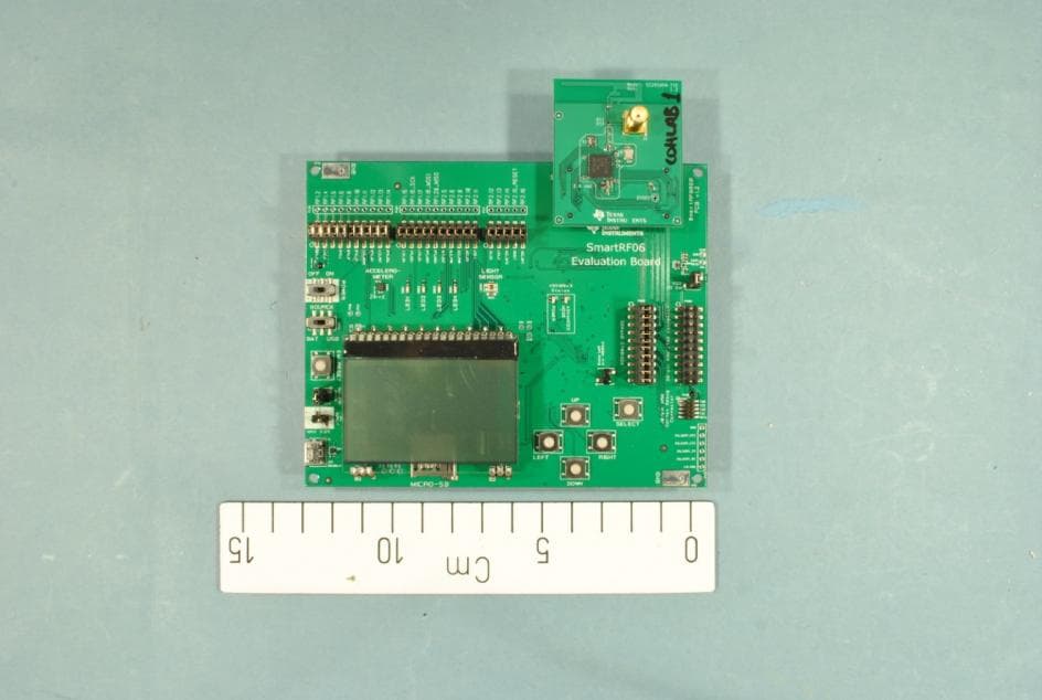
ZAT7IDEM
Feb 27, 2014The 7IDEM is a development tool for TIs 2.4 GHz 7ID System-on-Chip
Equipment Class
DTS - Digital Transmission System