ZAT2540EMThe CC2540EM is a development tool for TIs 2.4 GHz CC2540 Bluetooth low energy system-on-chip
Texas Instruments Inc.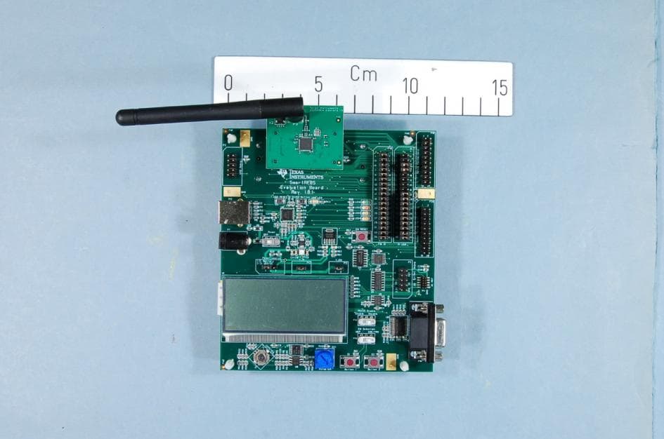
Click to zoom
Application Details
- Equipment Class
- DTS - Digital Transmission System
- Date of Grant
- Jan 16, 2014
- Application Purpose
- Original Equipment
- Date of Application
- Jan 16, 2014
- Equipment Note
- The CC2540EM is a development tool for TIs 2.4 GHz CC2540 Bluetooth low energy system-on-chip
- Frequency Range
- 2402.00000000 - 2480.00000000
- Company
- Texas Instruments Inc.
- Country
- United States
Documents & Files
Document Text
Text extracted from the exhibit documents filed with the FCC. Open a document above to read the original.
Users Manual
December 2013 Web sites: www.ti.com/ble E2E Forum: www.ti.com/ble-forum Make sure to subscribe to the Low-Power RF Newsletter to receive information about updates to documentation, new product releases, and more. Sign up on the TI web pages. CC2540 Evaluation Module Kit Quick Start Guide Opening the Box and Running the Bluetooth® Low Energy SimpleBLE Demo Application 1. Kit Contents 2 x CC2540 Evaluation Modules 2 x Pulse W1010 Antennas Documentation The kit is FCC and IC certified and tested/complies with ETSI/R&TTE over temperature from 0 to +35°C. The antenna, W1010 from Pulse, is a ¼ wave dipole antenna with 2 dBi gain. FCC/IC Regulatory Compliance FCC Part 15 Class A Compliant IC ICES-003 Class A Compliant 2. Hardware Requirements The CC2540EMK is an add-on kit to the CC2540DK. To run the example described in this Quick Start Guide, you would need two SmartRF05 Boards (Rev 1.8.1 or later). These boards are included in the CC2540DK (and not in the CC2540EMK). More information about the SmartRF05EB can be found in www.ti.com/lit/swru210. The CC2540EM boards can also be plugged into a battery board (see www.ti.com/tool/soc-bb) for standalone operation. 3. Hardware Setup Connect the antenna to the SMA connector on the CC2540 evaluation module (CC2540EM). Tighten the antenna’s screw firmly on to the SMA connector. If not properly connected, you might see reduced RF performance. Next, mount the CC2540EMs firmly on to connectors P5 and P6 on the SmartRF05EB. 4. Power Options There are several ways of applying power to the SmartRF05EB; USB (5V through USB plug) External Power Supply (see below) 2 x 1.5V AA Non-Rechargeable Alkaline Batteries Voltage regulators on the SmartRF05EB will set the on-board voltage to 3.3V. External Power Supply 1 Requirements: Nom Voltage: 4 to 20 VDC Max Current: 1500 mA Efficiency Level V Warning! To minimize risk of personal injury or property damage, never use rechargeable batteries to power the board. 5. Power the Boards Locate the power source header P11 just above the LCD on the SmartRF05EB. Connect pins 1 and 2 if you are using batteries to power the board. Connect pins 2 and 3 if you are using USB or external power supply. Once you have set P11, find switch P8 just next to the DC jack on the SmartRF05EB. To power on the board, flip the switch from “OFF” to “ON”. 6. Start-up Screen One of the CC2540EMs will be pre-loaded with the SimpleBLECentral application, while the other will be pre-loaded with the SimpleBLEPeripheral application. The LCD screens on the two SmartRF05EBs should display messages similar to those below: The “0x...” value displayed on each board is the device address. Every CC2540 device has a unique address. 7. Using the Joystick The SimpleBLEPeripheral application runs autonomously and does not require any user interaction. The SimpleBLECentral application, however, requires user interaction by means of joystick U1. Find joystick U1 on the top side of the SmartRF05EB, immediately below the LCD. The joystick has five different movements: it can be moved up, down, left, right, and it can be pressed in, just like a button. Each movement performs different actions depending on the state of the device. 8. Device Discovery Before the two devices can connect, the central device must first discover the peripheral device. To perform device discovery, press up on joystick U1 once. The LCD on the central device should display “Discovering...”. After a few seconds, it should display “Devices Found 1 / <- To Select”. This means that the central device successfully discovered the peripheral. Press left on joystick U1 to view the address of the peripheral device. This address should match the address seen on the peripheral’s LCD. 9. Establish Connection To establish a connection with the peripheral, press joystick U1 in towards the board (push it in like it is a button). Once the connection is established, the central device will automatically perform service discovery on the peripheral using the BLE GATT protocol. This should complete within a few seconds. The two LCD screens should appear as in the images below, with the central still displaying the peripheral’s address and the peripheral having changed from “Advertising” to “Connected”: Be careful that you don’t double tap U1 which would terminate the connection immediately, giving Disconnected Reason: 22. 1 When using an external power supply, make sure it meets the listed requirements in addition to complying with applicable regional product regulatory and safety certification requirements such as UL, CSA, VDE, CCC, and PSE. 10. Connected Operations Once the connection has been established and service discovery is complete, you can perform the following operations using joystick U1 on the central device: Read / Write Data – U1 UP RSSI Monitoring – U1 DOWN Connection Parameter Update – U1 RIGHT Terminate Link – U1 IN (towards the board) 11. Read / Write Data Pressing up on U1 will send a read request to the peripheral device. One byte of data will be read, and the value will be displayed. Pressing up again will send a write request, and one byte of data will be written to the peripheral. The peripheral’s LCD should display the written value each time this is done. Bluetooth low energy is an ideal technology for transmission of small amounts of data between two devices while consuming very little power, as is demonstrated here. Continuing to press up on the joystick will alternate between reads and writes, with the value incrementing each time. 12. Monitor RSSI Pressing down on U1 will turn on RSSI (received signal strength indication) monitoring. The RSSI will be displayed on the LCD in units of negative dBm. If the boards are moved farther apart from each other, the RSSI will drop (since the value is negative, a higher number means lower RSSI). If they are moved closer together, the RSSI should rise. Pressing down on U1 again will turn off RSSI monitoring. 13. Connection Param…
Text truncated - open the document above for the full version.
External Photos
INTERNAL PHOTOS Projectno.:215175 FCC ID:ZAT2540EM Page1(3) INTERNALPHOTOS–CC2540EM CC2540EM–PCB component side CC2540EM–rear side INTERNAL PHOTOS Projectno.:215175 FCC ID:ZAT2540EM Page2(3) Antenna CC2540EM with evaluation board SmartRF05EB INTERNAL PHOTOS Projectno.:215175 FCC ID:ZAT2540EM Page3(3) evaluation board SmartRF05EB-rear side with2xAA batteries
ID Label/Location Info
Certification Document Label 1/1 Description of label for CC2540EM FCC/IC/CE labeling of product is shown below. There is a separate label with the model name, optional variant designator, revision, serial number, FCC ID and IC number. Texas Instruments Model: CC2540EM (xx) Rev. x.x.x S.No.: xxxxxx FCC ID: ZAT2540EM IC: 451H-2540EM ~ 1 3 m m ~ 25 mm Placement of label on product ~ 40 mm ~ 3 3 m m T e x a s I n s t r u m e n t s M o d e l : C C 2 5 4 0 E M ( x x ) R e v . x . x . x S . N o . : x x x x x x F C C I D : Z A T 2 5 4 0 E M I C : 4 5 1 H - 2 5 4 0 E M Front Back Label manufacturer is Brady. Label part number B473 (http://www.bradyid.com/bradyid/domino/contentView.do/B473.html) with print using series R6000 ribbons (R6007 - http://www.bradyid.com/bradyid/pdpv/IP-R6007.html).
Internal Photos
INTERNAL PHOTOS Projectno.:215175 FCC ID:ZAT2540EM Page1(3) INTERNALPHOTOS–CC2540EM CC2540EM–PCB component side CC2540EM–rear side INTERNAL PHOTOS Projectno.:215175 FCC ID:ZAT2540EM Page2(3) Antenna CC2540EM with evaluation board SmartRF05EB INTERNAL PHOTOS Projectno.:215175 FCC ID:ZAT2540EM Page3(3) evaluation board SmartRF05EB-rear side with2xAA batteries
Operational Description
Texas Instruments Norway AS Gaustadalléen 21 0349 Oslo Norway (+47) 22 95 85 44 (+47) 22 95 85 46 Technical Description The CC2540EM is an evaluation board for the CC2540 RF SoC from Texas Instruments. The CC2540EM is preprogrammed with software that allows the user to create a simple Bluetooth® Low Energy (BLE) connection with another CC2540EM. Through one of the boards the user can read out the Received Signal Strength Indicator value, transfer simple key presses to the other board, and adjust certain BLE-specific connection parameters (not physical parameters such as output power; channel etc.). The CC2540 System on Chip has a differential RF output. On the CC2540EM board this differential output is transformed to a single ended, 50 ohm signal through a passive component (capacitor/inductor) balun. The output of the balun is low pass filtered to reduce harmonic radiation and then connected to an SMA connector. The antenna supplied with the board is W1010 from Pulse Electronics. The datasheet of the antenna is attached for further details.
Parts List/Tune Up Info
CC2540EM discrete 1.5.1 Mark assembled PCB "CC2540EM_D_R1.5.1" Use with PCB rev 1.5 2010-06-03: C_2U2_0402_X5R_M_4VDC replaced by C_2U2_0402_X5R_M_6p3VDC Ref. Part namePcs/unitDescriptionManufacturerPart numberSupplierOrdering code U1CC254012.4 GHz SoC TICC2540TICC2540 C2C_04020Capacitor, general, 0402; Do not mount C101;C211;C241;C271;C311C_100N_0402_X5R_K_105Capacitor, 100n, 0402, X5R, 10%, 10VMurataGRM155R71A104KA01D C221;C231C_12P_0402_NP0_J_502Capacitor, 12p, 0402, NP0, 5%, 50VMurataGRM1555C1H120JZ01D C321;C331C_15P_0402_NP0_J_502Capacitor, 15p, 0402, NP0, 5%, 50VMurataGRM1555C1H150JZ01D C251;C261C_18P_0402_NP0_J_502Capacitor, 18p, 0402, NP0, 5% 25VMurataGRM1555C1H180JZ01DELFA65-881-23 C201C_1N_0402_NP0_J_501Capacitor, 1n, 0402, NP0, 5%, 50VMurataGRM1555C1H102JA01D C252-253;C262C_1P0_0402_NP0_C_503Capacitor, 1p, 0402, NP0, +/-0.25pF 50VMurataGRM1555C1H1R0CZ01D C391;C401C_1U_0402_X5R_K_6P32Capacitor, 1u, 0402, X5R, 10%, 6.3VMurataGRM155R60J105KE19D C272C_220P_0402_NP0_J_501Capacitor, 220p, 0402, NP0, 5%, 50VMurataGRM1555C1H221JA01D C1C_2U2_0402_X5R_M_6p3VDC1Capacitor, 2u2, 0402, X5R, +/-20%, 6.3VMurataGRM155R60J225METTI L252L_1N0_0402_S1Inductor, 1n0, 0402, Monolithic type, +/-0.3 nHMurataLQG15HS1N0S02D L251;L261L_2N0_0402_S2Inductor, 2n0, 0402, +/-0.3 nHMurataLQG15HS2N0S02D L253L_3N0_0402_S1Inductor, 3n0, 0402, Monolithic type, +/-0.3 nHMurataLQG15HS3N0S02DACTE L1L_BEAD_102_04021EMI filter bead, 0402 1Kohms Tape GHz Band Gen UseMurataBLM15HG102SN1DACTE R1-4R_04020Resistor, general, 0402; Do not mount R201R_2K7_0402_F1Resistor, 2k7 ohms, 0402, ±1% KoaRK73H1ETTP2701F ELFA60-482-50 R301R_56K_0402_F1Resistor, 56k ohms, 0402, ±1% KoaRK73H1ETTP5602FELFA60-488-96 P3SMA_SMD1SMA connector, straight SMD-mountHus-Tsan Group TaiwanSMA-10V21-TGGEC Partner A/SSMA-10V21-TGG P1-2SMD_SOCKET_2x102SMD pinrow socket, .050 spacing, 2x10SamtecSFM-110-02-SM-D-A-K-TRAbacus X1X_32.000/10/20/60/101Crystal, 32 MHz, FA-128 -40/+85C, 10pF,Epson ToyocomFA-128, 32MHZ, 10PPM, 10PF, 2x1.6mm, -40/+85C,ACTEQ22FA1280009200 X2X_32.768/20/50/40/121Crystal, 32.768 kHz, 12.5pF, 20/50 ppm,SMD packageEpson ToyocomMC-306ACTEQ13MC3061000314 Total 32
RF Exposure Info
SAR Exclusion Justification Test exclusion thresholds for 100 MHz to 6 GHz at test separation distances ≤ 50 mm Guidance document reference: 447498 D01 General RF Exposure Guidance v05r01, page 11, paragraph 4.3.1(1). The 1-g and 10-g SAR test exclusion thresholds for 100 MHz to 6 GHz at test separation distances ≤ 50 mm are determined by: [(max. power of channel, including tune-up tolerance, mW)/(min. test separation distance, mm)] * [√f(GHz)] ≤ 3.0 for 1-g SAR and ≤ 7.5 for 10-g extremity SAR, where • f(GHz) is the RF channel transmit frequency in GHz • Power and distance are rounded to the nearest mW and mm before calculation • The result is rounded to one decimal place for comparison • 3.0 and 7.5 are referred to as the numeric thresholds in the step 2 below The test exclusions are applicable only when the minimum test separation distance is ≤ 50 mm and for transmission frequencies between 100 MHz and 6 GHz. When the minimum test separation distance is < 5 mm, a distance of 5 mm according to 5) in section 4.1 is applied to determine SAR test exclusion. SAR test exclusion analysis: Assumptions: Since the exact separation distance may vary from sensor to sensor, the minimum separation distance of 5 mm is assumed per the guidance document. Max. power of channel:3mW Min. separation distance:5 mm Max. frequency:2.48GHz [(Pwr/Dist)*√Freq.] = 0.9 The result of the above SAR threshold calculation demonstrates that the result is less than the 1-g numeric threshold of 3 and the 10-g numeric threshold of 7.5. Conclusion: The above analysis shows that the evaluated device qualifies for exemption from SAR testing. Signed: Tom Tidwell, Technical Manager 1/14/2013 Nemko USA, Inc.
Schematics
P2.1 P2.2 P1.0 P1.1 P0.7 P0.6 P0.3 P1.7 P1.6 P1.5 P1.4 P1.3 P0.1 VDD_FILT P0.4 P0.0 P0.2 VDD VDD 1 2 C201 C_1N_0402_NP0_J_50 12 34 56 78 910 1112 1314 1516 1718 1920 P1.2 P0.5 P2.0 P2 SMD_SOCKET_2X10 1 2 C391C_1U_0402_X5R_K_6P3 1 2 C221 C_12P_0402_NP0_J_50 1 2 C231 C_12P_0402_NP0_J_50 1 2 C1 C_2U2_0402_X5R_M_4VDC 1 2 C321 C_15P_0402_NP0_J_50 1 2 C101C_100N_0402_X5R_K_10 1 2 C311C_100N_0402_X5R_K_10 1 2 C2 C_0402 1 FM2 FIDUCIAL_MARK_1MM 1 FM4 FIDUCIAL_MARK_1MM 1 2 C252 C_1P0_0402_NP0_C_50 1 2 C262 C_1P0_0402_NP0_C_50 1 FM1 FIDUCIAL_MARK_1MM 1 2 C251 C_18P_0402_NP0_J_50 1 2 C271 C_100N_0402_X5R_K_10 1 2 C241 C_100N_0402_X5R_K_10 1 FM5 FIDUCIAL_MARK_1MM 1 2 C253 C_1P0_0402_NP0_C_50 1 2 C401 C_1U_0402_X5R_K_6P3 1 2 3 4 5 6 7 8 9 10 11 12 13 14 15 16 17 18 19 20 21 22 23 24 25 26 27 28 29 30 31 32 33 34 35 36 37 38 39 40 41 P0_5 P1_5 RBIAS AVDD2 P0_6 P0_7 P0_4 P1_6 P0_2 P1_7 P0_0 P0_1 P0_3 GND AVDD4 AVDD3 DCOUPL P1_0 P1_4 AVDD1 RESET_N P2_4 P1_1 P1_3 P1_2 RF_P P2_2 P2_3 P2_0 RF_N P2_1 DVDD1 DVDD2AVDD5 AVDD6 XOSC_Q1 XOSC_Q2 DGND_USB USB_P USB_N DVDD_USB U1 CC2540 1 2 34 56 78 910 1112 1314 1516 1718 1920 P0.4 P1.3 P0.1 P1.0 P0.2 P0.3P2.1 P0.0 P2.2 P1.1 P1.4 P0.6P1.5 P0.7 P1.6 P1.7 P1 SMD_SOCKET_2X10 1 2 C331 C_15P_0402_NP0_J_50 1 2 C261 C_18P_0402_NP0_J_50 1 2 C211C_100N_0402_X5R_K_10 1 2 C272 C_220P_0402_NP0_J_50 1 FM3 FIDUCIAL_MARK_1MM 1 2 3 45 P3 SMA_SMD 1 2 3 4 GND X1X_32.000/10/20/60/10 1 FM6 FIDUCIAL_MARK_1MM 12 L252 L_1N0_0402_S 12 L261 L_2N0_0402_S 1 2 L251 L_2N0_0402_S 12 L253 L_3N0_0402_S 12 L1 L_BEAD_102_0402 12 R201 R_2K7_0402_F 1 2 R301 R_56K_0402_F 1 2 R4 R_0402 1 2 R3 R_0402 12 R1 R_0402 12 R2 R_0402 1 4 X2X_32.768/20/50/40/12 TP3 TESTPOINT_CIRCLE_40MILS TP4 TESTPOINT_CIRCLE_40MILS TP1 TESTPOINT_CIRCLE_40MILS TP5 TESTPOINT_CIRCLE_40MILS TP2 TESTPOINT_CIRCLE_40MILS COMPANY NAME DWG DWG NO. out REV. DATE APPROVALS SHEETSCALE + 1.5.1 - For op-amp test P0.0 In + P0.1 In - P0.2 Output For comparator test P0.4 In - P0.5 In + A4 ISSUED CHECKED DRAWN FSCM NO.SIZE CONTRACT NO. Texas Instruments 1 (1) NN CC2540EM Discrete SVG
Test Report
Report No.215175-1 Template version: B Nemko Norway Nemko AS, Instituttveien 6, P.O. Box 96 Kjeller, 2027 Kjeller, Norway TEL+4722 96 03 30FAX+4722 96 05 [email protected] ENTERPRISE NUMBERNO974404532nemko.com/no Test Report Product CC2540EM Name and address of the applicant Texas Instruments Norway AS Gaustadalléen 21, NO-0349 Oslo, Norway Name and address of the manufacturer Texas Instruments Norway AS Gaustadalléen 21, NO-0349 Oslo, Norway Model CC2540EM Rating 3.0Vdc Trademark Texas Instruments Serial number / Additional information / Tested according toFCC Part 15.247 Digital Transmission Systems Industry Canada RSS-210, Issue 8 Low Power Licence-Exempt Radiocommunications Devices Order number 215175 Tested in period 2013.11.15to2013.11.18 Issue date 2013.12.10 Name and address of the testing laboratory Instituttveien 6 Kjeller, Norway FCC No: 994405 IC OATS: 2040D-1 TEL: (+47)22 96 03 30 FAX: (+47)22 96 05 50 Preparedby [G.Suhanthakumar]Approved by [Frode Sveinsen] This report shall not be reproduced except in full without the written approval of Nemko. Opinions and interpretations expressed within this report are not part of the current accreditation. This reportwas originally distributed electronically with digital signatures. For more information contact Nemko. TEST REPORT FCC Part 15.247 Report no.:215175-1 FCC ID:ZAT2540EM Nemko Norway, Instituttveien 6, Kjeller, NorwayPage2(59) CONTENTS 1INFORMATION.........................................................................................................................3 1.1Test Item....................................................................................................................................3 1.2Test Environment.......................................................................................................................4 1.2.1Normal test condition...................................................................................................4 1.3Test Engineer(s)........................................................................................................................4 1.4Test Equipment..........................................................................................................................4 2TEST REPORT SUMMARY......................................................................................................5 2.1General......................................................................................................................................5 2.2Test Summary...........................................................................................................................6 2.3Description of modification for Modification Filing......................................................................6 2.4Comments.................................................................................................................................6 2.5Family List Rational...................................................................................................................6 3TEST RESULTS........................................................................................................................7 3.1Power Line Conducted Emissions.............................................................................................7 3.2Minimum 6 dB Bandwidth..........................................................................................................8 3.320 dB Bandwidth......................................................................................................................12 3.4Peak Power Output..................................................................................................................13 3.5Spurious Emissions (Radiated)................................................................................................23 3.6Power Spectral Density (PSD).................................................................................................54 4LIST OF TEST EQUIPMENT...................................................................................................58 5BLOCK DIAGRAM..................................................................................................................59 5.1Power Line Conducted Emission.............................................................................................59 5.2Test Site Radiated Emission....................................................................................................59 TEST REPORT FCC Part 15.247 Report no.:215175-1 FCC ID:ZAT2540EM Nemko Norway, Instituttveien 6, Kjeller, NorwayPage3(59) 1INFORMATION 1.1TestItem Name :Texas Instruments FCC ID :ZAT2540EM IC :451H-2540EM Model/version :CC2540EM Serial number :- Hardware identity and/or version:Rev.:1.5.1.1 Software identity and/or version :- Frequency Range :2402–2480 MHz Number of Channels :16 Type of Modulation :250 kHz, GFSK (Digital) Conducted Output Power:2.85mW (Peak) User Frequency Adjustment :None Type of Power Supply : 3.0V DC (2xAABattery) Antenna Connector :SMA Antenna type:Pulse W1010, ¼-wave dipole Antenna Diversity Supported :No Desktop Charger :None Description of TestItem The CC2540EM RF-transceiver module is an evaluation board for the CC2540 System-on-Chip designed to operate in the 2.4 GHz ISM band. The CC2540 radio complies with the BLE PHY requirements. Exposure Evaluation The EUT is exempted from RF Exposure Evaluation. TEST REPORT FCC Part 15.247 Report no.:215175-1 FCC ID:ZAT2540EM Nemko Norway, Instituttveien 6, Kjeller, NorwayPage4(59) 1.2Test Environment 1.2.1Normal test condition Temperature: 21-22C Relative humidity:42-48% Normal test voltage:3.0VDC The values are the limit registered during the test period. 1.3Test Engineer(s) G.Suhanthakumar 1.4Test Equipment See listof test equipment in clause 4. TEST REPORT FCC Part 15.247 Report no.:215175-1 FCC ID:ZAT2540EM Nemko Norway, Instituttveien 6, Kjeller, NorwayPage5(59) 2TEST REPORT SUMMA…
Text truncated - open the document above for the full version.
Test Setup Photos
TEST SET-UPPHOTOS Projectno.:215175 FCC ID:ZAT2540EM Page1(2) PHOTOS OF TEST SET-UP Radiated emissions-< 30MHz, 10 meter RadiatedEmissions30-1000 MHz, 3 meter TEST SET-UPPHOTOS Projectno.:215175 FCC ID:ZAT2540EM Page2(2) Radiated emissions 1–25 GHz, 3 meter & 1 meter
Contact Information
Applicant
Marian Kost(Product Line Manager, Connectivity)
Test Firm
Nemko ASFrode Sveinsen
Technical Specifications
| # | Rule Parts | Frequency Range | Power Output |
|---|---|---|---|
| 1 | 15C | 2.40 GHz - 2.48 GHz | 2.85 mW |
Other Applications from Texas Instruments Inc.
ZAT-2340R5MODA
Jan 30, 2026CC2340R5MODAN0MHAR
Equipment Class
DTS - Digital Transmission SystemZAT-1312PSIP-3
May 19, 2024CC1312PSIP
Equipment Class
DSS - Part 15 Spread Spectrum TransmitterZAT-1312PSIP-2
Jan 21, 2024CC1312PSIP
Equipment Class
DSS - Part 15 Spread Spectrum Transmitter
ZAT-1312PSIP-1
Jul 09, 2023CC1312PSIP
Equipment Class
DSS - Part 15 Spread Spectrum Transmitter
ZAT7IDEM
Feb 27, 2014The 7IDEM is a development tool for TIs 2.4 GHz 7ID System-on-Chip
Equipment Class
DTS - Digital Transmission System