ZAT2540USBThe CC2540Dongle is a development tool for the 2.4 GHz CC2540 BLE System-on-Chip with USB from TI.
Texas Instruments Inc.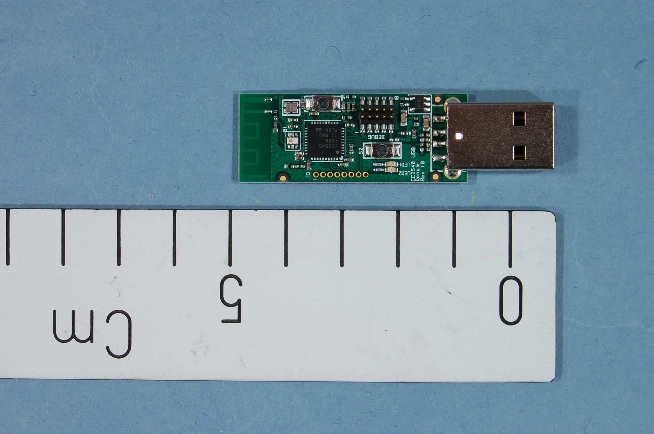
Click to zoom
Application Details
- Equipment Class
- DTS - Digital Transmission System
- Date of Grant
- Dec 05, 2012
- Application Purpose
- Original Equipment
- Date of Application
- Dec 04, 2012
- Equipment Note
- The CC2540Dongle is a development tool for the 2.4 GHz CC2540 BLE System-on-Chip with USB from TI.
- Frequency Range
- 2405.00000000 - 2480.00000000
- Company
- Texas Instruments Inc.
- Country
- United States
Documents & Files
Document Text
Text extracted from the exhibit documents filed with the FCC. Open a document above to read the original.
Users Manual
SWRU300 August2011 Web sites:www.ti.com/lprf E2E Forum:www.ti.com/lprf-forum Make sure to subscribe to the Low-Power RF Newsletter to receive information about updates to documentation, new product releases,and more. Sign up on the TI web pages. CC2540Development KitQuick StartGuide Opening the Box and Running theBluetooth®Low EnergySimpleBLEDemo Application 1. Kit Contents 2xSmartRF05EB (the two large boards) 2 x CC2540 Evaluation Modules 2 xPulse Antennas 1 xCC2540 USB Dongle Cables Documentation Please contact a TI Representative if any parts are missing from the kit. 2.Hardware Setup Connect the antennas to the SMA connector on the RF evaluation boards. Tighten the antenna’s screw firmly on to theSMA connector. If not properly connected, you might see reduced RF performance.Next,mounttheCC2540 evaluationmodules(CC2540EMs)onto connectors P5 and P6 on the SmartRF05EB. Make sure that the boards are pressed firmly into the connectors. 3.Power Options There are several ways of applying power to theSmartRF05EB. 2 x 1.5 V AABatteries USB External Power Supply For the batteries and USB, there are voltage regulators on theSmartRF05EBthat will set the on-board voltage to 3.3 V. The external power supply should set a voltage that does not exceed 3.3 V. Note that there should only be one active power source at any one time. 4. SetJumper P11 Find jumper P11 on the top side of each SmartRF05EB. This jumper is used to set the power source for the board. Set P11 to “1-2” if you are using battery power. Set P11 to “2-3” if you are using USB or an external power supply. 5.Turn on the Boards Once you have set P11, find switch P8 on the top sideof each SmartRF05EB. To power up the boards, flip the switch from the “OFF” position to “ON” 6.Start-up Screen One of the CC2540EMswill be pre-loaded with the SimpleBLECentral application, while the other will be pre-loaded with the SimpleBLEPeripheralapplication. The LCD screens on the two SmartRF05EBs should display messagessimilar to those below: The “0x...” value displayed on each board is the device address. Every CC2540 device hasa unique address. 7.Using the Joystick TheSimpleBLEPeripheralapplicationruns autonomously and does not require any user interaction. The SimpleBLECentral application, however,requires user interaction by means of joystick U1. Find joystick U1 on the top side of the SmartRF05EB, immediately below the LCD. The joystick has five different movements: it can be moved up, down, left, right, and it can pressed in like a button. Each movement performs different actions depending on the state of the device. 8.Device Discovery Beforethetwo devices can connect, thecentraldevice must first discover the peripheral device. To performdevice discovery, press up on joystick U1 once. The LCD on the central device should display “Discovering...”. After a few seconds, it should display “Devices Found 1 / <-To Select”. This means that the central device successfully discovered the peripheral. Press left on joystick U1 to view the address of the peripheral device. This address should match the address seen on the peripheral’s LCD. 9.Establish Connection Toestablisha connection with the peripheral,press joystickU1in towards the board (push it in like it is a button). Once the connectionis established,the central device will automatically perform service discovery on the peripheral using theBLEGATT protocol. This should complete within a fewseconds. The two LCD screens should appear as in the images below, with the central still displaying the peripheral’s addressand the peripheral havingchangedfrom“Advertising”to “Connected”: 10.Connected Operations Once the connection has been established and service discovery is complete, you can perform the following operations using joystick U1 on the central device: Read / Write Data–U1UP RSSI Monitoring–U1DOWN Connection Parameter Update–U1RIGHT Terminate Link–U1IN(towards the board) 11.Read / Write Data Pressing up on U1 will send a readrequest to the peripheral device. One byte of data will be read, and the value will be displayed. Pressing up again will send a write request, and one byte of data will be written to the peripheral. The peripheral’s LCD should display the written value each time this is done. Bluetoothlow energy is an ideal technology for transmission of small amounts of data between two deviceswhile consuming very little power, as is demonstrated here. Continuing to press up on the joystick will alternate between reads and writes, with the value incrementing each time. 12.Monitor RSSI Pressing down on U1 will turn on RSSI (received signal strength indication) monitoring. The RSSI will be displayed on the LCD in units of negative dBm. If the boards are moved farther apart from each other, the RSSI will drop (since the value is negative, a higher number means lower RSSI). If they are moved closer together, the RSSI should rise. Pressing down on U1 again will turn off RSSI monitoring. 13. Connection Parameter Update Pressingrighton U1 will send aconnection parameter update request to the peripheral to use a longer connection interval. This will result in much longer latency when performing data reads and writes; however the power consumed by both devices is significantly reduced. 14.Terminate Link Pressing U1 intowards the boardwill terminate the link. The peripheral will return to an advertising state.The central device willdisplay a “Reason” code, which indicates why the disconnection occurred (values are defined in the BLE stack API). In this case, the reason code of 22 indicates that the link termination was initiated by the central device. In the event that the peripheral device goes out of range or has power disconnected from it, you will see a reason code of8which indicates that a link timeout has occurred. You cannowperformdevice discovery and re- connect to the peripheralif desired. 15.SimpleBLE Demo Source Code The project and source codefilesfor these applications(as well as m…
Text truncated - open the document above for the full version.
Users Manual
October 2012 CC2540 USB Evaluation Kit Quick Start Guide 1. Kit Contents 1 x CC2540 USB Dongle 1 x Quick Start Guide The CC2540 USB Dongle in this kit is FCC and IC certified and tested to comply with ETSI/R&TTE over temperature from 0 to +35°C. Caution! The kit contains ESD sensitive components. Handle with care to prevent permanent damage. 2. Getting Started The CC2540 USB Dongle can be used as a development platform for USB and Bluetooth® low energy applications. The CC2540 USB Dongle in this kit comes preprogrammed with software that lets the dongle operate as a Bluetooth low energy packet capture device for the SmartRF™ Packet Sniffer. This Quick Start Guide will describe how to use the dongle with the packet sniffer and the next steps for your own software development. 3. Install the driver Before plugging the dongle into the PC, please install Texas Instruments’ SmartRF Packet Sniffer. When installing the Packet Sniffer, you will also automatically install the USB driver required for proper communication between the dongle and the packet sniffer. The SmartRF Packet Sniffer tool can be downloaded from the TI web at www.ti.com/tool/packet-sniffer 4. Insert the USB dongle When inserting the USB dongle into a USB slot, Windows’ new hardware wizard will appear. Select the options for automatic installation and wait for the driver installation to complete. After installation, the Packet Sniffer is ready for use. Caution! The CC2540 USB dongle is designed to be powered over USB, with a maximum voltage of 5.5V and maximum current of 500 mA. 5. Packet Sniffer TI’s SmartRF Packet Sniffer is a convenient tool for debugging of RF protocols. It displays the captured packets and decodes the packet contents depending on what protocol you are running. When starting the packet sniffer, select the protocol as required. The Packet Sniffer for CC2540 supports the Bluetooth low energy protocol. 6. SW Development For software development on the CC2540 an external debugger is necessary. This can be either a SmartRF05EB as shown in the first picture, ...or a CC Debugger [4] as shown in the second picture. October 2012 7. Flash Programmer Texas Instruments has a simple tool which can be used to program the flash on the CC2540. The Flash Programmer application, available on the kit web page [1], can be used to program Intel HEX files, read the contents of flash and several other operations. You will need a SmartRF05EB, a CC Debugger or other programmers from Third Parties [5] to program the device. 8. IAR Embedded Workbench To develop software and debug the code running on the CC2540, you should use IAR Embedded Workbench for 8051. IAR can also be used for programming. A free, code size limited version can be downloaded from the web. See www.iar.com/ew8051. 9. Thank You! We hope you will enjoy working with the CC2540 and associated Low- Power RF products from Texas Instruments. A. Available Software Bluetooth® low energy protocol stack Texas Instruments’ Bluetooth low energy stack can be downloaded from www.ti.com/blestack. SmartRF™ Studio SmartRF Studio can be used to test the performance for the CC2540 device and verify your RF design. Download from www.ti.com/smartrfstudio. B. More information On Texas Instruments’ Low-Power RF web site you will find all our latest products, application and design notes, FAQ section, news and events updates, and much more. Just go to www.ti.com/lprf The Low Power RF Online Community has forums, blogs and videos. Use the forums to find information, discuss and get help with your design. Join us at www.ti.com/lprf-forum The TI LPRF eNewsletter keeps you up to date on e.g. new products, application notes, software and events. Sign up at www.ti.com/lprfnewsletter C. References [1] CC2540EMK-USB web page www.ti.com/tool/cc2540emk-usb [2] CC2540 product web page www.ti.com/product/cc2540 [3] CC2540 Mini Kit www.ti.com/tool/cc2540dk-mini [4] CC Debugger www.ti.com/tool/cc-debugger [5] LPRF Developer’s Network www.ti.com/general/docs/gencontent.t sp?contentId=98994 EVALUATION BOARD/KIT/MODULE (EVM) ADDITIONAL TERMS Texas Instruments (TI) provides the enclosed Evaluation Board/Kit/Module (EVM) under the following conditions: The user assumes all responsibility and liability for proper and safe handling of the goods. Further, the user indemnifies TI from all claims arising from the handling or use of the goods. Should this evaluation board/kit not meet the specifications indicated in the User’s Guide, the board/kit may be returned within 30 days from the date of delivery for a full refund. THE FOREGOING LIMITED WARRANTY IS THE EXCLUSIVE WARRANTY MADE BY SELLER TO BUYER AND IS IN LIEU OF ALL OTHER WARRANTIES, EXPRESSED, IMPLIED, OR STATUTORY, INCLUDING ANY WARRANTY OF MERCHANTABILITY OR FITNESS FOR ANY PARTICULAR PURPOSE. EXCEPT TO THE EXTENT OF THE INDEMNITY SET FORTH ABOVE, NEITHER PARTY SHALL BE LIABLE TO THE OTHER FOR ANY INDIRECT, SPECIAL, INCIDENTAL, OR CONSEQUENTIAL DAMAGES. Please read the User's Guide and, specifically, the Warnings and Restrictions notice in the User's Guide prior to handling the product. This notice contains important safety information about temperatures and voltages. For additional information on TI's environmental and/or safety programs, please visitwww.ti.com/eshor contact TI. No license is granted under any patent right or other intellectual property right of TI covering or relating to any machine, process, or combination in which such TI products or services might be or are used. TI currently deals with a variety of customers for products, and therefore our arrangement with the user is not exclusive. TI assumes no liability for applications assistance, customer product design, software performance, or infringement of patents or services described herein. REGULATORY COMPLIANCE INFORMATION As noted in the EVM User’s Guide and/or EVM itself, this EVM and/or accompanying hardware may or may not be subject to the Federal Communications Commission (…
Text truncated - open the document above for the full version.
Block Diagram
f = <2400MHz – 2480MHz> CTRL LNA PA FREQUENCY SYNTHESIZER f_internal = <4800MHz – 4960MHz> f_output = <2400MHz – 2480MHz> AAF LPF ADCADCDACDAC DEMODULATOR MODULATOR RADIO CONTROLLER AND DATA INTERFACE Q I Q I RF_N RF_P I Q I Q CLOCK MUX P2_4 P2_3 XOSC_Q2 XOSC_Q1 16MHz RC-OSC 32kHz RC-OSC 32MHZ Crystal OSC 32.768kHz Crystal OSC BALUN ADC CLOCK
Cover Letter(s)
June 4, 2012 Nemko Canada Inc 303 River Road Ottawa, Ontario, Canada K1V 1H2 Attn: Director of Certification Authority to Act as Agent FCC On our behalf, I appoint Zarah MacIvor of Nemko USA, Inc. at 802 N Kealy Avenue, Lewisville TX 75057 to act as our agent in the preparation of this application for equipment certification. I certify that submitted documents properly describe the device or system for which equipment certification is sought. I also certify that each unit manufactured, imported or marketed, as defined in FCC regulations will have affixed to it a label identical to that submitted for approval with this application. In signing this letter, Applicant certifies that neither the applicant nor any party to the application is not subject to a denial of Federal benefits, that include FCC benefits, pursuant to Section 5301 of the Anti-Drug Abuse Act of 1988, 21 U.S.C. § 862 because of a conviction for possession or distribution of a controlled substance. See 47 CFR 1.2002(b) for the definition of a "party" for these purposes. For instances where our authorized agent signs the application for certification on our behalf, I acknowledge that all responsibility for complying with the terms and conditions for certification, as specified by Nemko Canada Inc, still resides with Texas Instruments, Inc., 12500 TI Boulevard, Dallas, TX 75243. Dated this 4th Day of June 20 12 Agency agreement expiration date: Usually Give 8 - 12 Months By: Signature Printed Title: On behalf of : (Company Name)
External Photos
FCC ID: / Project no.: 182239 Page 1 of 2 EXTERNAL PHOTOS – CC2540 USB Dongle
ID Label/Location Info
Certification Document Label 1/1 Description of label for CC2540Dongle FCC/IC/CE labeling of product is shown below. The CE logo is printed directly on the PCB. There is a separate label with the model name, optional variant designator, revision, serial number, FCC ID and IC number. Texas Instruments Model: CC2540Dongle (xx) Rev. x.x.x S.No.: xxxxxx FCC ID: ZAT2540USB IC: 451H-2540USB ~ 1 3 m m ~ 25 mm Placement of label on product 16 mm 4 1 m m 1 5 m m 11 mm T e x a s I n s t r u m e n t s M o d e l : C C 2 5 4 0 D o n g l e ( x x ) R e v . x . x . x S . N o . : x x x x x x F C C I D : Z A T 2 5 4 0 U S B I C : 4 5 1 H - 2 5 4 0 U S B
Internal Photos
FCC ID: / Project no.: 182239 Page 1 of 2 INTERNAL PHOTOS – CC2540 USB Dongle FCC ID: / Project no.: 182239 Page 2 of 2 USB Test-Jig with 3xAA cells
Operational Description
Texas Instruments Norway AS Gaustadalléen 21 0349 Oslo Norway (+47) 22 95 85 44 (+47) 22 95 85 46 Page 1 of 1 Technical Description The CC2540Dongle is an evaluation board for the CC2540 chip from Texas Instruments. The board is powered through USB. The CC2540Dongle included with the development kit can be used as a BLE sniffer and monitor packets while the SimpleBLE Demo is running.The SmartRF Protocol Packet Sniffer software can be downloaded from www.ti.com/packetsniffer. The CC2540 System on Chip has a differential RF output. On the CC2540Dongle board this differential output is transformed to a single ended, 50 ohm signal through an integrated balun from Johanson Technology (2450BM15A0002). Additionally the balun has integrated filter components which greatly reduces harmonic radiation. The single ended output of the balun is connected to an on-board PCB antenna.
Parts List/Tune Up Info
Ref. Part name Pcs/unit Description from PurchaseLib.xls Manufacturer Part number Supplier Ordering code Alt. Manufacturer Alt. Part number Alt. Supplier Alt. Ordering code Comments IO BL31_008U 1 U1 CC2540 1 2.4 GHz SoC TI CC2540 TI CC2540 C3 C_0402 1 Capacitor, general, 0402; Do not mount C5 C_0P5_0402_NP0_B_50 1 Capacitor, 0.5p, 0402, NP0, + /-0.1pF, 50V Murata GRM1555C1HR50BZ01D C101;C211;C241;C271;C311 C_100N_0402_X5R_K_10 5 Capaci tor, 100n, 0402, X5R, 10%, 10V Murata GRM155R71A104KA01D C41 C_10P_0402_NP0_J_50 1 Capacitor, 10p, 0402, NP0, 5 %, 50V Murata GRM1555C1H100JZ01D C221;C231 C_12P_0402_NP0_J_50 2 Capacitor, 12p, 0402, NP0, 5%, 50V Murata GRM1555C1H120JZ01D C201 C_1N_0402_NP0_J_50 1 Capacitor, 1n, 0402, NP0, 5% , 50V Murata GRM1555C1H102JA01D C391;C401 C_1U_0402_X5R_K_6P3 2 Capacitor, 1u, 0402, X 5R, 10%, 6.3V Murata GRM155R60J105KE19D C1 C_1U_0603_X5R_L_6P3 1 Capacitor, 1u, 0603, X5R, 15% , 6.3V Murata GRM188R60J105KA01D Farnell 4716607 C272 C_220P_0402_NP0_J_50 1 Capacitor, 220p, 0402, NP0 , 5%, 50V Murata GRM1555C1H221JA01D C4 C_2U2_0402_X5R_M_4VDC 1 Capacitor, 2u2, 0402, X5R, +/-20%, 4V Murata GRM1555C1H2R2CD01 C21;C31 C_47P_0402_NP0_J_50 2 Capacitor, 47p, 0402, NP 0, 5%, 50V Murata GRM1555C1H470JZ01D C2 C_4U7_0603_X5R_K_6 1 Capacitor, 4u7, 0603, X5R, 10% , 6.3V Murata GRM188R60J475KE19D FM1-3 FIDUCIAL_MARK_1MM 3 #N/A #N/A #N/A #N/A #N/A #N/A #N/A #N/A #N/A #N/A B1 2450BM15A0002 1 Balun, JTI matched ZIGBEE, 2400 ~ 2500 MHz, 2012-0 6 (EIA) 0805, SMD Johanson Technology 2450BM15A0002 Digikey 2450BM15A0002-ND D1 LED_EL19-21SURC 1 LED, red-orange, 0603, 2.0V, 39mc d Everlight 19-21SURC/S530-A2/TR8 ELFA 75-312-39 D2 LED_EL19-21SYGC 1 LED, green, 0603, 2.0V, 16mcd Everlight 19-21SYGC/S530-E1/TR8 ELFA 75-312-47 L301 L_6N8_0402_J 1 Inductor, 6n8, 0402, Monolithic ty pe, ±5% Murata LQG15HS6N8J02D L1 L_BEAD_102_0402 1 EMI filter bead, 0402 1Kohms Tape GHz Band Gen Use Murata BLM15HG102SN1D ACTE S1-2 SKRKAEE010 2 Tactile & Jog Switches 3.9x2.9x2.0mm Alps SKRKAEE010 Mouser 688-SKRKAE R2;R92 R_0402 2 Resistor, general, 0402; Do not mount R3;R9;R91 R_0_0402 3 Resistor, 0 ohm, 0402 Koa RK73Z1ETTP ELFA 60-470-05 R32 R_1K5_0402_G 1 Resistor, 1k5 ohms, 0402, 2% Koa RK73H1ETTP1501F (±1%) ELFA 60-481-36 R11;R71 R_270_0402_F 2 Resistor, 270 ohms, 0402, ±1% Koa RK73H1E270RF-MR or RK73H1ETTP2700F ELFA 60-885-61 or 60-477-73 R201 R_2K2_0402_G 1 Resistor, 2k2 ohms, 0402, 2% Koa RK73H1ETTP2201F (±1%) ELFA 60-482-19 R1 R_2_0402_F 1 Resistor, 2 ohms, 0402, ±1% Koa RK73H1ETTP2R00F R21;R31 R_33_0402_G 2 Resistor, 33 ohms, 0402, 2% Koa RK73H1ETTP33R0F (±1%) ELFA 60-473-36 R301 R_56K_0402_F 1 Resistor, 56k ohms, 0402, ±1% Koa RK73H1ETTP5602F ELFA 60-488-96 DEBUG STL21 1 10 pins connector MPE-Garry GmbH STL21-A01XX-010-TRU Freber U2 TPS76933 1 ULTRALOW-POWER 100-mA LOW-DROPOUT LINEAR REGULATORS TI TPS76933DBVR or -T P1 USB_A 1 USB Plugg A/PCB Montering ELFA 42-197-15 Freber CU01PAM10R0 AMP 787780-1 ELFA 42-707-40 X1 X_32.000/10/20/60/10 1 Crystal, 32 MHz, FA-128 -40 /+85C, 10pF, Epson Toyocom FA-128, 32MHZ, 10PPM, 10PF, 2x1.6mm, - 40/+85C, ACTE Q22FA1280009200 Total 47 CC2540 USB Dongle Parts List 1.0
RF Exposure Info
Prediction of MPE limit at a given distance Equation from page 18 of OET Bulletin 65, Edition 97-01 where:S = power density P = power input to the antenna G = power gain of the antenna in the direction of interest relative to an isotropic radiator R = distance to the center of radiation of the antenna Maximum peak output power at antenna input terminal:1.80(dBm)* Maximum peak output power at antenna input terminal:1.5(mW) Antenna gain(maximum):0(dBi)* Maximum antenna gain:1.00(numeric) Time Averaging:100(%)* Prediction distance:20(cm)* Prediction frequency:2450(MHz)* MPE limit for uncontrolled exposure at prediction frequency:1.000(mW/cm^2) Power density at prediction frequency:0.0003 (mW/cm^2) This equates to:0.003 W/m^2 2 4R PG S
Test Report
Nemko AS, Gaustadalléen 30, P.O.Box 73 Blindern, NO-0314 Oslo Norway T +47 22 96 03 30 F +47 22 96 05 50 Enterprise number NO974404532 Visiting address: Nemko Kjeller, Instituttveien 6, P.O.Box 96, NO-2027 Kjeller Norway T +47 64 84 57 00 F +47 64 84 57 05 Test report no. : 182239-5 Item tested : CC2540Dongle Type of equipment : 2.4GHz USB Dongle FCC ID : ZAT2540USB Client : Texas Instruments Norway AS FCC Part 15.247 Digital Transmission System RSS-210, Issue 8 Low Power Licence-Exempt Radiocommunication Devices 2012-05-29 Authorized by : .............................................. Geir Antonsen Technical Verificator TEST REPORT FCC part 15.247 Ref. no.: 182239-5 FCC ID: ZAT2540USB Nemko AS, NO-2027 Kjeller Page 2 (33) CONTENTS 1 GENERAL INFORMATION ...................................................................................................... 3 1.1 Testhouse Info .......................................................................................................................... 3 1.2 Client Information ...................................................................................................................... 3 1.3 Responsible Manufacturer (If other than client) ........................................................................ 3 2 Test Information ...................................................................................................................... 4 2.1 Test Item ................................................................................................................................... 4 2.2 Test Environment ...................................................................................................................... 5 2.3 Test Period................................................................................................................................ 5 3 TEST REPORT SUMMARY ..................................................................................................... 6 3.1 General ..................................................................................................................................... 6 3.2 Test Summary ........................................................................................................................... 7 3.3 Description of modification for Modification Filing ..................................................................... 7 3.4 Comments ................................................................................................................................ 7 3.5 Family List Rational .................................................................................................................. 7 4 TEST RESULTS ....................................................................................................................... 8 4.1 Power Line Conducted Emissions ............................................................................................ 8 4.2 Minimum 6 dB Bandwidth ....................................................................................................... 10 4.3 20 dB Bandwidth ..................................................................................................................... 11 4.4 Peak Power Output ................................................................................................................. 12 4.5 Spurious Emissions (Radiated) .............................................................................................. 15 4.6 Receiver Spurious Emissions ................................................................................................. 28 4.7 Power Spectral Density (PSD) ................................................................................................ 30 5 LIST OF TEST EQUIPMENT .................................................................................................. 32 6 BLOCK DIAGRAM ................................................................................................................. 33 6.1 Power Line Conducted Emission ............................................................................................ 33 6.2 Test Site Radiated Emission ................................................................................................... 33 TEST REPORT FCC part 15.247 Ref. no.: 182239-5 FCC ID: ZAT2540USB Nemko AS, NO-2027 Kjeller Page 3 (33) 1 GENERAL INFORMATION 1.1 Testhouse Info Name : Nemko AS Address : Nemko Kjeller Instituttveien 6, Box 96 NO-2027 Kjeller, NORWAY Telephone : +47 64 84 57 00 Fax : +47 64 84 57 05 E-mail: [email protected] FCC test firm : 994405 IC OATS : 2040D-1 Total Number of Pages: 33 1.2 Client Information Name : Texas Instruments Norway AS Address : Gaustadalléen 21, NO-0349 Oslo, Norway Telephone : +47 22 95 85 44 Fax : +47 22 95 85 46 Contact: Name : Fredrik Kervel Telephone : +47 22 95 8362 E-mail : [email protected] 1.3 Responsible Manufacturer (If other than client) Name : / Address : / TEST REPORT FCC part 15.247 Ref. no.: 182239-5 FCC ID: ZAT2540USB Nemko AS, NO-2027 Kjeller Page 4 (33) 2 Test Information 2.1 Test Item Name : Texas Instruments FCC ID : ZAT2540USB Model/version : CC2540Dongle Serial number : / Hardware identity and/or version: / Software identity and/or version : / Frequency Range : 2405 – 2480 MHz Number of Channels : 16 Type of Modulation : Digital User Frequency Adjustment : None Type of Power Supply : Powered from USB Antenna Connector : None (PCB Antenna) Antenna Diversity Supported : No Desktop Charger : None Description of Test Item The tested EUT is a 2.4GHz transceiver on a USB Dongle. Exposure Evaluation The EUT is exempted from RF Exposure Evaluation. TEST REPORT FCC part 15.247 Ref. no.: 182239-5 FCC ID: ZAT2540USB Nemko AS, NO-2027 Kjeller Page 5 (33) 2.2 Test Environment 2.2.1 Normal test condition Temperature: 20 - 22 °C Relative humidity: 42 - 52 % Normal test voltage: 4.5 V DC The radiated emissions tests were performed with the EUT powered from a t…
Text truncated - open the document above for the full version.
Test Setup Photos
FCC ID: / Project no.: 182239 Page 1 of 2 PHOTOS OF TEST SET-UP – CC2540 USB Dongle Radiated Emissions 30 - 1000 MHz Radiated Emissions 1 - 12 GHz FCC ID: / Project no.: 182239 Page 2 of 2 Power line Conducted Emissions Test
Contact Information
Applicant
Marian Kost(Product Line Manager, Connectivity)
Technical Contact
Non-Technical Contact
Nemko USA, Inc.Zarah G MacIvor
[email protected]214-629-5683
Test Firm
Nemko ASFrode Sveinsen
Technical Specifications
| # | Rule Parts | Frequency Range | Power Output |
|---|---|---|---|
| 1 | 15C | 2.40 GHz - 2.48 GHz | 1.80 mW |
Other Applications from Texas Instruments Inc.
ZAT-2340R5MODA
Jan 30, 2026CC2340R5MODAN0MHAR
Equipment Class
DTS - Digital Transmission SystemZAT-1312PSIP-3
May 19, 2024CC1312PSIP
Equipment Class
DSS - Part 15 Spread Spectrum TransmitterZAT-1312PSIP-2
Jan 21, 2024CC1312PSIP
Equipment Class
DSS - Part 15 Spread Spectrum Transmitter
ZAT-1312PSIP-1
Jul 09, 2023CC1312PSIP
Equipment Class
DSS - Part 15 Spread Spectrum Transmitter
ZAT7IDEM
Feb 27, 2014The 7IDEM is a development tool for TIs 2.4 GHz 7ID System-on-Chip
Equipment Class
DTS - Digital Transmission System