ZAT2541EMThe CC2541EM is a development tool for TI�s 2.4 GHz CC2541 Bluetooth� Low Energy System-on-Chip.
Texas Instruments Inc.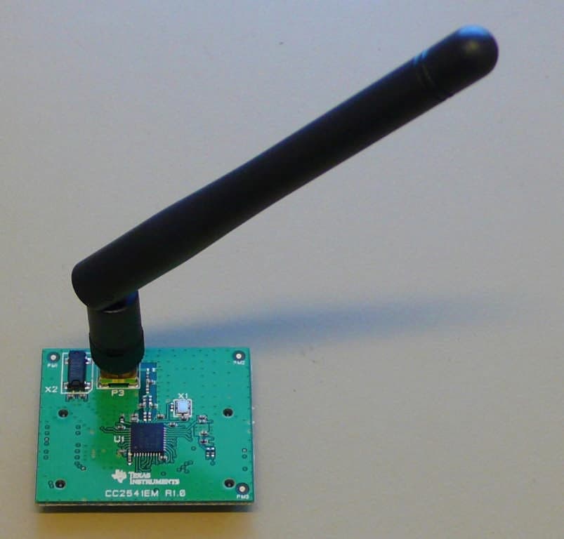
Click to zoom
Application Details
- Equipment Class
- DTS - Digital Transmission System
- Date of Grant
- Jan 17, 2012
- Application Purpose
- Original Equipment
- Date of Application
- Jan 16, 2012
- Equipment Note
- The CC2541EM is a development tool for TI�s 2.4 GHz CC2541 Bluetooth� Low Energy System-on-Chip.
- Frequency Range
- 2402.00000000 - 2480.00000000
- Company
- Texas Instruments Inc.
- Country
- United States
Documents & Files
Document Text
Text extracted from the exhibit documents filed with the FCC. Open a document above to read the original.
Users Manual
SWRU311 December2011 Web sites:www.ti.com/lprf E2E Forum:www.ti.com/lprf-forum Make sure to subscribe to the Low-Power RF Newsletter to receive information about updates to documentation, new product releases,and more. Sign up on the TI web pages. CC2541Evaluation ModuleKitQuick StartGuide Opening the Box and Running theBluetooth®Low EnergySimpleBLEDemo Application 1. Kit Contents 2 x CC2541Evaluation Modules 2 xPulseW1010Antennas Documentation ThekitisFCCandICcertifiedand tested/complieswithETSI/R&TTEover temperaturefrom0 to +35°C. The antenna, W1010 from Pulse,is a ¼ wave dipole antenna with 2 dBi gain. Caution!Thekit containsESD sensitive components. Handle with care to prevent permanent damage. 2.HardwareRequirements The CC2541EMK is an add-on kit to the CC2540DK. To run the example described in this Quick Start Guide, you would needtwo SmartRF05 Boards (Rev 1.8.1 or later). These boards are included in the CC2540DK (and not in the CC2541EMK). More information about the SmartRF05EB can be found inwww.ti.com/lit/swru210. The CC2541EM boards canalsobe plugged into a battery board (seewww.ti.com/tool/soc- bb) forstandalone operation. 3.HardwareSetup Connect the antenna to the SMA connector on the CC2541 evaluation module (CC2541EM). Tighten the antenna’s screw firmly on to the SMA connector. If not properly connected, you might see reduced RF performance. Next, mount the CC2541EMs firmly on to connectors P5 andP6onthe SmartRF05EB. Caution!To minimize risk of injury, avoid touchingcomponentsduringoperationif symbolized as hot. 4.Power Options There are several ways of applying power to the SmartRF05EB. 2 x 1.5 V AAAlkalineBatteries USB External Power Supply For the batteries and USB, there are voltage regulators on the SmartRF05EB that will set the on-board voltage to 3.3 V. The external power supply should set a voltage that does not exceed 3.3 V.Note that there should only be one active power source at any one time. Warning!To minimize risk of personal injury or property damage, never use rechargeable batteries to power the board. 5.Power the Boards Find jumper P11 on the top side of each SmartRF05EB. This jumper is used to set the power source for the board. Set P11 to “1-2” if you are using battery power. Set P11 to “2-3” if you are using USB or an external power supply. Once you have set P11, find switch P8 on the top sideofeach SmartRF05EB. To power up the boards, flip the switch from the “OFF” position to “ON”. DonotleaveEVMpoweredwhen unattended. 6.Start-up Screen One of the CC2541EMswill be pre-loaded with the SimpleBLECentral application, while the other will be pre-loaded with the SimpleBLEPeripheral application. The LCD screens on the two SmartRF05EBs should display messagessimilar to those below: The “0x...” value displayed on each board is the device address. EveryCC2541device hasa unique address. 7.Using the Joystick TheSimpleBLEPeripheralapplicationruns autonomously and does not require any user interaction. The SimpleBLECentral application, however,requires user interaction by means of joystick U1. Find joystick U1 on the top side of the SmartRF05EB, immediately below the LCD. The joystick has five different movements: it can be moved up, down, left, right, and it canbe pressed in, justlike a button. Each movement performs different actions depending on the state of the device. 8.Device Discovery Before the two devices can connect, the central devicemustfirst discover the peripheral device.Toperform device discovery, press up on joystick U1 once. The LCD on the central device should display “Discovering...”. After a few seconds, it should display “Devices Found 1 / <-To Select”. This means that the central device successfully discovered the peripheral. Press left on joystick U1 to view the address of the peripheral device. Thisaddress should match the address seen on the peripheral’s LCD. 9.Establish Connection Toestablisha connectionwith theperipheral, press joystick U1 intowardsthe board (push it in like it is a button). Oncethe connectionis established,thecentraldevicewill automatically perform service discovery on the peripheral using theBLEGATT protocol. This should complete within a fewseconds. The two LCD screens should appear as in the images below, with the central still displaying the peripheral’s addressand the peripheral havingchangedfrom“Advertising”to “Connected”: Be careful that you don’t double tap U1 which would terminate the connection immediately, givingDisconnected Reason: 22. 10.Connected Operations Once the connection has been established and service discovery is complete, you can perform the following operations using joystick U1 on the central device: Read / Write Data–U1UP RSSI Monitoring–U1DOWN Connection Parameter Update–U1RIGHT Terminate Link–U1IN(towards the board) 11.Read / Write Data Pressing up on U1 will send a read request to the peripheral device. One byte of data will be read, and the value will bedisplayed. Pressing up again will send a write request, and one byte of data will be written to the peripheral. The peripheral’s LCD should display the written value each time this is done. Bluetoothlow energy is an ideal technology for transmission of small amounts of data between two deviceswhile consuming very little power, as is demonstrated here. Continuing to press up on the joystick will alternate between reads and writes, with the value incrementing each time. 12.Monitor RSSI Pressing down on U1 will turn on RSSI (received signal strength indication) monitoring. The RSSI will be displayed on the LCD in units of negative dBm. If the boards are moved farther apart from each other,the RSSI will drop (since the value is negative, a higher number means lower RSSI). If they are moved closer together, the RSSI should rise. Pressing down on U1 again will turn off RSSI monitoring. 13. Connection Parameter Update Pressingrighton U1 will send aconnection parameter update request to the peripheral to use a longer connection interval. Th…
Text truncated - open the document above for the full version.
Block Diagram
Texas Instruments Norway AS Gaustadalléen 21 N-0349 Oslo, Norway Tel: +47 22 95 85 44 Fax: +47 22 95 85 46 CC2541 Block Diagram: Texas Instruments Norway AS Gaustadalléen 21 N-0349 Oslo, Norway Tel: +47 22 95 85 44 Fax: +47 22 95 85 46 CC2541 Frequencies: The following clocks contain both external and internal components: - 32 MHz crystal oscillator - 32.768 kHz crystal oscillator Internal clocks: - 16 MHz RC oscillator - 32 kHz RC oscillator - Frequency Synthesizer (2x RF carrier frequency): <4788 MHz – 5014 MHz>
Block Diagram
P 2 _ 4 P 2 _ 3 X O S C _ Q 2 X O S C _ Q 1
External Photos
FCC Certification Document Pictures 1/1 Internal PicturesofCC2541EM CC2541EM FrontCC2541EMBackside CC2541EMwith antenna
External Photos
FCC ID: ZAT2541EM Project no.: 182221 Page 1 of 2 INTERNAL PHOTOS – CC2541EM with SmartRF05EB CC2541EM FCC ID: ZAT2541EM Project no.: 182221 Page 2 of 2 Test Jig with 2xAA Batteries
ID Label/Location Info
FCC Certification Document Label 1/1 Description of Label for CC2541EM Label Placement of label on product(backside) ~ 3 3 m m T e x a s I n s t r u m e n t s C C 2 5 4 1 E M ( x x x ) R e v . x . x . x S . N o . : x x x x x x F C C I D : Z A T 2 5 4 1 E M I C : 4 5 1 H - 2 5 4 1 E M Information about label and labelmaterial: Label manufacturer is Brady. Specific part info: Label part number B473 (http://www.bradyid.com/bradyid/domino/contentView.do/B473.html). We use series R6000 ribbons(R6007-http://www.bradyid.com/bradyid/pdpv/IP-R6007.html). See following pages for relevant datasheet information. FCC Certification Document Label-Appendix i/vi Technical Data Sheet BRADY B-473 THERMAL TRANSFER PRINTABLE GLOSSY WHITE STATIC DISSIPATIVE POLYESTER LABEL STOCK TDS No. B-473 Effective Date: 26-Sep-2006 Description: GENERAL PrintTechnology:Thermal Transfer Material Type:White Polyester Finish:Glossy Adhesive:Static Dissipative Permanent Acrylic APPLICATIONS Printed circuit board and electronic component post-process labeling RECOMMENDED RIBBONS Brady Series R6000 REGULATORY/AGENCY APPROVALS UL:B-473 is a UL Recognized Component to UL969 Labeling and Marking Standard when printed with Brady Series R6000 ribbon. See UL file MH17154 for specific details. UL information can be accessed online atUL.com. Search inCertificationsarea. CSA:B-473 is CSA Accepted toC22.2 No. 0.15-95 Adhesive Labels Standard when printed with theBrady Series R6000 ribbon. See CSA file 041833 for specific details. CSA information can be accessed online atdirectories.csa-international.org. SP Provning Forskning:ESD-approved for IEC 61340-5-1 and EN 100015-1 per SP Swedish National Testing and Research Institute (see ESD-approval DNo: 230-02-0034). Brady B-473 is RoHS complinat to 2005/618/EC MCV amendment to RoHS Directive 2002/95/EC. SPECIAL FEATURES B-473 has a static dissipative adhesive and is supplied on a static dissipative release liner. It has surface resistivity values in the recommended range for Dissipative ESD Packaging Materials as defined in Table 1 of ANSI/ESD S20.20 (x10 5 to < 1x10 12 ohms). B-473 also meets the requirements of EIA-541 "Packaging Material Standards for ESD Sensitive Items" in which a charged material must decay to 1% of its initial voltage in less than 2 FCC Certification Document Label-Appendix ii/vi seconds. Details: PHYSICAL PROPERTIESTESTMETHODSAVERAGE RESULTS ThicknessASTM D 1000 -Substrate -Adhesive -Total 0.0020 inch (0.05 mm) 0.0014 inch (0.04 mm) 0.0034 inch (0.09 mm) Adhesion to: -Stainless Steel ASTM D 1000 20 minute dwell 24 hour dwell 49 oz/inch (54 N/100 mm) 60 oz/inch(66 N/100 mm) TackASTM D 2979 Polyken™Probe Tack (1 second dwell, 1 cm/sec separation) 31 oz (885 g) Drop ShearPSTC-7 (except use 1/2" x 1" sample) 70 hours Tensile Strength and Elongation ASTM D 1000 -Machine -Cross 38 lbs/inch (665N/100 mm), 68% 56 lbs/inch (980N/100 mm), 46% Dielectric StrengthASTM D 10009000 volts ELECTRICAL PROPERTIES TEST METHODSAVERAGE RESULTS Surface Resistivity- Adhesive EOS/ESD S11.11 -adhesive 5 x 10 8 ohms/sq. Liner Surface ResistivityEOS/ESD S11.11 -Release side -Backside 1.7 x 10 10 ohms/sq 2.5x 10 9 ohms/sq Static Decay-AdhesiveEIA-541 to 1% of initial charge 0.01 seconds Static Decay-LinerEIA-541 to 1% of initial charge -Release side 0.2 seconds Voltage (Label removed from liner, adhesive tested) Value is obtained by removing a 1.5" x 0.25" label from liner and immediately holding label to a static sensing device calibrated in volts. 10 volts FCC Certification Document Label-Appendix iii/vi Voltage (Label removed from liner, liner tested) Value is obtained by removing a labelfrom liner and immediately holding label to a static sensing device calibrated in volts. 3.4 volts The following testing was performed with B-473 thermal transfer printed on a BradyPrinter™THT 300X using a Brady Series R6000 ribbon. Labels printed with 3:1 ratio barcodes with 6 mil X dimension bars and alphanumerics. Samples laminated to aluminum panels and allowed to dwell 24 hours prior to testing. PERFORMANCE PROPERTIES TEST METHODTYPICAL RESULTS Short Term High Service Temperature 5 minutes at354°F (180°C)No visible effect to label at 180°C. Slight film shrinkage at 190°C but label is still functional. At 210°C label has severe film shrinkage. Long Term High Service Temperature 30 days at 248°F (120°C)No visible effect at 120°C Low ServiceTemperature30 days at-40°F (-40°C)No visible effect at-40°C Humidity Resistance30 days at 100°F (37°C) and 95% R.H. No visible effect UV Light Resistance30 days in UV Sunlighter™ 100 No visible effect Weatherability 1 ASTM G155, Cycle 1 30 days inXenon Arc Weatherometer No visible effect Salt Fog ResistanceASTM B 117 30 days in 5% salt fog solution chamber No visible effect PERFORMANCE PROPERTYCHEMICAL RESISTANCE Samples printed with Series R4900 and R6000 ribbons using a BradyPrinter™Model 300X. Labels printed with 3:1 ratio barcodes with 6 mil narrow X dimension bars and alphanumerics. Test was conducted at room temperature after 24 hour dwell. Testing consisted of 5 cycles of 10 minute immersions in the specified chemicals followed by a 30 minute recovery period. Samples rubbed 10 times with cotton swab immersed in test fluid after final immersion. CHEMICAL REAGENT SUBJECTIVE OBSERVATION OF VISUAL CHANGE LABEL STOCKR4900R6000EFFECT OF COTTON SWAB RUBS FCC Certification Document Label-Appendix iv/vi Methyl Ethyl Ketone Slightadhesive ooze No visible effectNo visible effectPrinting removed 1,1,1- Trichloroethane Slight adhesive ooze No visible effectNo visible effectPrinting removed TolueneSlight adhesive ooze No visible effectNo visible effectPrinting removed Freon®TMSSlight adhesive ooze No visible effectNo visible effectNo visible effect Isopropyl AlcoholNo visible effectNo visible effectNo visible effectNo visible effect Mineral SpiritsNo visible effectNo visible effectNo visible effectNo visibleeffect JP-4 Jet FuelNo visible effectNo visible effectNo visible ef…
Text truncated - open the document above for the full version.
Internal Photos
FCC Certification Document Pictures 1/1 Internal PicturesofCC2541EM CC2541EM FrontCC2541EMBackside CC2541EMwith antenna
Internal Photos
FCC ID: ZAT2541EM Project no.: 182221 Page 1 of 2 INTERNAL PHOTOS – CC2541EM with SmartRF05EB CC2541EM FCC ID: ZAT2541EM Project no.: 182221 Page 2 of 2 Test Jig with 2xAA Batteries
Operational Description
Texas Instruments Norway AS Gaustadalléen 21 N-0349 Oslo, Norway Tel: +47 22 95 85 44 Fax: +47 22 95 85 46 Technical Description The CC2541EM is an evaluation board for the CC2541 chip from Texas Instruments. The board will only function together with the SmartRF05 Evaluation Board which is included in the CC2540 Development Kit. The CC2541EM is preprogrammed with software that allows the user to create a simple Bluetooth® Low Energy (BLE) connection with another CC2541EM. Through one of the boards the user can read out the Received Signal Strength Indicator value, transfer simple key presses to the other board, and adjust certain BLE-specific connection parameters (not physical parameters such as output power; channel etc.). The CC2541 System on Chip has a differential RF output. On the CC2541EM board this differential output is transformed to a single ended, 50 ohm signal through a passive component (capacitor/inductor) balun. The output of the balun is low pass filtered to reduce harmonic radiation and then connected to an SMA connector. The antenna supplied with the board is W1010 from Pulse Electronics. The datasheet of the antenna is attached for further details.
Operational Description
W1010 Datasheet version 1.1 2/2008. Wireless External Antenna for 2.4 GHz Application © 2008. All Rights Reserved. Wireless External Antenna for 2.4 GHz Application Pulse Part Number: W1010 Pulse Finland Oy Takatie 6 90440 Kempele, Finland Tel: +358 207 935 500 Fax: +358 207 935 501 www.pulseeng.com/antennas Features - Shortest antennas in product line Omnidirectional radiation - For WLAN devices using WiFi (802.11b/g), Blu- etooth®, ZigBee™ and other applications in the ISM 2.4GHz band - Omnidirectional radiation pattern provides broad 360° coverage - One-quarter wavelength dipole configuration - Connection and color options easily integrate with OEM designs Connector - SMA (Male) Weight 6.3 grams Carton 20/bag; 500/carton Dimensions: Unless otherwise specified, all tolerances are ± Frequency [GHz] 2.4 – 2.5 Gain [dBi] 2.0 Impedance [Nom] 50 Ω VSWR ≤ 2.0 Polarization Vertical Radiation Omni Electrical Length ¼, dipole Electrical Specifications @ +25 °C Note: This part number is lead-free and RoHS compliant. No additional suffix or identifier is required. Inches mm 0.10 0.25 W1010 Datasheet version 1.1 2/2008. Wireless External Antenna for 2.4 GHz Application © 2008. All Rights Reserved. Wireless External Antenna for 2.4 GHz Application Pulse Part Number: W1010 Pulse Finland Oy Takatie 6 90440 Kempele, Finland Tel: +358 207 935 500 Fax: +358 207 935 501 www.pulseeng.com/antennas Application Notes Omni-directional antennas provide a uniform, donut- shaped, 360° radiation pattern. The omni-directional pat- tern is suitable for point-to-multipoint broadcasting in all directions. This antenna is primarily used for WLAN applications. However, it can also be used for a variety of other applications withing the spec ified frequency range. When used as an access point, the antenna is ideally located at the center of the coverage area. Gain Performance W1010 Vertical Position Horizontal Position
Parts List/Tune Up Info
CC2541EM R1.1.0 Ref. Part namePcs/unitDescriptionManufacturerPart numberSupplierOrdering codeAlt. Manufacturer U1CC254112.4 GHz SoC TICC2541TICC2541 C2C_04020Capacitor, general, 0402; Do not mount C101;C211;C241;C271;C311C_100N_0402_X5R_K_105Capacitor, 100n, 0402, X5R, 10%, 10VMurataGRM155R71A104KA01D C221;C231C_12P_0402_NP0_J_502Capacitor, 12p, 0402, NP0, 5%, 50VMurataGRM1555C1H120JA01D C321;C331C_15P_0402_NP0_J_502Capacitor, 15p, 0402, NP0, 5%, 50VMurataGRM1555C1H150JA01D C251;C261C_18P_0402_NP0_J_502Capacitor, 18p, 0402, NP0, 5% 25VMurataGRM1555C1H180JZ01DELFA65-881-23 C201C_1N_0402_NP0_J_501Capacitor, 1n, 0402, NP0, 5%, 50VMurataGRM1555C1H102JA01D C252-253;C262C_1P0_0402_NP0_C_503Capacitor, 1p, 0402, NP0, +/-0.25pF 50VMurataGRM1555C1H1R0CZ01D C391;C401C_1U_0402_X5R_K_6P32Capacitor, 1u, 0402, X5R, 10%, 6.3VMurataGRM155R60J105KE19D C272C_220P_0402_NP0_J_501Capacitor, 220p, 0402, NP0, 5%, 50VMurataGRM1555C1H221JA01D C1C_2U2_0402_X5R_M_6P3VDC1Capacitor, 2u2, 0402, X5R, +/-20%, 6.3VMurataGRM155R60J225METTI L252L_1N0_0402_S1Inductor, 1n0, 0402, Monolithic type, +/-0.3 nHMurataLQG15HS1N0S02DCoilcraft L251;L261L_2N0_0402_S2Inductor, 2n0, 0402, +/-0.3 nHMurataLQG15HS2N0S02D L253L_3N0_0402_S1Inductor, 3n0, 0402, Monolithic type, +/-0.3 nHMurataLQG15HS3N0S02DACTECoilcraft L1L_BEAD_102_04021EMI filter bead, 0402 1k ohms Tape GHz Band Gen UseMurataBLM15HG102SN1DACTE R1-4;R251R_04020Resistor, general, 0402; Do not mount R21;R31R_10K_0402_F2Resistor, 10k ohms, 0402, ±1% KoaRK73H1ETTP1002FELFA60-485-32 R201R_2K7_0402_F1Resistor, 2k7 ohms, 0402, ±1% KoaRK73H1ETTP2701F ELFA60-482-50 R301R_56K_0402_F1Resistor, 56k ohms, 0402, ±1% KoaRK73H1ETTP5602FELFA60-488-96 P3SMA_SMD1SMA connector, straight SMD-mountHus-Tsan Group TaiwanSMA-10V21-TGGEC Partner A/SSMA-10V21-TGG P1-2SMD_SOCKET_2x102SMD pinrow socket, .050 spacing, 2x10SamtecSFM-110-02-SM-D-A-K-TRAbacus X1X_32.000/10/20/40/101Crystal, 32.000000MHz, FA-20H, 10.0pF, +/-10ppm, (FTC: +/-20ppm at -40/85C), 40ohmsEpson ToyocomFA-20H, 32MHz, 10PPM, 10pF, -40/+85C, 40ohmsACTEQ24FA20H0021714 X2X_32.768/20/50/40/121Crystal, 32.768 kHz, 12.5pF, 20/50 ppm,SMD packageEpson ToyocomMC-306ACTEQ13MC3061000314 Total number of components 34
Schematics
P2.1 P2.2 P1.0 P1.1 P0.7 P0.6 P0.3 P1.7 P1.6 P1.5 P1.4 P1.3 P0.1 P0.4 P0.0 P0.2 VDD_FILT VDD_FILT VDD VDD VDD_FILT 1 2 L251 L_2N0_0402_S 1 2 C391C_1U_0402_X5R_K_6P3 1 2 3 4 GND X1X_32.000/10/20/40/10 1 2 R21 R_10K_0402_F 1 FM2 FIDUCIAL_MARK_1MM 1 2 34 56 78 910 1112 1314 1516 1718 1920 P0.4 P1.3 P0.1 P1.0 P0.2 P0.3P2.1 P0.0 P2.2 P1.1 P1.4 P0.6P1.5 P0.7 P1.6 P1.7 P1 SMD_SOCKET_2X10 12 34 56 78 910 1112 1314 1516 1718 1920 P1.2 P0.5 P2.0 P2 SMD_SOCKET_2X10 1 2 C221 C_12P_0402_NP0_J_50 1 2 C231 C_12P_0402_NP0_J_50 1 2 R251 R_0402 1 2 3 45 P3 SMA_SMD 1 2 C321 C_15P_0402_NP0_J_50 1 2 C101C_100N_0402_X5R_K_10 1 2 C311C_100N_0402_X5R_K_10 1 2 C2 C_0402 1 2 C1 C_2U2_0402_X5R_M_6P3VDC 1 FM4 FIDUCIAL_MARK_1MM 1 FM1 FIDUCIAL_MARK_1MM 1 2 C252 C_1P0_0402_NP0_C_50 1 2 C262 C_1P0_0402_NP0_C_50 1 2 C251 C_18P_0402_NP0_J_50 1 2 R301 R_56K_0402_F 1 FM5 FIDUCIAL_MARK_1MM 1 2 C271 C_100N_0402_X5R_K_10 1 2 C241 C_100N_0402_X5R_K_10 1 2 C253 C_1P0_0402_NP0_C_50 1 FM3 FIDUCIAL_MARK_1MM 1 2 C401 C_1U_0402_X5R_K_6P3 1 2 C331 C_15P_0402_NP0_J_50 1 2 3 4 5 6 7 8 9 10 11 12 13 14 15 16 17 18 19 20 21 22 23 24 25 26 27 28 29 30 31 32 33 34 35 36 37 38 39 40 41 P0_5 P1_5 RBIAS AVDD2 P0_6 P0_7 P0_4 P1_6 P0_2 P1_7 P0_0 P0_1 P0_3 GND AVDD4 AVDD3 DCOUPL P1_0 P1_4 AVDD1 RESET_N P2_4 P1_1 P1_3 P1_2 RF_P P2_2 P2_3 P2_0 RF_N P2_1 DVDD1 DVDD2AVDD5 AVDD6 XOSC_Q1 XOSC_Q2 SDA SCL NC NC U1 CC2541 1 2 C261 C_18P_0402_NP0_J_50 1 2 C211C_100N_0402_X5R_K_10 1 2 C272 C_220P_0402_NP0_J_50 12 L252 L_1N0_0402_S 1 FM6 FIDUCIAL_MARK_1MM 12 L261 L_2N0_0402_S 1 2 C201 C_1N_0402_NP0_J_50 12 L253 L_3N0_0402_S 12 L1 L_BEAD_102_0402 12 R201 R_2K7_0402_F 1 2 R31 R_10K_0402_F 1 2 R4 R_0402 1 2 R3 R_0402 12 R1 R_0402 12 R2 R_0402 1 4 X2X_32.768/20/50/40/12 TP3 TESTPOINT_CIRCLE_40MILS TP4 TESTPOINT_CIRCLE_40MILS TP1 TESTPOINT_CIRCLE_40MILS TP5 TESTPOINT_CIRCLE_40MILS TP2 TESTPOINT_CIRCLE_40MILS COMPANY NAME DWG DWG NO. out REV. DATE APPROVALS SHEETSCALE + For comparator test P0.4 In - P0.5 In + - For op-amp test P0.0 In + P0.1 In - P0.2 Output CC2541EM A4 ISSUED CHECKED DRAWN FSCM NO.SIZE CONTRACT NO. Texas Instruments 1 (1) 1.1.0 SVG
Test Report
Nemko AS, Gaustadalléen 30, P.O.Box 73 Blindern, NO-0314 Oslo Norway T +47 22 96 03 30 F +47 22 96 05 50 Enterprise number NO974404532 Visiting address: Nemko Kjeller, Instituttveien 6, P.O.Box 96, NO-2027 Kjeller Norway T +47 64 84 57 00 F +47 64 84 57 05 Test report no. : 182221-3 Item tested : CC2541EM Type of equipment : 2.4GHz Bluetooth Low Energy Transceiver Evaluation Module FCC ID : ZAT2541EM Client : Texas Instruments Norway AS FCC Part 15.247 Digital Transmission System RSS-210, Issue 8 Low Power Licence-Exempt Radiocommunication Devices 2012-01-12 Authorized by : .............................................. Geir Antonsen Technical Verificator TEST REPORT FCC part 15.247 Ref. no.: 182221-3 FCC ID: ZAT2541EM Nemko AS, NO-2027 Kjeller Page 2 (33) CONTENTS 1 GENERAL INFORMATION ...................................................................................................... 3 1.1 Testhouse Info .......................................................................................................................... 3 1.2 Client Information ...................................................................................................................... 3 1.3 Responsible Manufacturer (If other than client) ........................................................................ 3 2 Test Information ...................................................................................................................... 4 2.1 Test Item ................................................................................................................................... 4 2.2 Test Environment ...................................................................................................................... 5 2.2.1 Normal test condition ................................................................................................... 5 2.3 Test Period................................................................................................................................ 5 3 TEST REPORT SUMMARY ..................................................................................................... 6 3.1 General ..................................................................................................................................... 6 3.2 Test Summary ........................................................................................................................... 7 3.3 Description of modification for Modification Filing ..................................................................... 7 3.4 Comments ................................................................................................................................ 7 3.5 Family List Rational .................................................................................................................. 7 4 TEST RESULTS ....................................................................................................................... 8 4.1 Minimum 6 dB Bandwidth ......................................................................................................... 8 4.2 20 dB Bandwidth ....................................................................................................................... 9 4.3 Peak Power Output ................................................................................................................. 10 4.4 Spurious Emissions (Radiated) .............................................................................................. 14 4.5 Receiver Spurious Emissions ................................................................................................. 27 4.6 Power Spectral Density (PSD) ................................................................................................ 30 5 LIST OF TEST EQUIPMENT .................................................................................................. 32 6 BLOCK DIAGRAM ................................................................................................................. 33 6.1 Power Line Conducted Emission ............................................................................................ 33 6.2 Test Site Radiated Emission ................................................................................................... 33 TEST REPORT FCC part 15.247 Ref. no.: 182221-3 FCC ID: ZAT2541EM Nemko AS, NO-2027 Kjeller Page 3 (33) 1 GENERAL INFORMATION 1.1 Testhouse Info Name : Nemko AS Address : Nemko Kjeller Instituttveien 6, Box 96 NO-2027 Kjeller, NORWAY Telephone : +47 64 84 57 00 Fax : +47 64 84 57 05 E-mail: [email protected] FCC test firm : 994405 IC OATS : 2040D-1 Total Number of Pages: 33 1.2 Client Information Name : Texas Instruments Norway AS Address : Gaustadalléen 21, NO-0349 Oslo, Norway Telephone : +47 22 95 85 44 Fax : +47 22 95 85 46 Contact: Name : Fredrik Kervel Telephone : +47 22 95 83 62 E-mail : [email protected] 1.3 Responsible Manufacturer (If other than client) Name : / Address : / TEST REPORT FCC part 15.247 Ref. no.: 182221-3 FCC ID: ZAT2541EM Nemko AS, NO-2027 Kjeller Page 4 (33) 2 Test Information 2.1 Test Item Name : Texas Instruments FCC ID : ZAT2541EM IC ID : 451H-2541EM Model/version : CC2541EM Serial number : / Hardware identity and/or version: / Software identity and/or version : / Frequency Range : 2402 – 2480 MHz Number of Channels : / Type of Modulation : Digital User Frequency Adjustment : None Type of Power Supply : Primary Batteries (2xAA batteries) Antenna Connector : SMA Antenna Diversity Supported : No Desktop Charger : None Description of Test Item The tested EUT is a 2.4GHz transceiver SMA connector. Exposure Evaluation The EUT is exempted from RF Exposure Evaluation. TEST REPORT FCC part 15.247 Ref. no.: 182221-3 FCC ID: ZAT2541EM Nemko AS, NO-2027 Kjeller Page 5 (33) 2.2 Test Environment 2.2.1 Normal test condition Temperature: 19.8 – 21.6 °C Relative humidity: 34.7 – 42.9 % Normal test voltage: 3.0 V DC The radiated emi…
Text truncated - open the document above for the full version.
Test Setup Photos
FCC ID: / Project no.: 182221 Page 1 of 1 PHOTOS OF TEST SET-UP – CC2541EM with SmartRF05EB Radiated Emissions 30 - 1000 MHz Radiated Emissions 1 – 8.5 GHz
Contact Information
Applicant
Marian Kost(Product Line Manager, Connectivity)
Technical Contact
Texas instruments Norway ASFredrik Georg Kervel
[email protected]+47 22 95 85 44
Gaustadalleen 21 · Oslo · Norway
Non-Technical Contact
Nemko USA, Inc.Zarah G. MacIvor
[email protected]214-629-5683
Test Firm
Nemko ASFrode Sveinsen
Technical Specifications
| # | Rule Parts | Frequency Range | Power Output |
|---|---|---|---|
| 1 | 15C | 2.40 GHz - 2.48 GHz | 1.00 mW |
Other Applications from Texas Instruments Inc.
ZAT-2340R5MODA
Jan 30, 2026CC2340R5MODAN0MHAR
Equipment Class
DTS - Digital Transmission SystemZAT-1312PSIP-3
May 19, 2024CC1312PSIP
Equipment Class
DSS - Part 15 Spread Spectrum TransmitterZAT-1312PSIP-2
Jan 21, 2024CC1312PSIP
Equipment Class
DSS - Part 15 Spread Spectrum Transmitter
ZAT-1312PSIP-1
Jul 09, 2023CC1312PSIP
Equipment Class
DSS - Part 15 Spread Spectrum Transmitter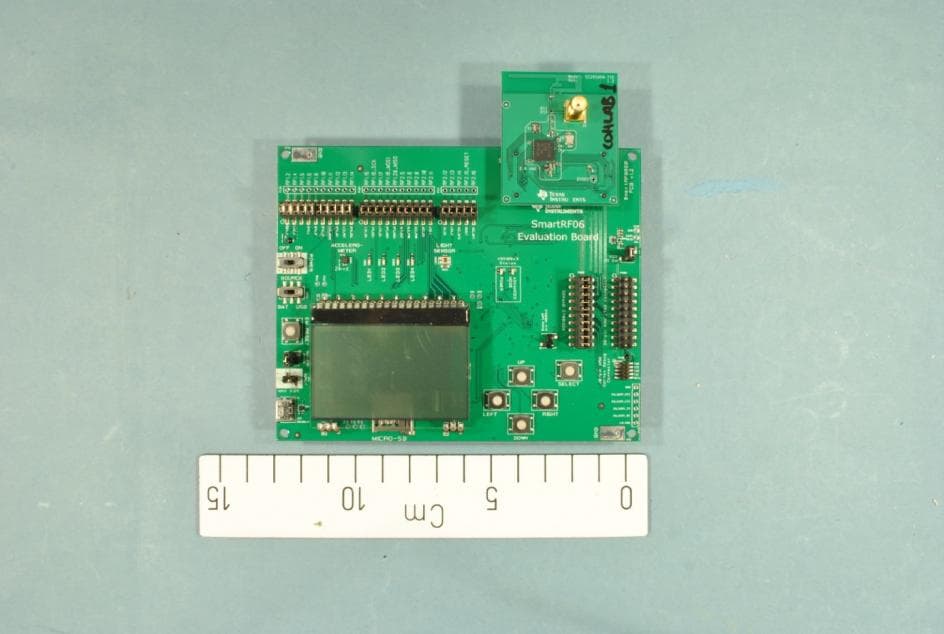
ZAT7IDEM
Feb 27, 2014The 7IDEM is a development tool for TIs 2.4 GHz 7ID System-on-Chip
Equipment Class
DTS - Digital Transmission System