ZAT85XX2590EMThe CC85xx-CC2590EM is a reference design for wireless audio modules including a range extender.
Texas Instruments Inc.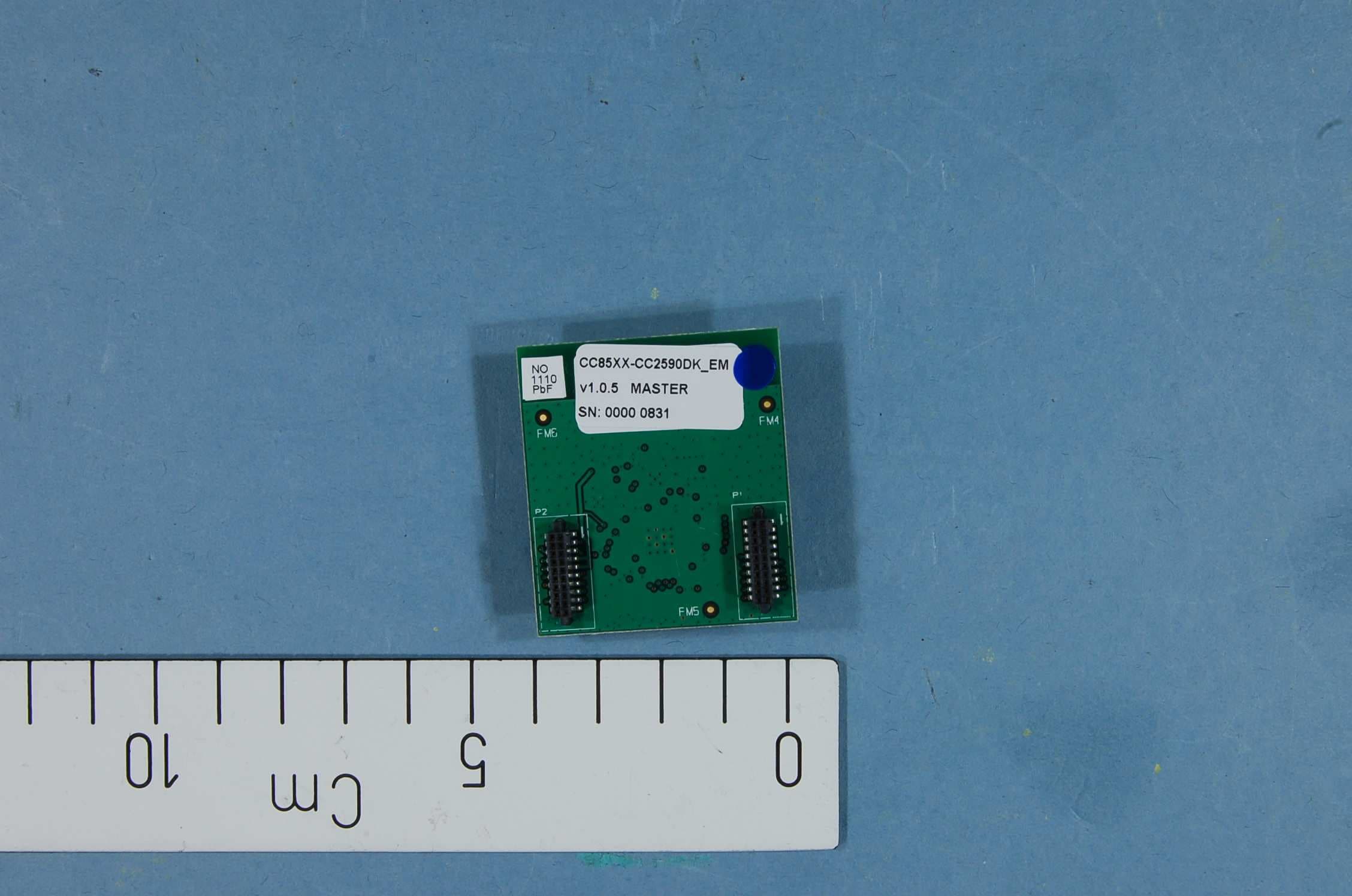
Click to zoom
Application Details
- Equipment Class
- DTS - Digital Transmission System
- Date of Grant
- Nov 06, 2012
- Application Purpose
- Original Equipment
- Date of Application
- Nov 05, 2012
- Equipment Note
- The CC85xx-CC2590EM is a reference design for wireless audio modules including a range extender.
- Frequency Range
- 2406.00000000 - 2474.00000000
- Company
- Texas Instruments Inc.
- Country
- United States
Documents & Files
Document Text
Text extracted from the exhibit documents filed with the FCC. Open a document above to read the original.
Users Manual
SWRU252B September 2012 CC85XXDK Quick Start Guide 1. Kit Contents The following items are included in the CC85XXDK: 2 x Purepath Wireless AudioEB 1 x CC Debugger 2 x CC85xxEM 2 x CC85xx-CC2590EM 2 x 2.4 GHz Antennas Cables Documentation The RF boards in this kit are FCC and IC certified and tested/comply with ETSI/R&TTE over temperature from 0 to +35°C. The antenna, W1010 from Pulse, is a ¼ wave dipole antenna with 2 dBi gain. 2. Purpose of this Quick Start Guide This quick start guide will provide step-by- step instructions showing how to set up an audio link between two wireless units provided in the development kit. The procedure is the same regardless of which evaluation module is being used, i.e. either the C85xxEM or the CC85xx- CC2590EM. The EMs are pre-programmed with firmware to stream audio from the (Master) line-in input of one AudioEB to the (Slave) line-out and headphone output on the other AudioEB. Please follow step 2 to 9. For the latest firmware revision see step 10. For more details on CC85xx, see the product folder of the CC8520 [1]. Caution! To minimize risk of injury, avoid touching components during operation if symbolized as hot. Caution! The kit contains ESD sensitive components. Handle with care to prevent permanent damage. 3. Plug Master EM into PPW Audio EB Connect the CC85xxEM or the CC85xx- CC2590EM marked MASTER (label attached on the backside of the board). These boards are pre-programmed with master firmware. Attach the antenna to the SMA connector. 4. Plug Slave EM into PPW Audio EB Connect the CC85xxEM or the CC85xx- CC2590EM marked SLAVE (label attached on the backside of the board.) These boards are pre-programmed with slave firmware. Attach the antenna to the SMA connector. 5. Connect Audio Cables to the Master Connect an audio source (CD-player, MP3-player or similar) to the line-in input of the AudioEB with CC85xxEM or CC85xx-CC2590 with the “MASTER” label plugged in. The CC85xx-CC2590EM and CC85xxEM with the “MASTER” label are pre- programmed with firmware which sets up the onboard TLV320AIC3101 codec [2] to use analog input on the PPW AudioEB. 6. Connect Audio Cables to the Slave Connect an amplifier to line out or connect a headphone to the mini jack of the AudioEB with the CC85xxEM or the CC85xx-CC2590 with the “SLAVE” label plugged in. The CC85xx-CC2590EM and CC85xxEM with the “SLAVE” label are pre- programmed with firmware which sets up the onboard TLV320AIC3101 codec [2] to use line out and headphone output of the PPW AudioEB. SWRU252B September 2012 7. Power To power the PPW AudioEBs; connect a USB cable to each of the PPW AudioEBs and make sure J10 is in the position “OUT-USB” (Pos 1-2). Finally, switch P6 to “ON”. The LED D3 should now be lit. Note! When using the DC jack connector or screw terminal to power the AudioEB, the power source should be in a range from 5.5V to 15V with a maximum current source capability of 1A. There should only be one active power source at any one time. Do not leave the board powered when unattended. 8. Pairing When powered for the first time, LED D9 will blink to indicate that the devices are not connected. To pair the Slave with the Master; click first on SW9 on Master and then click on SW9 on the Slave within a few seconds after you clicked on the Masters SW9. When the devices are paired and the link is established, LED D9 will be constantly lit. Note that the pairing operation is only needed the first time. Next time they will pair automatically when powered. You can now turn on your audio source and start testing! 9. Volume control The output volume can be adjusted on the Slave by pressing SW 1 to increase the volume and SW3 to decrease the volume. 10. PurePath Wireless Configurator The next step is to download the PurePath Wireless Configurator (PPWC). PPWC makes it possible to explore all the configuration options of the CC85xx family. After creating device configurations for Master and Slave network roles, PPWC can program the CC85xx devices directly through the CCDebugger (included in the kit). For more details; download the PPW Configurator and the PPW Configurator Quick Start Guide. Links to download the PPW Configurator can be found in the CC8520 product folder [1] A. More information On Texas Instruments’ Low-Power RF web site you will find information about our latest products, software, application notes, events and much more. Just go to www.ti.com/lprf The Low Power RF Online Community has forums, blogs and videos. Use the forums to find information, discuss and get help with your design. Join us at www.ti.com/lprf-forum The TI LPRF eNewsletter keeps you up to date on e.g. new products, application notes, software and events. Sign up at www.ti.com/lprfnewsletter We hope you will enjoy working with the CC8520 and associated Low-Power RF products from Texas Instruments. B. References [1] CC8520 product page www.ti.com/product/cc8520 [2] TLV320AIC3101 product page www.ti.com/product/tlv320aic3101 P6 J10 EVALUATION BOARD/KIT/MODULE (EVM) ADDITIONAL TERMS Texas Instruments (TI) provides the enclosed Evaluation Board/Kit/Module (EVM) under the following conditions: The user assumes all responsibility and liability for proper and safe handling of the goods. Further, the user indemnifies TI from all claims arising from the handling or use of the goods. Should this evaluation board/kit not meet the specifications indicated in the User’s Guide, the board/ kit may be returned within 30 days from the date of delivery for a full refund. THE FOREGOING LIMITED WARRANTY IS THE EXCLUSIVE WARRANTY MADE BY SELLER TO BUYER AND IS IN LIEU OF ALL OTHER WARRANTIES, EXPRESSED, IMPLIED, OR STATUTORY, INCLUDING ANY WARRANTY OF MERCHANTABILITY OR FITNESS FOR ANY PARTICULAR PURPOSE. EXCEPT TO THE EXTENT OF THE INDEMNITY SET FORTH ABOVE, NEITHER PARTY SHALL BE LIABLE TO THE OTHER FOR ANY INDIRECT, SPECIAL, INCIDENTAL, OR CONSEQUENTIAL DAMAGES. Please read the User's Guide and, specifically, the Warnings and Restrictions n…
Text truncated - open the document above for the full version.
Block Diagram
CC85xx-CC2590EM CC85xx f = <2400MHz – 2480MHz> CTRL LNA PA FREQUENCY SYNTHESIZER f_internal = <4800MHz – 4960MHz> f_output = <2400MHz – 2480MHz> AAF LPF ADC ADC DAC DAC DEMODULAT OR MODULATOR RADIO CONTROLLE R AND DATA INTERFACE QI QI RF_N RF_P I Q I Q CLOCK Gen X O S C _ Q 2 X O S C _ Q 1 Audio Clock Gen (135.4752 MHz) 48MHZ Crystal OSC ADC CLOCK CC2590 Audio interface MCLK=256x44.1 KHz BCLK=64x44.1kHz WCLK=44.1kHz
External Photos
FCC ID: ZAT85XX2590EM Project no.: 182244 Page 1 of 3 EXTERNAL PHOTOS – CC85XX-CC2590EM CC85XX-CC2590EM FCC ID: ZAT85XX2590EM Project no.: 182244 Page 2 of 3 PHOTOS OF ACCESSORIES Evaluation board – Front Evaluation board – rear FCC ID: ZAT85XX2590EM Project no.: 182244 Page 3 of 3 Whip antenna - Pulse W1010
ID Label/Location Info
Certification Document Label Description i/i Description of Labels for CC85XX-CC2590EM Labels Texas Instruments Model: CC85XX-CC2590EM (xxx) Rev. x.x.x S.No.: xxxxxx FCC ID: ZAT85XX2590EM IC: 451H-85XX2590EM ~ 1 3 m m ~ 25 mm ~ 6 m m ~ 9 mm The label is placed on the backside of the product. The illustration shows the label and product outline with approximate dimensions. ~ 4 5 m m ~ 40 mm Texas Instruments Model: CC85XX-CC2590EM (xxx) Rev. x.x.x S.No.: xxxxxx FCC ID: ZAT85XX2590EM IC: 451H-85XX2590EM Information about label and label material: Label manufacturer is Brady. Specific part info: Label part number B473 (http://www.bradyid.com/bradyid/domino/contentView.do/B473.html).
Internal Photos
FCC ID: ZAT85XX2590EM Project no.: 182244 Page 1 of 3 EXTERNAL PHOTOS – CC85XX-CC2590EM CC85XX-CC2590EM FCC ID: ZAT85XX2590EM Project no.: 182244 Page 2 of 3 PHOTOS OF ACCESSORIES Evaluation board – Front Evaluation board – rear FCC ID: ZAT85XX2590EM Project no.: 182244 Page 3 of 3 Whip antenna - Pulse W1010
Operational Description
Texas Instruments Norway AS Gaustadalléen 21 0349 Oslo Norway (+47) 22 95 85 44 (+47) 22 95 85 46 Technical Description The CC85xx-CC2590EM is an evaluation board for the CC85xx chip from Texas Instruments. The board will only function together with the PurePath Wireless Evaluation Board which is included in the CC85XXDK Development Kit. The CC85xx-CC2590EM is preloaded with an application image for audio streaming. In the CC85XXDK there are two CC85xx-CC2590EMs and one is programmed with a master image (audio producer), and the other is programmed with a slave image (audio consumer). The CC85xx System on Chip has a differential RF output. This differential output is connected to the differential RF input of the CC2590. The CC2590 has a single ended RF output which is low pass filtered with an external passive filter to reduce harmonic radiation. This filter is also transforming the signal to 50 ohm before it’s connected to an SMA connector. The antenna supplied with the board is W1010 from Pulse Electronics. The datasheet of the antenna is attached for further details.
Operational Description
W1010 Datasheet version 1.1 2/2008. Wireless External Antenna for 2.4 GHz Application © 2008. All Rights Reserved. Wireless External Antenna for 2.4 GHz Application Pulse Part Number: W1010 Pulse Finland Oy Takatie 6 90440 Kempele, Finland Tel: +358 207 935 500 Fax: +358 207 935 501 www.pulseeng.com/antennas Features - Shortest antennas in product line Omnidirectional radiation - For WLAN devices using WiFi (802.11b/g), Blu- etooth®, ZigBee™ and other applications in the ISM 2.4GHz band - Omnidirectional radiation pattern provides broad 360° coverage - One-quarter wavelength dipole configuration - Connection and color options easily integrate with OEM designs Connector - SMA (Male) Weight 6.3 grams Carton 20/bag; 500/carton Dimensions: Unless otherwise specified, all tolerances are ± Frequency [GHz] 2.4 – 2.5 Gain [dBi] 2.0 Impedance [Nom] 50 Ω VSWR ≤ 2.0 Polarization Vertical Radiation Omni Electrical Length ¼, dipole Electrical Specifications @ +25 °C Note: This part number is lead-free and RoHS compliant. No additional suffix or identifier is required. Inches mm 0.10 0.25 W1010 Datasheet version 1.1 2/2008. Wireless External Antenna for 2.4 GHz Application © 2008. All Rights Reserved. Wireless External Antenna for 2.4 GHz Application Pulse Part Number: W1010 Pulse Finland Oy Takatie 6 90440 Kempele, Finland Tel: +358 207 935 500 Fax: +358 207 935 501 www.pulseeng.com/antennas Application Notes Omni-directional antennas provide a uniform, donut- shaped, 360° radiation pattern. The omni-directional pat- tern is suitable for point-to-multipoint broadcasting in all directions. This antenna is primarily used for WLAN applications. However, it can also be used for a variety of other applications withing the spec ified frequency range. When used as an access point, the antenna is ideally located at the center of the coverage area. Gain Performance W1010 Vertical Position Horizontal Position
Parts List/Tune Up Info
CC85XX-CC2590EM R1.0.1 Assemble on CC85XX-CC2590EM R1.0 PCB Ref.Part namePcs/unitDescriptionManufacturerPart numberSupplierOrdering codeAlt. ManufacturerAlt. Part numberAlt. SupplierAlt. Ordering codeComments U2CC25901LNA and PA 10 dBmTICC2590TICC2590 U1CC85XX1PurePath W ireless transceiverTICC85XXTICC85XX C11;C13;C21;C103;C114C_04025Capacitor, general, 0402; Do not mount C101;C121;C181;C201;C231;C271;C311;C371C_100N_0402_X5R_K_108Capacitor, 100n, 0402, X5R, 10%, 10VMurataGRM155R71A104KA01D C131C_18P_0402_NP0_J_501Capacitor, 18p, 0402, NP0, 5% 25VMurataGRM1555C1H180JZ01DELFA65-881-23 C102;C132;C161C_1N_0402_NP0_J_503Capacitor, 1n, 0402, NP0, 5%, 50VMurataGRM1555C1H102JA01D C111C_1P2_0402_NP0_C_501Capacitor, 1p2, 0402, NP0, +/-0.25pF 50VMurataGRM1555C1H1R2CZ01D C113C_1P8_0402_NP0_C_501Capacitor, 1p8, 0402, NP0, +/-0.25pF 50VMurataGRM1555C1H1R8CZ01D C391;C401C_1U_0402_X5R_K_6P32Capacitor, 1u, 0402, X5R, 10%, 6.3VMurataGRM155R60J105KE19D C261C_220P_0402_NP0_J_501Capacitor, 220p, 0402, NP0, 5%, 50VMurataGRM1555C1H221JA01D C211;C221C_27P_0402_NP0_J_502Capacitor, 27p, 0402, NP0, 5%, 50VMurataGRM1555C1H270JZ01D C12;C104;C202C_2U2_0402_X5R_M_4VDC3Capacitor, 2u2, 0402, X5R, +/-20%, 4VMurataGRM1555C1H2R2CD01 C112C_6P8_0402_NP0_C_501Capacitor, 6p8, 0402, NP0, +-0.25pF 50VMurataGRM1555C1H6R8CZ01DELFA65-881-23 L112L_1N5_0402_S1Inductor, 1n5, 0402, Monolithic type, +/-0.3 nHMurataLQG15HS1N5S02DCoilcraft L111L_2N2_0402_B_LQW1Inductor, 2n2, 0402, +/-0.1nH, wire-wound typeMurataLQW 15AN2N2B00ACTE L113L_3N9_0402_B_LQW1#N/A#N/A#N/A#N/A#N/A#N/A#N/A#N/A#N/A#N/A L110;L131;L141;L151;L161;L291;L321;L331;L341;L351;L361L_6N8_0402_J11Inductor, 6n8, 0402, Monolithic type, ±5%MurataLQG15HS6N8J02D L11;L101;L202L_BEAD_102_04023EMI filter bead, 0402 1Kohms Tape GHz Band Gen UseMurataBLM15HG102SN1DACTE R71;R101;R241R_04023Resistor, general, 0402; Do not mount L171;L191;L381;R11;R21;R302R_0_04026Resistor, 0 ohm, 0402KoaRK73Z1ETTPELFA60-470-05 R1R_0_0402_3PORT_2-31Resistor 3 ports, 0 ohm, 0402, mounted between pad 2 and pad 3KoaRK73Z1ETTPELFA60-470-05 R291R_100K_0402_F1Resistor, 100k ohms, 0402, ±1% KoaRK73H1ETTP1003FELFA60-490-19 R361R_10K_0402_F1Resistor, 10k ohms, 0402, ±1% KoaRK73H1ETTP1002FELFA60-485-32 R72;R151R_4K3_0402_G2Resistor, 4k3 ohms, 0402, 2%KoaRK73H1ETTP4301FELFA60-483-59 R301R_56K_0402_F1Resistor, 56k ohms, 0402, ±1% KoaRK73H1ETTP5602FELFA60-488-96 P3SMA_SMD1SMA connector, straight SMD-mountHus-Tsan Group TaiwanSMA-10V21-TGGEC Partner A/SSMA-10V21-TGGAFU, Arrow P1-2SMD_SOCKET_2X102SMD pinrow socket, .050 spacing, 2x10SamtecSFM-110-02-SM-D-A-K-TRAbacusAFU, Arrow X1X_48.000/15/18/60/161Crystal, 48.000000MHz, 16.0pF, +/-15ppm (FT), +/-18ppm (FS), 60 ohms max. Epson ToyocomFA-128 48.000000MHz, Q22FA12800044EpsonQ22FA12800044 Total number of components66
Schematics
GIO3 GIO1 GIO2 USBM USBP GIO1 GIO2 MCLK WCLK MISO MISO CSN CSN MOSI MOSI SCLK SCLK BCLK MCLKAD1WCLKAD0BCLK SCL SDA SCLSDA GIO13 GIO12 GIO3 USBP USBM AD1 AD0 AD2 AD2 GIO13GIO12 AVDD_CC2590 AVDD_CC2590 VDD IOVDD VDD VDD 3V3 VDD VDD 1V8 IOVDD 1V8 IOVDD IOVDD 3V3 3V3 3V3 IOVDD VDD 1 2 C132 C_1N_0402_NP0_J_50 1 2 3 4 5 P3 SMA_SMD 1 2 3 4 5 6 7 8 9 10 11 12 13 14 15 16 17 AVDD_PA GND ANT GND AVDD_LNA RF_N RXTX RF_P PAEN EN HGM GND AVDD_BIAS GND PABIAS GND UNUSED U2 CC2590 1 2 C102 C_1N_0402_NP0_J_50 1 2 3 4 5 6 7 8 9 10 11121314151617181920 21 22 23 24 25 26 27 28 29 30 3132333435363738394041 XI XO AVDD VBAT DVDDDCPLGIO15 RBIAS AVDD RF_P AVDD AVDD SCLSDA GIO12GIO13GIO14 GND_EXPOSED USBM USBP CSN SCLK MOSI MISO GIO1 GIO2 GIO3 RF_N RSTNMCLKBCLKWCLKAD0AD1AD2AVDD AVDD IOVDD IOVDDIOVDD XI XO IOVDD U1 CC85XX 1 2 3 4 GND X1 X_48.000/15/18/60/16 1 2 C161 C_1N_0402_NP0_J_50 12 R302 R_0_0402 1 2 3 A1 Antenna_IIFA_cc2420 1 2 C121 C_100N_0402_X5R_K_10 1 2 C201 C_100N_0402_X5R_K_10 1 2 C391 C_1U_0402_X5R_K_6P3 1 2 C271 C_100N_0402_X5R_K_10 1 2 C103 C_0402 1 2 C114 C_0402 1 2 C181 C_100N_0402_X5R_K_10 1 2 C371 C_100N_0402_X5R_K_10 1 2 C202 C_2U2_0402_X5R_M_4VDC 1 2 C101 C_100N_0402_X5R_K_10 1 2 C231 C_100N_0402_X5R_K_10 1 2 C221 C_27P_0402_NP0_J_50 1 2 C211 C_27P_0402_NP0_J_50 1 2 C401 C_1U_0402_X5R_K_6P3 1 2 C104 C_2U2_0402_X5R_M_4VDC 1 2 C13 C_0402 1 2 C12 C_2U2_0402_X5R_M_4VDC 1 2 C21 C_0402 1 2 C261 C_220P_0402_NP0_J_50 1 2 C112 C_6P8_0402_NP0_C_50 1 2 C111 C_1P2_0402_NP0_C_50 12 C113 C_1P8_0402_NP0_C_50 1 2 C311 C_100N_0402_X5R_K_10 1 2 C11 C_0402 1 2 C131 C_18P_0402_NP0_J_50 1 FM1 FIDUCIAL_MARK_1MM 1 FM3 FIDUCIAL_MARK_1MM 1 FM2 FIDUCIAL_MARK_1MM 1 FM4 FIDUCIAL_MARK_1MM 1 FM5 FIDUCIAL_MARK_1MM 1 FM6 FIDUCIAL_MARK_1MM 12 L112 L_1N5_0402_S 1 2 L113L_3N9_0402_B_LQW 1 2 L111 L_2N2_0402_B_LQW 12 L101 L_BEAD_102_0402 12 L202 L_BEAD_102_0402 12 L11 L_BEAD_102_0402 1 2 L341 L_6N8_0402_J 1 2 L131 L_6N8_0402_J 1 2 L351 L_6N8_0402_J 1 2 L141 L_6N8_0402_J 1 2 L361 L_6N8_0402_J 1 2 L151 L_6N8_0402_J 1 2 L161 L_6N8_0402_J 1 2 L291 L_6N8_0402_J 1 2 L331 L_6N8_0402_J 1 2 L321 L_6N8_0402_J 1 2 L110 L_6N8_0402_J 1 2 R301 R_56K_0402_F 12 R21 R_0_0402 1 2 L191 R_0_0402 12 R11 R_0_0402 1 2 L171 R_0_0402 1 2 L381 R_0_0402 1 2 R72 R_4K3_0402_G 1 2 R241 R_0402 12 R101 R_0402 1 2 R71 R_0402 12 R151 R_4K3_0402_G 1 2 R361 R_10K_0402_F 1 2 VBAT R291 R_100K_0402_F 1 2 3 R1R_0_0402_3PORT_2-3 12 34 56 78 910 1112 1314 1516 17 18 1920 RSTN P2 SMD_SOCKET_2X10 1 2 34 56 78 910 1112 1314 1516 1718 1920 P1 SMD_SOCKET_2X10 A3 SCALESHEET APPROVALS DATE REV.DWG NO. DWG COMPANY NAME ISSUED CHECKED DRAWN FSCM NO.SIZE CONTRACT NO. Texas Instruments 1 of 1 TLIN inductor TLIN inductor CC85XX-CC2590EM Use only for CC2591. C13 1000pF TSK 1.0.1 TLIN inductor TLIN inductor 03233
Test Report
Nemko AS, Gaustadalléen 30, P.O.Box 73 Blindern, NO-0314 Oslo Norway T +47 22 96 03 30 F +47 22 96 05 50 Enterprise number NO974404532 Visiting address: Nemko Kjeller, Instituttveien 6, P.O.Box 96, NO-2027 Kjeller Norway T +47 64 84 57 00 F +47 64 84 57 05 Test report no. : 182244-3 Item tested : CC85xx-CC2590EM Type of equipment : 2.4GHz wireless audio transceiver FCC ID : ZAT85XXCC2590EM IC ID: 451H-85XX2590EM Client : Texas Instruments Norway AS FCC Part 15.247 Digital Transmission System RSS-210, Issue 8 Low Power Licence-Exempt Radiocommunication Devices 2012-10-16 Authorized by : .............................................. Frode Sveiensen Technical Verificator TEST REPORT FCC part 15.247 Ref. no.: 182244-3 FCC ID: ZAT85XX2590EM & IC-ID:451H-85XX2590EM Nemko AS, NO-2027 Kjeller Page 2 (38) CONTENTS 1 GENERAL INFORMATION ...................................................................................................... 3 1.1 Testhouse Info .......................................................................................................................... 3 1.2 Client Information ...................................................................................................................... 3 1.3 Responsible Manufacturer (If other than client) ........................................................................ 3 2 Test Information ...................................................................................................................... 4 2.1 Test Item ................................................................................................................................... 4 2.2 Test Environment ...................................................................................................................... 5 2.2.1 Normal test condition ................................................................................................... 5 2.3 Test Period................................................................................................................................ 5 3 TEST REPORT SUMMARY ..................................................................................................... 6 3.1 General ..................................................................................................................................... 6 3.2 Test Summary ........................................................................................................................... 7 3.3 Description of modification for Modification Filing ..................................................................... 7 3.4 Comments ................................................................................................................................ 7 3.5 Family List Rational .................................................................................................................. 7 3.6 Test Engineer(s) ....................................................................................................................... 7 4 TEST RESULTS ....................................................................................................................... 8 4.1 Minimum 6 dB Bandwidth ......................................................................................................... 8 4.2 20 dB Bandwidth ..................................................................................................................... 10 4.3 Peak Power Output ................................................................................................................. 11 4.4 Spurious Emissions (Radiated) .............................................................................................. 18 4.5 Receiver Spurious Emissions ................................................................................................. 30 4.6 Power Spectral Density (PSD) ................................................................................................ 35 5 LIST OF TEST EQUIPMENT .................................................................................................. 37 6 BLOCK DIAGRAM ................................................................................................................. 38 6.1 Power Line Conducted Emission ............................................................................................ 38 6.2 Test Site Radiated Emission ................................................................................................... 38 TEST REPORT FCC part 15.247 Ref. no.: 182244-3 FCC ID: ZAT85XX2590EM & IC-ID:451H-85XX2590EM Nemko AS, NO-2027 Kjeller Page 3 (38) 1 GENERAL INFORMATION 1.1 Testhouse Info Name : Nemko AS Address : Nemko Kjeller Instituttveien 6, Box 96 NO-2027 Kjeller, NORWAY Telephone : +47 64 84 57 00 Fax : +47 64 84 57 05 E-mail: [email protected] FCC test firm : 994405 IC OATS : 2040D-1 Total Number of Pages: 38 1.2 Client Information Name : Texas Instruments Norway AS Address : Gaustadalléen 21, NO-0349 Oslo, Norway Telephone : +47 22 95 85 44 Fax : +47 22 95 85 46 Contact: Name : Fredrik Kervel Telephone : +47 22 95 83 62 E-mail : [email protected] 1.3 Responsible Manufacturer (If other than client) Name : / Address : / TEST REPORT FCC part 15.247 Ref. no.: 182244-3 FCC ID: ZAT85XX2590EM & IC-ID:451H-85XX2590EM Nemko AS, NO-2027 Kjeller Page 4 (38) 2 Test Information 2.1 Test Item Name : Texas Instruments Model/version : CC85XX-CC2590EM Serial number : - Hardware identity and/or version: - Software identity and/or version : - Frequency Range : 2406 – 2474 MHz Number of Channels : 4 (out of 18) Channel BW: >2MHz Channel spacing: 4MHz Operating Modes : Transceiver Type of Modulation : Shaped 8GFSK, (DSSS) Data rate: 5000kbit/s User Frequency Adjustment : None, Software controlled Conducted Output Power : 0.0067 Watts (Peak) Type of Power Supply : Battery 9.0Vdc Antenna Connector : SMA Antenna type: Whip antenna - Pulse W1010 Antenna Diversity Supported : None Theory of Operat…
Text truncated - open the document above for the full version.
Test Setup Photos
FCC ID: ZAT85XXCC2590EM Project no.: 182244 Page 1 of 1 PHOTOS OF TEST SET-UP – CC85XX-CC2590EM Radiated Emissions
Contact Information
Applicant
Marian Kost(Product Line Manager, Connectivity)
Technical Contact
Texas instruments Norway ASKristoffer Starheim
[email protected]+4722958319
Gaustadalleen 21 · Oslo · Norway
Non-Technical Contact
Nemko USA, Inc.Zarah G MacIvor
[email protected]214-629-5683
Test Firm
Nemko ASFrode Sveinsen
Technical Specifications
| # | Rule Parts | Frequency Range | Power Output |
|---|---|---|---|
| 1 | 15C | 2.41 GHz - 2.47 GHz | 6.70 mW |
Other Applications from Texas Instruments Inc.
ZAT-2340R5MODA
Jan 30, 2026CC2340R5MODAN0MHAR
Equipment Class
DTS - Digital Transmission SystemZAT-1312PSIP-3
May 19, 2024CC1312PSIP
Equipment Class
DSS - Part 15 Spread Spectrum TransmitterZAT-1312PSIP-2
Jan 21, 2024CC1312PSIP
Equipment Class
DSS - Part 15 Spread Spectrum Transmitter
ZAT-1312PSIP-1
Jul 09, 2023CC1312PSIP
Equipment Class
DSS - Part 15 Spread Spectrum Transmitter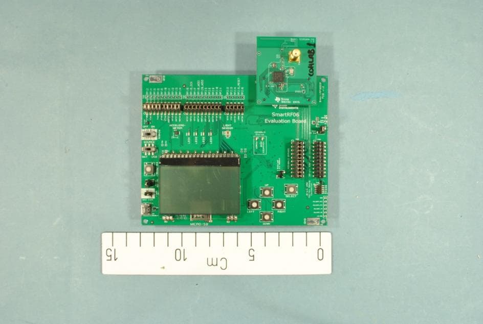
ZAT7IDEM
Feb 27, 2014The 7IDEM is a development tool for TIs 2.4 GHz 7ID System-on-Chip
Equipment Class
DTS - Digital Transmission System