ZAT85XXHEADSETThe CC85xxHeadset is a reference design for wireless audio headsets for development only and cannot be used in an end product.
Texas Instruments Inc.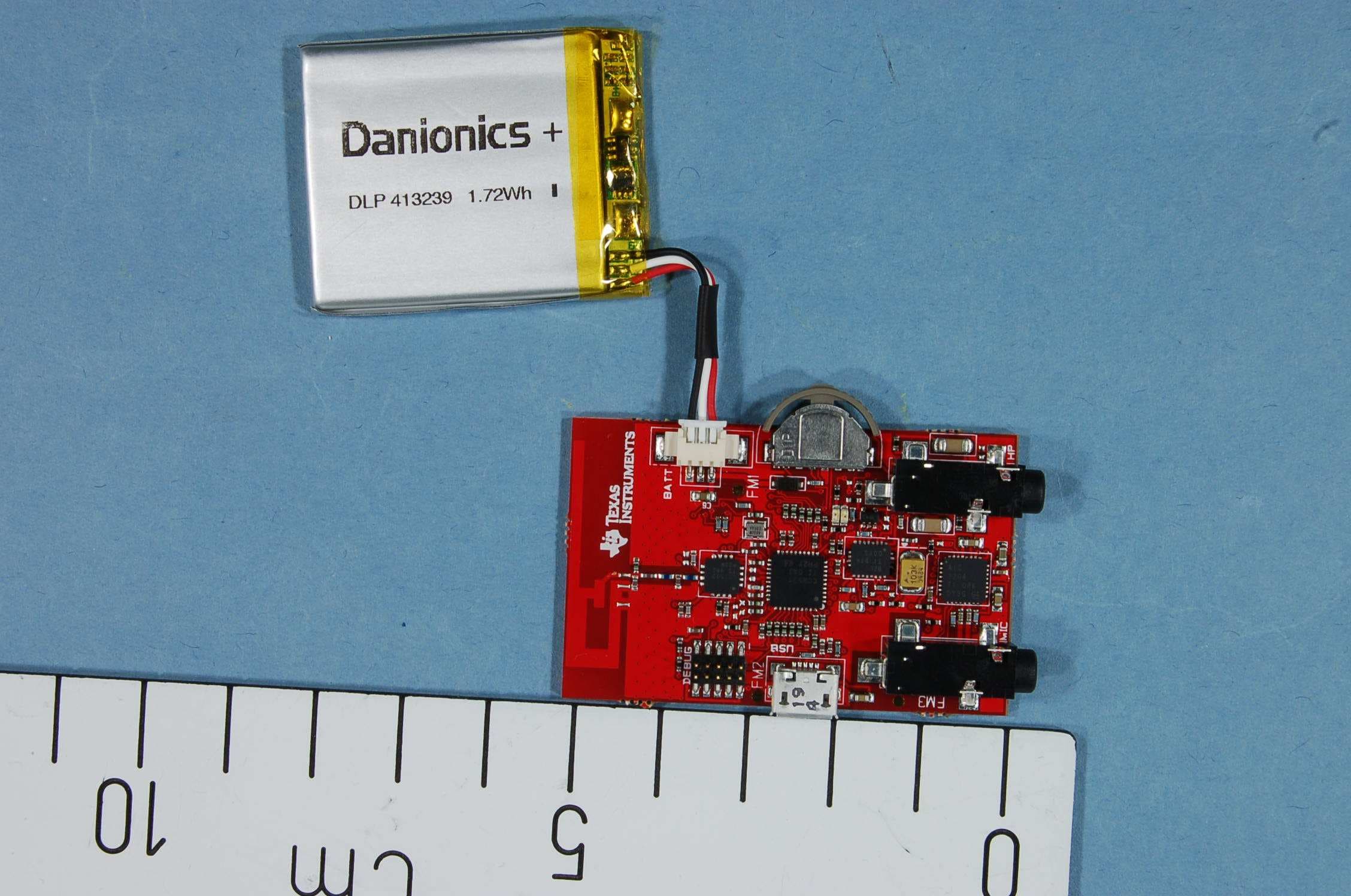
Click to zoom
Application Details
- Equipment Class
- DTS - Digital Transmission System
- Date of Grant
- Sep 25, 2012
- Application Purpose
- Original Equipment
- Date of Application
- Sep 25, 2012
- Equipment Note
- The CC85xxHeadset is a reference design for wireless audio headsets for development only and cannot be used in an end product.
- Frequency Range
- 2406.50000000 - 2474.50000000
- Company
- Texas Instruments Inc.
- Country
- United States
Documents & Files
Document Text
Text extracted from the exhibit documents filed with the FCC. Open a document above to read the original.
Users Manual
SWRU282A June 2012 CC85XXDK-HEADSET Quick Start Guide 1. Kit Contents The following items are included in the CC85XXDK-HEADSET: 2 x CC85XX Headset boards 2 x Battery 1 x CC Debugger 1 x USB micro cable 1 x 3.5mm jack to 3.5mm jack cable Documentation If anything is missing in the CC85XXDK- HEADSET please contact your local TI sales representative. Caution! The kit contains ESD sensitive components. Handle with care to prevent permanent damage. 2. Purpose of this Quick Start Guide This quick start guide will provide step-by- step instructions showing how to set up an audio link between two wireless units provided in the development kit. The CC8531 on each of the boards are pre-programmed with firmware to stream audio from the Master microphone input to the Slave headphone output. Please follow step 3 to 9. Information on how to upgrade with latest firmware, see step 10. For more details on CC85XX, see the product folder of the CC8520 [1]. Performance and functionality of the CC8531 are strongly dependant on the firmware. Thus, for performance testing etc make sure the firmware used is the latest released firmware from the TI web site, see step 10. 3. Plug the batteries to each of the Headset boards There’s only one way to connect the battery plug to the socket on the board. With the pre-programmed firmware the CC8531 enters the OFF power mode when the battery is connected. The batteries should have enough charge out- of-the-box to establish a link and stream audio. To charge the battery, see section 9. With full battery the link should run for typically 15 hours, the Master being the bottleneck. The Slave plays audio for 22 hours typically. Warning! Always use the battery supplied with the kits with the CC85xx Headset boards. 4. Power up both boards In the pre-programmed firmware the toggling between power modes OFF and ON is mapped to pressing the rocker switch IN for 1.6 seconds. The two boards are unpaired out-of-the-box, so in the ON power mode the topmost LED should flash once every second indicating network state ALONE . In the OFF power mode the LED is turned off. Make sure both boards are flashing. Caution! To minimize risk of injury, avoid touching components during operation if symbolized as hot. Do not leave EVM powered when unattended. 5. Connect an audio source to the Master Connect an audio source (CD-player, MP3-player or similar) to the line in connector on the Master Headset board (labeled Master on the back side) via the 3.5mm jack cable. The Master is pre-programmed with firmware to set up the onboard TLV320AIC3204 codec [2] to power down the DAC and use the line in connector as source to the ADC input. 6. Connect a headphone to the Slave Connect a headphone to the 3.5mm headphone output on the board labeled Slave on the back side. The Slave is pre-programmed with firmware to set up the onboard TLV320AIC3204 codec [2] to power down the ADC and have the headphone connector as destination of the DAC output. SWRU282A June 2012 7. Pairing In the pre-programmed firmware the pairing button is mapped to pressing the rocker switch IN (not hold, which is power toggling as described in 4). Press the pairing button on either board and observe that the LED blinking pattern changes. It will now flash two times per second which indicates that the device is trying to pair with another device. If the pairing button on the other board is pressed within 10 seconds the devices will pair. The Master status LED will be constantly lit, and the Slave status LED will flash once every 2.5 seconds. Audio is now being streamed to the Slave. When successfully paired the Slave will save the Master’s device ID in non-volatile memory and automatically try to pair with this Master whenever in the ALONE state. Thus pressing the pairing buttons again will no longer be necessary (unless the Slave is re-programmed or paired with another Master). 8. Volume control The pre-programmed Slave firmware is configured to have so-called “local volume control” meaning that the Slave controls its own volume locally. The volume buttons are mapped to clicking/holding the rocker switch UP and DOWN. 9. Charging To charge the battery, simply connect the USB micro cable while the battery is also connected. The charge voltage should be 5V (plugging the USB cable in your computer will work perfectly). The bottom LED will be lit indicating charging. When the battery is fully charged the LED will go dark. The Headset board can be powered from USB alone (remove the battery and connect USB cable). Then the LED will be lit the whole time. Audio can be streamed while charging. For information about the single chip charger and DC/DC converter, see [4]. 10. PurePath Wireless Configurator The next step is to download the PurePath Wireless Configurator (PPWC) [3]. PPWC makes it possible to explore all the configuration options of the CC85XX family. After creating device configurations for Master and Slave network roles, PPWC can program the CC85XX devices directly through the CCDebugger (included in the kit). A. More information On Texas Instruments’ Low-Power RF web site you will find all our latest products, application and design notes, FAQ section, news and events updates, and much more. Just go to www.ti.com/lprf The Low Power RF Online Community has forums, blogs and videos. Use the forums to find information, discuss and get help with your design. Join us at www.ti.com/lprf-forum The TI LPRF eNewsletter keeps you up to date on e.g. new products, application notes, software and events. Sign up at www.ti.com/lprfnewsletter We hope you will enjoy working with the CC85XX and associated Low-Power RF products from Texas Instruments. B. References [1] CC8520 product web page http://www.ti.com/CC8520 [2] TLV320AIC3204 product web page http://focus.ti.com/docs/prod/folders/p rint/tlv320aic3204.html [3] PPW Configurator product web page http://www.ti.com/ppwc [4] BQ25015 product web page http://focus.ti.com/docs/prod/folders/p rint/bq25…
Text truncated - open the document above for the full version.
Block Diagram
CC85xxHEADSET CC85xx f = <2400MHz – 2480MHz> CTRL LNA PA FREQUENCY SYNTHESIZER f_internal = <4800MHz – 4960MHz> f_output = <2400MHz – 2480MHz> AAF LPF ADC ADC DAC DAC DEMODULAT OR MODULATOR RADIO CONTROLLE R AND DATA INTERFACE QI QI RF_N RF_P I Q I Q CLOCK Gen X O S C _ Q 2 X O S C _ Q 1 Audio Clock Gen (135.4752 MHz) 48MHZ Crystal OSC ADC CLOCK CC2590 Audio Codec (TLV320AIC3204) Audio interface MCLK=256x44.1 KHz BCLK=64x44.1kHz WCLK=44.1kHz
External Photos
FCC ID: / Project no.: 182240 Page 1 of 1 EXTERNAL PHOTOS – CC85xx Headset
ID Label/Location Info
Certification Document Label Description i/i Description of Labels for CC85XXHEADSET Labels Texas Instruments Model: CC85XXHEADSET (xxx) Rev. x.x.x S.No.: xxxxxx FCC ID: ZAT85XXHEADSET IC: 451H-85XXHEADSET ~ 1 3 m m ~ 25 mm ~ 6 m m ~ 9 mm The label is placed on the backside of the product. The illustration shows the label and product outline with approximate dimensions. T e x a s I n s t r u m e n t s M o d e l : C C 8 5 X X H E A D S E T ( x x x ) R e v . x . x . x S . N o . : x x x x x x F C C I D : Z A T 8 5 X X H E A D S E T I C : 4 5 1 H - 8 5 X X H E A D S E T ~ 5 1 m m ~ 33 mm
Internal Photos
FCC ID: / Project no.: 182240 Page 1 of 1 INTERNAL PHOTOS – CC85xx Headset
Operational Description
Texas Instruments Norway AS Gaustadalléen 21 0349 Oslo Norway (+47) 22 95 85 44 (+47) 22 95 85 46 Technical Description The CC85xxHeadset, see Figure 1, based on the Texas Instruments’ CC8531, is SoC for streaming wireless audio, the CC85xxHeadset also includes the CC2590 which is a integrated Power amplifier and Low Noise amplifier. The CC85xxHeadset is pre- programmed and the output power level is fixed Figure 1 CC85xxHeadset Texas Instruments Norway AS Gaustadalléen 21 0349 Oslo Norway (+47) 22 95 85 44 (+47) 22 95 85 46 Antenna description The CC85xxHeadset has an integrated inverted-F PCB antenna, see Figure 2. The typical output power of the CC8531 together with the CC2590 device is 11 dBm on 2440 MHz, the insertion loss in the balun, is typically 0.6 dB and the maximum e.i.r.p. was measured to be 16 dBm, i.e. the maximum antenna gain would be: Maximum e.i.r.p.: 16 dBm Insertion loss: 0.6 dB Conducted output power: 11 dBm Maximum antenna gain: 4.4 dB Figure 2 CC85xxHeadset PCB antenna
RF Exposure Info
Prediction of MPE limit at a given distance M W-CBDA-SMR-10W80-PS8, Uplink Outdoor Donar Antenna Equation from page 18 of OET Bulletin 65, Edition 97-01where: S = power density P = power input to the antennaG = power gain of the antenna in the direction of interest relative to an isotropic radiatorR = distance to the center of radiation of the antenna Maximum peak output power at antenna input terminal: 13.10 (dBm) Maximum peak output power at antenna input terminal: 20.41737945 (mW) Antenna gain(typical): 3.5 (dBi) Maximum antenna gain: 2.238721139 (numeric) Prediction distance: 20 (cm) Prediction frequency: 2400 (MHz) MPE limit for uncontrolled exposure at prediction frequency: 1 (mW/cm^2) Power density at prediction frequency: 0.009093 (mW/cm^2) Maximum allowable antenna gain: 23.91269855 (dBi) Margin of Compliance: 20.41269855 2 4 R PG S π =
Test Report
Nemko AS, Gaustadalléen 30, P.O.Box 73 Blindern, NO-0314 Oslo Norway T +47 22 96 03 30 F +47 22 96 05 50 Enterprise number NO974404532 Visiting address: Nemko Kjeller, Instituttveien 6, P.O.Box 96, NO-2027 Kjeller Norway T +47 64 84 57 00 F +47 64 84 57 05 Test report no. : 182240-5 Item tested : CC85xxHEADSET Type of equipment : 2.4GHz Transceiver FCC ID : ZAT85XXHEADSET Client : Texas Instruments Norway AS FCC Part 15.247 Digital Transmission System RSS-210, Issue 8 Low Power Licence-Exempt Radiocommunication Devices 2012-09-27 Authorized by : .............................................. Geir Antonsen Technical Verificator TEST REPORT FCC part 15.247 Ref. no.: 182240-5 FCC ID: ZAT85XXHEADSET Nemko AS, NO-2027 Kjeller Page 2 (33) CONTENTS 1 GENERAL INFORMATION ...................................................................................................... 3 1.1 Testhouse Info .......................................................................................................................... 3 1.2 Client Information ...................................................................................................................... 3 1.3 Responsible Manufacturer (If other than client) ........................................................................ 3 2 Test Information ...................................................................................................................... 4 2.1 Test Item ................................................................................................................................... 4 2.2 Test Environment ...................................................................................................................... 5 2.3 Test Period................................................................................................................................ 5 3 TEST REPORT SUMMARY ..................................................................................................... 6 3.1 General ..................................................................................................................................... 6 3.2 Test Summary ........................................................................................................................... 7 3.3 Description of modification for Modification Filing ..................................................................... 7 3.4 Comments ................................................................................................................................ 7 3.5 Family List Rational .................................................................................................................. 7 4 TEST RESULTS ....................................................................................................................... 8 4.1 Minimum 6 dB Bandwidth ......................................................................................................... 8 4.2 20 dB Bandwidth ....................................................................................................................... 9 4.3 Peak Power Output ................................................................................................................. 10 4.4 Spurious Emissions (Radiated) .............................................................................................. 13 4.5 Receiver Spurious Emissions ................................................................................................. 29 4.6 Power Spectral Density (PSD) ................................................................................................ 30 5 LIST OF TEST EQUIPMENT .................................................................................................. 32 6 BLOCK DIAGRAM ................................................................................................................. 33 6.1 Test Site Radiated Emission ................................................................................................... 33 TEST REPORT FCC part 15.247 Ref. no.: 182240-5 FCC ID: ZAT85XXHEADSET Nemko AS, NO-2027 Kjeller Page 3 (33) 1 GENERAL INFORMATION 1.1 Testhouse Info Name : Nemko AS Address : Nemko Kjeller Instituttveien 6, Box 96 NO-2027 Kjeller, NORWAY Telephone : +47 64 84 57 00 Fax : +47 64 84 57 05 E-mail: [email protected] FCC test firm : 994405 IC OATS : 2040D-1 Total Number of Pages: 33 1.2 Client Information Name : Texas Instruments Norway AS Address : Gaustadalléen 21, NO-0349 Oslo, Norway Telephone : +47 22 95 85 44 Fax : +47 22 95 85 46 Contact: Name : Fredrik Kervel Telephone : +47 22 95 8362 E-mail : [email protected] 1.3 Responsible Manufacturer (If other than client) Same as client. TEST REPORT FCC part 15.247 Ref. no.: 182240-5 FCC ID: ZAT85XXHEADSET Nemko AS, NO-2027 Kjeller Page 4 (33) 2 Test Information 2.1 Test Item Name : Texas Instruments FCC ID : ZAT85XXHEADSET Model/version : CC85xxHEADSET Serial number : / Hardware identity and/or version: / Software identity and/or version : / Frequency Range : 2406.5 – 2474.5 MHz Number of Channels : 18 Output Power : 20.4 mW (calculated conducted) Type of Modulation : Digital User Frequency Adjustment : None Type of Power Supply : Powered from Secondary Battery (3.7V Li-Ion) Antenna Connector : None (Integral Antenna) Antenna Diversity Supported : No Desktop Charger : None Description of Test Item The tested EUT is a 2.4GHz wireless audio transceiver. TEST REPORT FCC part 15.247 Ref. no.: 182240-5 FCC ID: ZAT85XXHEADSET Nemko AS, NO-2027 Kjeller Page 5 (33) 2.2 Test Environment 2.2.1 Normal test condition Temperature: 20 - 22 °C Relative humidity: 42 - 52 % Normal test voltage: 3.7 V DC The radiated tests were performed with the EUT powered from fully charged batteries. The values are the limit registered during the test period. 2.3 Test Period Item received date: 2011-08-15 Test period : from 2011-08-12 to 2011-08-22 TEST REPORT FCC part 15.247 Ref. no.: 182240-5 FCC ID: ZAT85…
Text truncated - open the document above for the full version.
Test Setup Photos
FCC ID: / Project no.: 182240 Page 1 of 2 PHOTOS OF TEST SET-UP – CC85xx Headset Radiated Emissions 30 - 1000 MHz Radiated Emissions 1 - 12 GHz FCC ID: / Project no.: 182240 Page 2 of 2 Power line Conducted Emissions Test
Contact Information
Applicant
Marian Kost(Product Line Manager, Connectivity)
Technical Contact
Texas instruments Norway ASP�r Haakansson
[email protected]004722958544
Gaustadall�en 21 · Oslo · Norway
Test Firm
Nemko ASFrode Sveinsen
Technical Specifications
| # | Rule Parts | Frequency Range | Power Output |
|---|---|---|---|
| 1 | 15C | 2.41 GHz - 2.47 GHz | 20.40 mW |
Other Applications from Texas Instruments Inc.
ZAT-2340R5MODA
Jan 30, 2026CC2340R5MODAN0MHAR
Equipment Class
DTS - Digital Transmission SystemZAT-1312PSIP-3
May 19, 2024CC1312PSIP
Equipment Class
DSS - Part 15 Spread Spectrum TransmitterZAT-1312PSIP-2
Jan 21, 2024CC1312PSIP
Equipment Class
DSS - Part 15 Spread Spectrum Transmitter
ZAT-1312PSIP-1
Jul 09, 2023CC1312PSIP
Equipment Class
DSS - Part 15 Spread Spectrum Transmitter
ZAT7IDEM
Feb 27, 2014The 7IDEM is a development tool for TIs 2.4 GHz 7ID System-on-Chip
Equipment Class
DTS - Digital Transmission System