2AALG-NWP-F110Neo smartpen N2
NEOLAB CONVERGENCE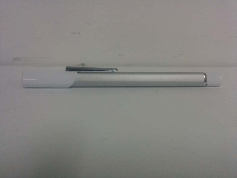
Click to zoom
Application Details
- Equipment Class
- DTS - Digital Transmission System
- Date of Grant
- Sep 18, 2014
- Application Purpose
- Original Equipment
- Date of Application
- Sep 18, 2014
- Equipment Note
- Neo smartpen N2
- Frequency Range
- 2402.00000000 - 2480.00000000
- Company
- NEOLAB CONVERGENCE
- Country
- South Korea
Documents & Files
Document Text
Text extracted from the exhibit documents filed with the FCC. Open a document above to read the original.
Users Manual
User Guide 3. Product Package +40° -20° +40° -20° Neo smartpen N2 Refill pen tip 1 EA User Manual (Product warranty) Micro USB Cable (For charging and data transfer) Getting Started Before using the product, please read the instructions. In order to increase the product’s performance and usability, updates could occur without any notice. 1. The current product supports Android 4.2 or higher and iOS iPhone 5 or higher. 2. Please check if your smart device supports Bluetooth. The product cannot be used without the Bluetooth function. 3. If the product is disassembled by an unauthorized individual (or user), it could cause damage and the warranty services will not be provided. 4. Please be careful not to drop the product or cause external impact, especially the pen’s recognition sensor at the bottom part. 5. Please avoid places or materials that has high static electricity. 6. The warranty will be void if the product has been damaged by immersion in water. 7. When fully charged, please distich the product from the AC/DC adapter. 8. Overcharging or over discharge by not using the product for long periods can cause damage to the battery. 9. Chemical or any related cleanser could cause alteration of the product. 10. Please avoid dusty and humid places. Also, avoid magnetic, and direct sunlight. 11. Please place the product out of reach from children. If the children put the product in their mouth, serious injury could occur. 12. After reading the instructions, place the instruction where it could be easily found. 5. N-note (Neo smartpen 2’s exclusive note)Preparing for application 1. Application (App) for Neo smartpen N2 can be downloaded from Android ‘Google Play’ store or iOS ‘App Store’. Type and search for “Neo smartpen N2”! 2. You can download, install, and update from ‘Google Play’ store or ‘App Store’ 3. In order to use the App, Neo smartpen N2 needs to be connected via Bluetooth. 4. When connected properly, the content from the N-note will appear to the screen. You can download the Neo smartpen N2 application from ‘Google Play Store’ or ‘iOS App Store’ Supporting OS Supported device Android 4.2 or higher / iOS iPhone 5 or higher Bluetooth 2.0 or higher supporting device Neo smartpen N2 and its App can be used only with N-note and smart diary Find N-notes in Neo smartpen n2 stores! More N-note designs will be developed and launched. 2014 Smart Diary SETN note Basic 01/02/03N note Premium L/M/SN note Snowcat L/M/S Cautions in use of N-note If you use a new note of the same kind, the written contents of the new note can be overlap the existing one. In this case, you can use the new note after saving the existing note by using the function, [Store existing note]. * In order to learn [Store existing note], please see the pages 13p of the manual. 7. Neo smartpen N2 Basic Operating MethodNeo smartpen N2 Product Image Side Pen tip (replaceable) Power button Camera optics (recognition sensor) Bottom Power Off & On 1. Please charge the product fully before the first usage. 2. Press the power button shortly and LED light with sound will notify that the pen is turned on. 3. When the power is on, pressing the power button for 1 second or longer will turn off the pen with a notification sound. 4. When there are no usage for more than 30 minutes, the power will automatically turn off. Product Reset 1. When the product does not operate correctly, or the Bluetooth is not connected, please mreset the device. 2. Pressing the power button for more than 10 seconds will reset the device and the power will turn off.with a notification sound. Battery Charge 1. Connect the Micro USB cable provided with the product package, and connect the other side to the PC’s USB port or Smartphone charger. 2. The proper voltage is DC 5V, 500mAH. Please comply with this proper voltage (Use only the Micro USB cable) Warning! In order to save power, the product will enter into standby mode (low-power) when the pen is not used for more than 10 seconds. The input signal interference could occur intermittently during the process when the pen switches back from its standby mode. In this case, try writing again and the product will operate functionally. 9. Proper writing method Neo smartpen N2’s usage degree The recognition quality is heavily affected by the direction of the optical sensor’s shooting angle. Deviating from the appropriate degree, or holding the pen in the wrong direction could cause difficulties. Proper holding When holding the pen, place the pen’s tip upward. When writing, check the holding position. +40 ° -20 ° O +40 ° -20 ° Hold the pen that does not cause pressure to the wrist and maintain a natural writing angle. Neo smartpen N2 Acceptable recognition degree +40 ° -20 ° Inappropriate holding If the holding position is not proper, the device will not operate properly. +40 ° -20 ° X Product’s acceptable recognition angle is -20° ~ +40°. (90° vertical standard) The product contains an optical sensor. The recognition quality can decrease under direct sunlight and/or infrared rays. Please do not cover the optical sensor by fingers or etc.. The writing content could not be recognized. How to change the pen tip 1. An empty pen tip can be easily replaced. 2. The refillable pen tip can be purchased at ‘Neo smartpen N2’ stores. 3. The pen tip can be purchased at ‘Neo smartpen N2’ stores or packages. The pen tip is compatible only with Neo smartpen N2, and upon inserting other pen tips that are not designed or compatible with Neo smartpen N2 could cause further damage(s). Hold the end of the pen tip and pull out the opposite direction. +40° -20° 1. Insert the new tip into the proper hole. +40° -20° 2. After aligning the direction, carefully push to the end. +40° -20° 3. 11. 소비자 피해 유형비고A/S 처리 Customer supportCustomer support Product A/S services NeoLAB Convergence customer support 1588-6239 Mon-Fri 10:00 ~ 18:00 (Lunch time 12:00 ~ 13:00) Product policy Free of charge After Service (A/S) 1. A/S Condition : After purchasing…
Text truncated - open the document above for the full version.
Cover Letter(s)
Date: To wh We he 1 Si n B R September hom it may c ereby declar . For BT fu But this d ncerely, Bong ki PAR Reasearch E 16, 2014 Atte concern: re that nction, this device does K Engineer NEO 26, Te estation device uses not suppor t OLAB C eheran-ro32-g Letter fo “TC35661” c t EDR mode CONVE gil, Gangnam or FCCID chip. by softwar e ERGEN m-gu, Seoul, D: 2AALG e. (Only supp NCE Korea G-NWP-F ports BDR m F110 mode)
Cover Letter(s)
NEOLAB CONVERGENCE 26, Teheran-ro32-gil, Gangnam-gu, Seoul, Korea Date: Sep . 17, 2014 Timco Engineering, Inc. 849 N.W. State Road 45 P.O. Box 370 Newberry, Florida 32669 USA Letter of Authorization We, the undersigned, hereby authorize Harvey Sung of DT&C Co., Ltd. to act on our behalf in all manners relating to application for equipment authorization for FCCID: 2AALG-NWP-F110 including signing of all documents relating to these matters. Any and all acts carried out by Harvey Sung of DT&C Co., Ltd. on our behalf shall have the same affect as acts of our own. This authorization is valid until further written notice from NEOLAB CONVERGENCE “I, the undersigned, hereby certify that we are not subject to a denial of federal benefits, that includes FCC benefits, pursuant to Section 5301 of the Anti-Drug Abuse Act of 1988, 21 U.S.C. 853(a).” Sincerely, Bong ki PARK Sr. Research Engineer
Cover Letter(s)
NEOLAB CONVERGENCE 26, Teheran-ro32-gil, Gangnam-gu, Seoul, Korea Date: Sep. 17, 2014 Timco Engineering, Inc. 849 N.W. State Road 45 P.O. Box 370 Newberry, Florida 32669 USA RE: Request of Confidentiality for FCC ID: 2AALG-NWP-F110 To Whom It may Concern: Pursuant to Sections 0.457 and 0.459 of the Commission`s Rules(CFR 47), and Section 552 (b) (4) of the Freedom of Information Act, NEOLAB CONVERGENCE hereby requests confidentiality and treatment of certain information accompanying this application. The materials contain trade secrets and proprietary information not customarily released to the public. The public disclosure of these matters might be harmful to the Applicant and provide unjustified benefits to its competitors. We are also hereby request Short-Term Confidentiality for 180 days after the grant as outlined in Public Notice DA 04-1705. This provision will give NEOLAB CONVERGENCE temporary confidentiality of commercially sensitive information prior to product release. The requested permanent and Short-Term Confidential exhibits are listed as follows: PERMANENT & SHORT-TERM CONFIDENTIAL LIST Exhibit Description PERMANENT 1 Block Diagram 2 Schematics 3 Part Lists 4 Operation Description SHORT-TERM 5 Internal Photos 6 External Photos 7 Test-Setup Photos 8 User Manual The Applicant understands that pursuant to Rule 0.457, disclosure of this application and all accompanying documentations, where applicable, will not be public before the date of the Grant for this application. Sincerely, Bong ki PARK Sr. Research Engineer
Cover Letter(s)
NEOLAB CONVERGENCE 26, Teheran-ro32-gil, Gangnam-gu, Seoul, Korea Date: Sep 16, 2014 Timco Engineering, Inc. 849 N.W. State Road 45 P.O. Box 370 Newberry, Florida 32669 USA DECLARATION FOR ADDITIONAL FREQUENCY HOPPING REQUIREMENTS To whom it may concern: We hereby declare that the device of 2AALG-NWP-F110 meet following FCC requirements of the Section 15.247(a)(1) : 1. The hopping sequence is pseudorandom. 2. All channels are used equally on average. 3. The receiver input bandwidth approximately equal the transmit bandwidth. 4. The receiver hop in sequence with the transmit signal. Sincerely, Bong ki PARK Reasearch Engineer
External Photos
FCCID: 2AALG-NWP-F110 Copyright Ⓒ 2014, DT&C Co., Ltd. Page1 / 3 View 1 FCCID: 2AALG-NWP-F110 Copyright Ⓒ 2014, DT&C Co., Ltd. Page2 / 3 View 2 FCCID: 2AALG-NWP-F110 Copyright Ⓒ 2014, DT&C Co., Ltd. Page3 / 3 View 3
ID Label/Location Info
FCC ID: 2AALG-NWP-F110 Copyright Ⓒ 2014, DT&C CO.,LTD. FCC ID SAMPLE LABEL & LOCATION LABELLING REQUIREMENTS PER §2.925 The Label shown shall be permanently affixed at a conspicuous location on the device and be readily visible to the user at the time of purchase - The FCC label shown is representative of the label that will appear on the radio when in production. Other information may also be included on this label. - The device is so small that it is not practicable to place the statement specified under 15.19 statement request, the information required by this paragraph shall be placed in a prominent location in the user's manual.
Internal Photos
FCCID: 2AALG-NWP-F110 Copyright Ⓒ 2014, DT&C Co., Ltd. Page1 / 4 View 1 FCCID: 2AALG-NWP-F110 Copyright Ⓒ 2014, DT&C Co., Ltd. Page2 / 4 View 2 FCCID: 2AALG-NWP-F110 Copyright Ⓒ 2014, DT&C Co., Ltd. Page3 / 4 View 3 FCCID: 2AALG-NWP-F110 Copyright Ⓒ 2014, DT&C Co., Ltd. Page4 / 4 View 4 Chip Ant
Operational Description
RevNoDateTitleContentsPage Rev. NoDateTitleContentsPage 0’09.08.27New Published 1. Specifications 1.1 Electrical Specifications 1.2 Mechanical Specifications 1.3 Appearance and Material 2. PCB Design for Test 2.1 Evaluation Board Dimension 2.2 PCB Design Guide 3. Measurement Result 3.1 Typical Measurement Result (VSWR/RL, Smithchart) 3.2 Typical Measurement Result (Gain, Radiation Pattern) 4. Reliability 4. Reliability 5. Soldering Reflow Profile 6. Packaging 6.1 Carrier Tape Dimension 6.2 Packaging Label NoItemSpec. 1Frequency Range [GHz]2.4 ~2.485 2VSWRMax 3.0:1 3Gain [dBi]typ. 2.9 [dBi]typ. -0.9 []yp typ. 82 PolarizationLinear Impedance [Ω]Nominal 50 9 9 NoSpec.Remark 1Dimensions (LxWxH)2.0x1.5x1.0 mm 3 2Unit Weighttyp. 11mg 3Operating Temperature-35 ~ +85 NoItemFunctionMaterial Marking Feeding Index Ceramic Body Ceramic 9 9 9 No Feeding GND GND No 9 Peak Gain (dBi) Avg. Gain (dBi) Efficiency (%) Azimuth -1.23 Elevation 1 -1.58 Elevation 2 -2.75 NoItemTest ConditionTest Requirements 1 Adhesive Strength of Termination 1. Applied force on SMT chip till detached point from PCB. 1. No mechanical damage by applied force 2. Strength (F) > 1 kgf 2 Thermal Shock (Cycle) 1. Step 1 : -40 ± 3, 30 min Step 2 : +125 ± 3, 30 min 2. Number of cycle : 30 1. No visual damage 2. Within electric spec (VSWR) 3 High Temperature Resistance 1. Temperature : +125 ± 5 2. Time : 1000 ± 24 hrs 1. No visual damage 2. Within electric spec (VSWR) 4 Low Temperature Resistance 1. Temperature : -40 ± 5 2. Time : 1000 ± 24 hrs 1. No visual damage 2. Within electric spec (VSWR) 5Humidity 1. Humidity : 85 % RH Temperature : +85 ± 3 2. Time : 1000 ± 24 hrs 1. No visual damage 2. Within electric spec (VSWR)
RF Exposure Info
MHzmm = Typical Power: ± =[ / ]*[√ ] = Thus SAR for this device is not required. [Threshold at 50 mm in step 1) + (test separation distance - 50 mm)·( f(MHz)/150)] mW [Threshold at 50 mm in step 1) + (test separation distance - 50 mm)·10] mW 5 Step 2-1) SAR test exclusion thresholds for 100MHz to 1500MHz at test separationn distances > 50 mm = N/A 0.63 ≤ 3, for 1g SAR Copyright Ⓒ 2014, DT&C Co., Ltd. Step 2-2) SAR test exclusion thresholds for 1500MHz to 6GHz at test separationn distances > 50 mm = N/A 2480 - Min. test separation distance = mW 0.37 1.00 dBm - Min. transmitting frequency = dB 0.00 dBm 1.00 dBm Measured Output Power: 2AALG-NWP-F110 2.00 2.48 5 - Max. power with turn-up tolerance = 2 Used Step 1) SAR test exclusion thresholds for 100MHz to 6GHz at te st separationn distances ≤ 50 mm = [(max. power of channel, including tune-up tolerance, mW)/(min. test separation distance, mm)] · [√f(GHz)] FCC ID : Standalone SAR test exclusion considerations September 16, 2014
Schematics
CON201 FL201 FL202 FL200 R205 R204 C209 C210 FB201 FB200 U103 C124 C102 C101 C100 Q100 C120 R101 C103 C114C113C115 C116 U102 TP105 TP106 TP103TP102 TP101TP104 U100 C112 C111 C108 C107 C106 R104 R213 R214 R100 C104 C105 FB100 C117 X100 C121 R105 R106 C110R102C119C118C109R103 C122 U101 CON202 PH200PH201 TA200 R208 C223 BZ200 R217 D200 Q203 Q200 C203 Q201 R209 C205 C204 L200 C123 R200 R201 C200 R202 R203 C201 U200 C207 L201 C217C218C216R206 L202 C213 C211 C206 R210C212 C215R211 C208 C214 Q204LED201 Q202LED200 X200 C202 R212R220 CON200 C219 U201 C226 U202 R215 C221 R222R223 RT200 C220 C224 C225 FB203 FB202 C229 R216 C222 R219 R218 C227 R221 C228 CL200CL201 C301 C315 SW300R303 C311 C300 C302 C312 FB300 C303 C310 C304 U300 C309 C308 L301 C306 U302 ANT300 X300 PH300 L300 CON300 CON301 U301 C313R302 R301 C314 FL300 R300C316 LED300 FB301 C305 D300
Test Report
FCCID: 2AALG-NWP-F110 DEMC1408-03396 Report No.: DRTFCC1409-1176 TRF-RF-219(00)130701 Page2 / 33 Copyright ○ C 2014, DT&C Co., Ltd. Test Report Version Test Report No. Date Description DRTFCC1409-1176 Sep. 17, 2014 Initial issue FCCID: 2AALG-NWP-F110 DEMC1408-03396 Report No.: DRTFCC1409-1176 TRF-RF-219(00)130701 Page3 / 33 Copyright ○ C 2014, DT&C Co., Ltd. Table of Contents 1. GENERAL INFORMATION ......................................................... 4 2. EUT DESCRIPTION .................................................................... 4 3. SUMMARY OF TESTS ................................................................ 5 4. TEST METHODOLOGY .............................................................. 6 4.1 EUT CONFIGURATION ....................................................................................... 6 4.2 EUT EXERCISE ................................................................................................... 6 4.3 GENERAL TEST PROCEDURES ....................................................................... 6 4.4 DESCRIPTION OF TEST MODES ...................................................................... 6 5. INSTRUMENT CALIBRATION .................................................... 7 6. FACILITIES AND ACCREDITATIONS ........................................ 7 6.1 FACILITIES .......................................................................................................... 7 6.2 EQUIPMENT ........................................................................................................ 7 7. ANTENNA REQUIREMENTS ..................................................... 7 8. TEST RESULT ............................................................................ 8 8.1 6 dB Bandwidth Measurement .......................................................................... 8 8.2 Maximum Peak Conducted Output Power ..................................................... 11 8.3 Maximum Power Spectral Density. ................................................................. 14 8.4 Out of Band Emissions at the Band Edge/ Conducted Spurious Emissions ......... 17 8.5 Radiated Measurement. ................................................................................... 26 8.5.1 Radiated Spurious Emissions. ................................................................... 26 8.6 POWERLINE CONDUCTED EMISSIONS ......................................................... 29 8.7 Occupied Bandwidth ........................................................................................ 30 9. LIST OF TEST EQUIPMENT ..................................................... 31 APPENDIX I................................................................................... 32 APPENDIX II.................................................................................. 33 FCCID: 2AALG-NWP-F110 DEMC1408-03396 Report No.: DRTFCC1409-1176 TRF-RF-219(00)130701 Page4 / 33 Copyright ○ C 2014, DT&C Co., Ltd. 1. GENERAL INFORMATION Applicant : NEOLAB CONVERGENCE Address : 26, Teheran-ro32-gil, Gangnam-gu, Seoul, Korea FCC ID : 2AALG-NWP-F110 EUT : Neo smartpen N2 Model : NWP-F110 Additional Model(s) : N/A Data of Test : 2014-08-14 ~ 2014-09-05 Contact person : Bong ki PARK 2. EUT DESCRIPTION Product Neo smartpen N2 Model Name NWP-F110 Power Supply DC 3.7 V Battery type Standard Battery: Lithium Ion Battery Frequency Range 2402 ~ 2480 MHz (40 channels) Max. RF Output Power 0.37 dBm Modulation Type GFSK Antenna Specification Antenna Type: Chip Antenna Gain: 2.32 dBi(PK) FCCID: 2AALG-NWP-F110 DEMC1408-03396 Report No.: DRTFCC1409-1176 TRF-RF-219(00)130701 Page5 / 33 Copyright ○ C 2014, DT&C Co., Ltd. 3. SUMMARY OF TESTS FCC Part Section(s) RSS Section(s) Parameter Limit Test Condition Status Note 1 I. Transmitter Mode (TX) 15.247(a) RSS-210 [A8.2] 6 dB Bandwidth > 500 kHz Conducted C 15.247(b) RSS-210 [A8.4] Transmitter Output Power < 1 Watt C 15.247(d) RSS-210 [A8.5] Out of Band Emissions / Band Edge 20 dBc in any 100 kHz BW C 15.247(e) RSS-210 [A8.2] Transmitter Power Spectral Density < 8 dBm / 3 kHz C - RSS Gen [4.6.1] Occupied Bandwidth (99 %) RSS-Gen(4.6.1) NA 15.205 15.209 RSS-210 [A8.5] General Field Strength Limits (Restricted Bands and Radiated Emission Limits) < FCC 15.209 limits Radiated C Note 2 15.207 RSS-Gen [7.2.4] AC Conducted Emissions < FCC 15.207 limits AC Line Conducted NA Note 3 15.203 - Antenna Requirements FCC 15.203 - C Note 1: C=Comply NC=Not Comply NT=Not Tested NA=Not Applicable Note 2: This test item was performed in each axis and the worst case data was reported. Note 3: The power supply of this device is only DC (Internal Battery) and Bluetooth function is disabled in charging status. FCCID: 2AALG-NWP-F110 DEMC1408-03396 Report No.: DRTFCC1409-1176 TRF-RF-219(00)130701 Page6 / 33 Copyright ○ C 2014, DT&C Co., Ltd. 4. TEST METHODOLOGY Generally the tests were performed according to the KDB558074 v03r1. And ANSI C63.10-2009 was used to reference appropriate EUT setup and maximizing procedures of radiated spurious emission and AC line conducted emission testing. 4.1 EUT CONFIGURATION The EUT configuration for testing is installed on RF field strength measurement to meet the Commissions requirement and operating in a manner that intends to maximize its emission characteristics in a continuous normal application. 4.2 EUT EXERCISE The EUT was operated in the engineering mode to fix the TX frequency that was for the purpose of the measurements. According to its specifications, the EUT must comply with the requirements of the Section 15.207, 15.209 and 15.247 under the FCC Rules Part 15 Subpart C. 4.3 GENERAL TEST PROCEDURES Conducted Emissions According to the requirements in Section 6.2 of ANSI C63.10, the EUT is placed on the turntable, which is 0.8 m above ground plane and the conducted emissions from the EUT are measured in the frequency range between 0.15 MHz and 30MHz using CISPR Quasi-peak and Average detector. Radiated Emissions The EUT is placed on a t…
Text truncated - open the document above for the full version.
Test Setup Photos
FCC ID: 2AALG-NWP-F110 Copyright Ⓒ 2014, DT&C Co., Ltd. Test Setup photographs EUT Position: X-axis EUT Position: Y-axis EUT Position: Z-axis FCC ID: 2AALG-NWP-F110 Copyright Ⓒ 2014, DT&C Co., Ltd. Test Setup Photo of Radiated Measurement (0.009 ~ 30MHz) FCC ID: 2AALG-NWP-F110 Copyright Ⓒ 2014, DT&C Co., Ltd. Test Setup Photo of Radiated Measurement (below 1000MHz) FCC ID: 2AALG-NWP-F110 Copyright Ⓒ 2014, DT&C Co., Ltd. Test Setup Photo of Radiated Measurement (Above 1GHz)
Contact Information
Applicant
Cho Min-Gu
Test Firm
DT&C Co.,Changho Lee
Technical Specifications
| # | Rule Parts | Frequency Range | Power Output |
|---|---|---|---|
| 1 | 15C | 2.40 GHz - 2.48 GHz | 1.10 mW |
Other Applications from NEOLAB CONVERGENCE

2AALG-NWP-F45
Jul 17, 2024SMARTPEN
Equipment Class
DTS - Digital Transmission System
2AALG-NWP-F151
Nov 26, 2022NWP-F151
Equipment Class
DTS - Digital Transmission System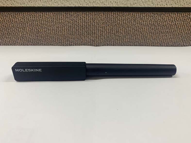
2AALG-NWP-F130
Aug 10, 2021Smart Pen
Equipment Class
DTS - Digital Transmission System2AALG-NWP-F80
Apr 04, 2021Neo Smartpen
Equipment Class
DTS - Digital Transmission System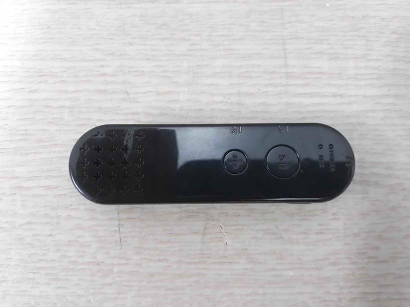
2AALG-NPR-R100
Apr 20, 2020NEO SMARTPEN
Equipment Class
DTS - Digital Transmission System