AAO210186314 Channel Family Radio Service
RadioShack Corporation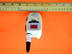
Click to zoom
Application Details
- Equipment Class
- FRF - Part 95 Family Radio Face Held Transmitter
- Date of Grant
- Apr 28, 2002
- Application Purpose
- Original Equipment
- Date of Application
- Mar 11, 2002
- Equipment Note
- 14 Channel Family Radio Service
- Frequency Range
- 462.56250000 - 467.71250000
- Company
- RadioShack Corporation
- Country
- United States
Documents & Files
Document Text
Text extracted from the exhibit documents filed with the FCC. Open a document above to read the original.
External Photos
Test SetupFCCID : AAO2101863 External Photo -front External Photo - rear
Internal Photos
Test SetupFCCID : AAO2101863 Internal Photo - 1 Internal Photo – 2 Test SetupFCCID : AAO2101863 Internal Photo – 3
Parts List/Tune Up Info
21_1863_Alignment_Procedure_A_0219Last Updated: 02-21-2002 Tandy Electronics ( China ) Limited Alignment Procedures Subject:FRS Cat. / Model No.:21-1863 RevisionA Total Page1 Designed ByBunny NG Approved By Standard Alignment Conditions Power Supply: 6 V DC Antenna Impedance: 50 ohm RF Signal Modulation:FM, 1 kHz sine wave with 1.5 kHz deviation Tuning Channel:Channel 4 (462.6375MHz) Audio Loading:32 ohm Audio Output Power:200 mW 1.TCXO Frequency Tuning The reference frequency 10.25MHz of the PLL is generated by the TCXO circuit (X801 and Q801). Since the TCXO frequency may be off tuned. We can measure output through TP7 by using spectrum analyzer to check the accuracy. 1.1 Tuning component: VC801 1.2 Equipment: Spectrum analyzer with high stability time base 1.3 Personnel : Skilful 1.4 Measure the 10.25MHz TCXO output signal to make sure it is accuracy: 1.4.1 Set channel 4 1.4.2 Press monitor key 1.4.3 Monitor the frequency of the TCXO output signal through the TP7 1.4.4 Tune the VC801 until the TCXO output carrier is at 10.25MHz ± 0.0005 MHz 2. VCO Tuning The tunable range of the VCO should be adjusted to make sure the control voltage of the VCO is enough margin for PLL locking 2.1 Tuning component: L201 2.2 Equipment: DVM for voltage measurement 2.3 Personnel : Skilful 2.4 Measure the control voltage of VCO to make sure there is enough margin for PLL margin: 2.4.1 Set to channel 1 2.4.2 Press Monitor key 2.4.3 Measure the voltage at TP3 and it should be higher than 0.4V 2.4.4 Set to channel 14 2.4.5 Press Monitor key 2.4.6 Measure the voltage at TP3 and it should be lower than 2.6V 3.Modulation Limit Tuning Set the transceiver to operate in Channel 4 and tune off the CTCSS tone, and connect the antenna output of the transceiver to the RF tester and monitor the modulation level. 21_1863_Alignment_Procedure_A_0219Last Updated: 02-21-2002 Input audio signal ( 1 kHz sine wave, 100 mV ) through the stereo jack to the transceiver. RF signal is transmitted. Adjust VR101 until the frequency deviation is around but less than 2 kHz 3.1 Tuning component : VR101 3.2 Equipment: Through stereo jack cable, connect the audio generator and transceiver together. Communication test set and modulation analsyer. 3.3 Personnel : Skilful 4.Squelch Tuning The squelch function of 21-1863 is realized by rectifying the demodulated noise signal. If the rectified noise level is higher than the threshold. A logic level will be generated to the MCU to determine the on and off of speaker. Hence by adjusting the level input to the rectifier, the squelch level can be controlled. 4.1 Tuning component: VR101 4.2 Equipment: Test jig with pin connected to speaker terminal Signal generator at –124dBm with 1KHz modulation source of 1.5KHz FM modulation 4.3 Personnel: Skiful 4.4 Testing procedure : 4.4.1 Input RF signal = 462.6375 MHz, frequency deviation = 1.5 kHz, modulating signal = 1 kHz. 4.4.2 Connect the transceiver to the RF generator and monitor the audio output from the speaker terminal. 4.4.3 Hold down MONITOR key and reduce the generator output power in ½ dB step until the SINAD meter shows 9-11 dB. 4.4.4 Rotate VR101 until the audio signal is JUST resumed from mute. 4.4.5 Reduce the RF generator output power until the audio signal is muted. Increase the output power in ½ dB step until the audio is just resumed. The SINAD meter should read 8-12 dB. 5.RF power Tuning In order to meet FCC requirement, the ERP output power should be tuned to 410mW. 5.1 Tuning component: R503 5.2 Equipment: Communication test set with RF power measurement option 5.3 Personnel: Skiful 5.4 Testing procedure: 5.4.1 Connect the DUT to the communication test set. 5.4.2 Set toe channel 4. 5.4.3 Press PTT key to activate the TX ON. 5.4.4 Set the R503 to lower or higher value to increase or decrease the RF power respectively.
Parts List/Tune Up Info
LvAssyPart NumberOperDescriptionQ'ty 711202180280A00AAMAIN PCB FR4 T1.6 4LAYERS1 711141089360A01AAAIR COIL ER0.4*1.65*4TN1 RefL 508 711141189100A01ABAIR COIL ER0.45*1.0*4T1 RefL 509 711141189130A01ACAIR COIL ER0.45*1.0*5TR4 RefL 001 L 002 L 006 L 201 711141189130A01ADAIR COIL ER0.45*1.0*5TR4 RefL 202 L 501 L 502 L 503 711142480080A01AEINDUCTOR BLM11B470SB1 RefL 507 711142581580A01AFINDUCTOR MGFI1608AR10K1 RefL 102 711142581590A01AGINDUCTOR MGCI1608H22NKT2 RefL 003 L 007 711142581610A01AHINDUCTOR MGCI1608H4N7DT1 RefL 505 711142581600A01AIINDUCTOR MGCI1608H33NKT1 RefL 005 711142581570A01AJCHIP INDUCTOR LQH43MN8R2K011 RefL 101 711154089120A01AKSMD TRIMMER TZC03P300A110T001 RefVC801 711177580090A01ALSEMI FIXED VR P0Z3AN-1-203N-T02 RefVR001 VR101 711187089650A01AMTACT SW RS-322R05B12 RefSW101 SW103 711CBNAK270JM02AACERAMIC CAPACI GRM39COG270J502 RefC 162 C 808 711CBNAK680JM02ABCERAMIC CAPACI GRM39COG680J501 RefC 132 711CBNAK681JM02ACCERAMIC CAPACI GRM39COG681J501 RefC 146 711CBNAK820JM02ADCERAMIC CAPACI GRM39COG820J502 RefC 148 C 015 711CBNAK100DM02AECERAMIC CAPACI GRM39COG100D504 RefC 008 C 211 C 512 C 811 711CBNAK101J*02AFCERAMIC CAPACI 1608 CH 50V 101J4 RefC 002 C 041 C 042 C 043 711CBNAK101J*02AGCERAMIC CAPACI 1608 CH 50V 101J2 RefC 205 C 516 711CBNAK110JM02AHCERAMIC CAPACI GRM39COG110J501 RefC 007 711CBNAK120JM02AICERAMIC CAPACI GRM39COG120J502 RefC 010 C 501 711CBNAK121JM02AJCERAMIC CAPACI GRM39COG121J502 RefC 804 C 155 711CBNAK150JM02AKCERAMIC CAPACI GRM39COG150J503 RefC 005 C 013 C 019 711CBNAK1R0CM03AACERAMIC CAPACI GRM39COG1R0C503 RefC 004 C 006 C 026 711CBNAK220JM03ABCERAMIC CAPACI GRM39COG220J502 RefC 509 C 809 711CBNAK221J*03ACCERAMIC CAPACI 1608 CH 50V 221J2 RefC 503 C 507 711CBNAK2R0CM03AECERAMIC CAPACI GRM39COG2R0C502 RefC 009 C 021 711CBNAK330JM03AFCERAMIC CAPACI 0603 330J501 RefC 029 711CBNAK3R0CM03AGCERAMIC CAPACI GRM39COG3R0C504 RefC 027 C 213 C 215 C 515 711CBNAK471JM03AHCERAMIC CAPACI GRM39COG471J505 RefC 031 C 040 C 102 C 104 C 711CBNAK4R0CM03AICERAMIC CAPACI GRM39COG4R0C502 RefC 028 C 048 711CBNAK560JM03AJCERAMIC CAPACI GRM39COG560J501 RefC 807 711CBNAK5R0CM03AKCERAMIC CAPACI GRM39COG5R0C502 RefC 016 C 207 711CBNAK6R0CM03ALCERAMIC CAPACI GRM39COG6R0C501 RefC 210 711CBNAK8R0DM04ABCERAMIC CAPACI GRM39COG8R0D503 RefC 003 C 204 C 505 711CBNAKR50CM04ACCERAMIC CAPACI GRM39COGR50C501 RefC 206 711CBNPK121JM04ADCERAMIC CAPACI 0603 UJ121J501 RefC 805 711CJNEK123KM04AICERAMIC CAPACI GRM39X7R123K503 RefC 306 C 313 C 318 711CJNEE224K*04AJCERAMIC CAPACI 0603X7R 224K103 RefC 311 C 327 C 131 711CJNEK223KM04AKCERAMIC CAPACI GRM39 X7R223K502 RefC 123 C 141 711CJNEK332KM04ALCERAMIC CAPACI GRM39 X7R332K502 RefC 150 C 321 711CJNEI683K*04AMCERAMIC CAP 0603 25V 683K1 RefC 304 711CJNEK272KM04ANCERAMIC CAPACI GRM39 X7R272K501 RefC 322 711CJNEK473KM05AACERAMIC CAPACI 0603 473K501 RefC 312 711CJNEK822KM05ABCERAMIC CAPACI GRM39 X7R822K501 RefC 320 711CJNEK222KM05ACCERAMIC CAPACI GRM39 X7R222K502 RefC 032 C 309 711CJNEE474K*05ADCERAMIC CAPACI 0603X7R474K101 RefC 201 711CJNEI333K*05AECERAMIC CAPACI 0603 25V 333K1 RefC 035 711CJNEK102K*05AFCERAMIC CAPACI 1608 B 50V 102K4 RefC 011 C 012 C 014 C 018 711CJNEK102K*05AGCERAMIC CAPACI 1608 B 50V 102K4 RefC 024 C 025 C 047 C 209 711CJNEK102K*05AHCERAMIC CAPACI 1608 B 50V 102K4 RefC 214 C 502 C 506 C 513 711CJNEK102K*05AICERAMIC CAPACI 1608 B 50V 102K2 RefC 517 C 518 711CJNEK102K*05AJCERAMIC CAPACI 1608 B 50V 102K3 RefC 119 C 121 C 159 711CJNEK103KM05AKCERAMIC CAPACI GRM39 X7R103K504 RefC 112 C 113 C 114 C 143 711CJNEK103KM05ALCERAMIC CAPACI GRM39 X7R103K504 RefC 171 C 172 C 316 C 319 711CJNEK103KM05AMCERAMIC CAPACI GRM39 X7R103K504 RefC 022 C 044 C 203 C 504 711CJNEK103KM05ANCERAMIC CAPACI GRM39 X7R103K502 RefC 153 C 120 711CJNAD225KM06AACERAMIC CAPACI GRM188R60J225KA01 RefC 202 711CJNPE105Z*06ABCERAMIC CAPACI 0603 10V 105Z4 RefC 033 C 034 C 111 C 154 711CJNPE105Z*06ACCERAMIC CAPACI 0603 10V 105Z4 RefC 157 C 129 C 151 C 164 711CJNPE105Z*06ADCERAMIC CAPACI 0603 10V 105Z4 RefC 301 C 302 C 303 C 310 711CJNPE105Z*06AECERAMIC CAPACI 0603 10V 105Z4 RefC 315 C 326 C 323 C 801 711CJNPG104ZM06AFCERAMIC CAPACI GRM39 Y5V104Z164 RefC 020 C 030 C 036 C 037 711CJNPG104ZM06AGCERAMIC CAPACI GRM39 Y5V104Z163 RefC 038 C 101 C 103 711CJNPG104ZM06AHCERAMIC CAPACI GRM39 Y5V104Z164 RefC 116 C 124 C 130 C 133 711CJNPG104ZM06AICERAMIC CAPACI GRM39 Y5V104Z163 RefC 135 C 136 C 802 711CJNPG104ZM06AJCERAMIC CAPACI GRM39 Y5V104Z164 RefC 156 C 160 C 314 C 324 711CJNEK153KM06AKCERAMIC CAPACI GRM39 X7R153K503 RefC 125 C 317 C 115 711RG0SN000J*07AAM-GLAZE RESIST RK 1/16C 000 o4 RefR 143 L 504 R 016 R 026 711RG0SN000J*07ABM-GLAZE RESIST RK 1/16C 000 o3 RefC 810 R 183 R 187 711RG0SN101J*07ACM-GLAZE RESIST RK1/16C 100 ohm4 RefR 013 R 030 R 033 R 211 711RG0SN101J*07ADM-GLAZE RESIST RK1/16C 100 ohm4 RefR 213 R 801 R 152 R 503 711RG0SN102J*07AEM-GLAZE RESIST RK1/16C 1 Kohm4 RefR 004 R 007 R 023 R 027 711RG0SN102J*07AFM-GLAZE RESIST RK1/16C 1 Kohm4 RefR 028 R 029 R 107 R 131 711RG0SN102J*07AGM-GLAZE RESIST RK1/16C 1 Kohm4 RefR 161 R 174 R 181 R 102 711RG0SN102J*07AHM-GLAZE RESIST RK1/16C 1 Kohm3 RefR 322 R 501 R 504 711RG0SN103J*07AIM-GLAZE RESIST RK1/16C 10 Kohm3 RefR 204 R 205 R 207 711RG0SN103J*07AJM-GLAZE RESIST RK1/16C 10 Kohm3 RefR 153 R 166 R 177 711RG0SN103J*07AKM-GLAZE RESIST RK1/16C 10 Kohm3 RefR 306 R 329 R 165 711RG0SN100J*07ALM-GLAZE RESIST RK 1/16C 10 o4 RefR 008 R 160 R 182 R 110 711RG0SN100J*07AMM-GLAZE RESIST RK 1/16C 10 o2 RefR 144 R 150 711RG0SN104J*08AAM-GLAZE RESIST RK1/16C 100 Kohm4 RefR 103 R 124 R 125 R 126 711RG0SN104J*08ABM-GLAZE RESIST RK1/16C 100 Kohm4 RefR 176 R 201 R 206 R 135 711RG0SN105J*08ACM-GLAZE RESIST RK1/16C 1 Mohm4 RefR 018 R 129 R 159 R 311 711RG0SN105J*08ADM-GLAZE RESIST RK1/16C 1 Mohm1 RefR 328 711RG0SN113J*08AEM-GLAZE RESIST RK 1/16C 11Ko1 RefR 315 711RG0SN153J*08AFM-GLAZE RESIST RK 1/16C 15Ko2 RefR 020 R 502 711RG0SN182J*08AGM-GLAZE RESIST RK1/16C 1R8 Kohm1 RefR 212 711RG0SN183J*08AHM-GLAZE RESIST RK1/16C 18 Kohm1 RefR 314 711RG0SN201J*08AIM-GLAZE RESI…
Text truncated - open the document above for the full version.
Test Report
Modulation Frequency Response 0.00 0.50 1.00 1.50 20070012001700220027003200370042004700 Modulation Frequency (Hz) Frequency Deviation (kHz) Modulation Frequency Response 0.00 0.50 1.00 1.50 2.00 20070012001700220027003200370042004700 Modulation Frequency (Hz) Modulation Index (%)
Test Report
Modulation Limiting Characteristic 0.00 0.50 1.00 1.50 2.00 475767778797107117127137 Modulation Input (dBSPL) Frequency Deviation (kHz) 500Hz 1000Hz 2500Hz 3125Hz
Test Report
• The test results rep orted in this rep ort shall refer only to the samp le actually tested and shall not refer or be deemed a refer to bulk from which such a samp le may be said to have been obtained. • This rep ort shall not be rep roduced excep t in full without p rior authorization from Intertek Testing Services Hong Kong Limit ed • For Terms And Conditions of the services, it can be p rovided up on request. Inte rte k Te sting Se rvice s Hong Kong Ltd. 2/F., Garment Centre, 576 Castle Peak Road, Kowloon, Hong Kong. Tel: (852) 2173 8888 Fax: (852) 2785 5487 RadioShack Corporation Application For Certification (FCC ID: AAO2101863) March 11, 2002 WO# 0200658 WL/Sandy March 11, 2002 INTERTEK TESTING SERVICES FCC ID: AAO2101863 i SUMMARY OF CONTENTS LIST OF EXHIBITS EXHIBIT 1 :General Description EXHIBIT 2 :System Test Configuration EXHIBIT 3 :RF Power Output EXHIBIT 4 :Modulation Characteristics EXHIBIT 5 :Occupied Bandwidth EXHIBIT 6 :Spurious Emission EXHIBIT 7 :Frequency Stability EXHIBIT 8 :Technical Specifications EXHIBIT 9 :Product Labelling EXHIBIT 10 :Photographs EXHIBIT 11: Instruction Manual EXHIBIT 12: Tune Up Procedure EXHIBIT 13: Part List INTERTEK TESTING SERVICES FCC ID: AAO2101863 ii MEASUREMENT/TECHNICAL REPORT Application: RadioShack Corporation Trade Name/Model No : RadioShack 21-1863 Date: March 11, 2002 This report concerns (check one:)Original Grant X Class II Change Equipment Type: Family Radio Service, FRS Deferred grant requested per 47 CFR 0.457(d)(1)(ii)? Yes No X If yes, defer until: date Company Name agrees to notify the Commission by: date of the intended date of announcement of the product so that the grant can be issued on that date. Report prepared by:Wilson Loke Intertek Testing Services 2/F., Garment Centre, 576 Castle Peak Road, Kowloon, Hong Kong. Phone: 852-2173-8575 Fax:852-2745-8306 INTERTEK TESTING SERVICES FCC ID: AAO2101863 iii Table of Contents 1.0 General Description .......................................................................................................... 2 1.1 Product Description ...................................................................................................... 2 1.2 Related Submittal(s) Grants .......................................................................................... 3 1.3 Test Methodology ......................................................................................................... 3 1.4 Test Facility................................................................................................................... 3 2.0 System Test Configuration ................................................................................................ 5 2.1 Justification ...................................................................................................................5 2.2 EUT Exercising Software .............................................................................................. 6 2.3 Special Accessories ....................................................................................................... 6 2.4 Measurement Uncertainty ............................................................................................. 6 2.5 Equipment Modification ................................................................................................ 6 3.0 RF Output Power (Section 95.639(d)) ............................................................................. 8 4.0 Modulation Characteristics (Section 95.637(a)) ........................................................... 12 4.1 Modulation Frequiency Response ............................................................................... 13 4.2 Modulation Limiting Characteristic............................................................................. 15 4.3 Audio Low Pass Filter Response................................................................................. 17 5.0 Occupied Bandwidth (Section 95.633(c)) ..................................................................... 19 6.0 Spurious Emission (Section 95.635(b)) .......................................................................... 21 6.1 Field Strength of Spurious Radiation .......................................................................... 22 7.0 Frequency Stability (Section 95.627) ............................................................................. 28 7.1 Frequency Tolerance ................................................................................................... 29 7.2 Temperature Extreme Condition ................................................................................. 31 7.3 Voltage Extreme Condition ......................................................................................... 34 8.0 Technical Specifications .................................................................................................. 37 9.0 Product Labelling ............................................................................................................ 41 10.0 Equipment Photographs ............................................................................................... 44 11.0 Instruction Mannal ........................................................................................................ 46 12.0 Tune Up Procedure ....................................................................................................... 48 13.0 Part List .......................................................................................................................... 50 INTERTEK TESTING SERVICES FCC ID: AAO2101863 iv List of attached file Exhibit typeFile DescriptionFilename Operation DescriptionTechnical Descriptiondescri.pdf Test ReportBandwidth Plotbw.pdf Test ReportModulation Frequency Responsemfr.pdf Test ReportModulation Limit Characteristicmlc.pdf Test ReportSpurious Emissionspurious.pdf Block DiagramBlock Diagramblock.pdf SchematicsCircuit Diagramcircuit.pdf ID Label/LocationLabel …
Text truncated - open the document above for the full version.
Test Setup Photos
Test SetupFCCID : AAO2101863 Radiated -front Radiated - rear
Contact Information
Applicant
Elizabeth Granados(Regulatory Affairs Manager)
Technical Contact
Intertek Testing Services Hong Kong Ltd.Wilson Loke
[email protected](852) 21738575
2/F., Garment Centre, · Kowloon · Hong Kong
Non-Technical Contact
Intertek Testing Services Hong Kong Ltd.Wilson Loke
[email protected](852) 21738575
Test Firm
Intertek Testing Services Hong KongBilly Chow
Technical Specifications
| # | Rule Parts | Frequency Range | Power Output | Emission | Tolerance |
|---|---|---|---|---|---|
| 1 | 95B | 462.5625 MHz - 467.7125 MHz | 410.00 mW | 9K60F3E | 2.5000000000 ppm |
Other Applications from RadioShack Corporation
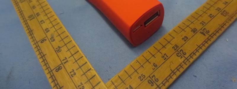
AAO2302500
Feb 10, 2015Bluetooth Power Bank
Equipment Class
DXX - Part 15 Low Power Communication Device Transmitter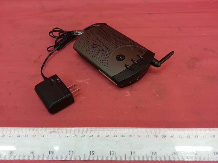
AAO4300124C
May 02, 2013900MHz Wireless Intercom
Equipment Class
DXT - Part 15 Low Power Transceiver, Rx Verified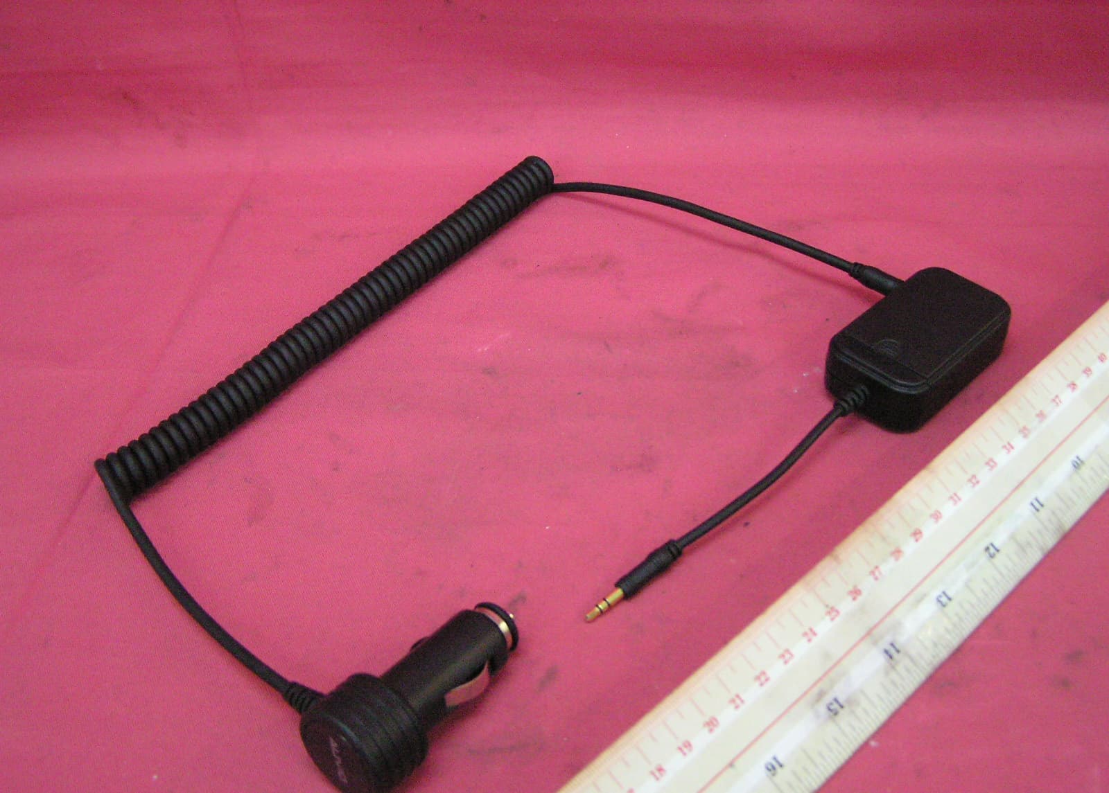
AAO1200876
Nov 30, 2011Universal FM Transmitter
Equipment Class
DXX - Part 15 Low Power Communication Device Transmitter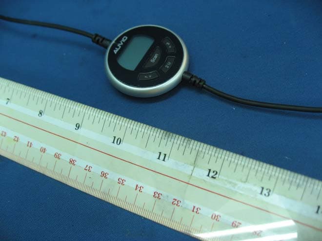
AAO1200962
Aug 02, 2011Universal FM Transmitter
Equipment Class
DXX - Part 15 Low Power Communication Device Transmitter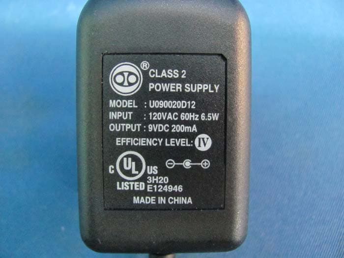
AAO1500044T
Apr 02, 20112.4GHz Digital Wireless Rear Speaker Kit - Transmitter
Equipment Class
DSS - Part 15 Spread Spectrum Transmitter