AAO210186414 Channel Family Radio Service
RadioShack Corporation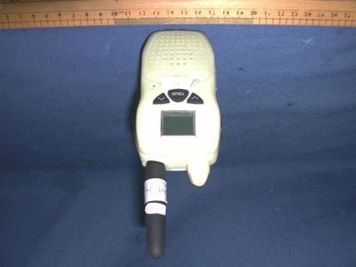
Click to zoom
Application Details
- Equipment Class
- FRF - Part 95 Family Radio Face Held Transmitter
- Date of Grant
- Apr 28, 2002
- Application Purpose
- Original Equipment
- Date of Application
- Mar 11, 2002
- Equipment Note
- 14 Channel Family Radio Service
- Frequency Range
- 462.56250000 - 467.71250000
- Company
- RadioShack Corporation
- Country
- United States
Documents & Files
Document Text
Text extracted from the exhibit documents filed with the FCC. Open a document above to read the original.
Users Manual
1 21-1864 14 Channel Personal FRS 2-Way Radio with 38 Quiet Code, Vibrate, Splash Proof and VOX Family Radio Service (FRS) is a license-free, two-way, short-range voice radio service that lets families and groups keep in touch with each other on specific reserved channels. Your RadioShack 14 Channel Personal FRS 2-Way Radio is a lightweight, palm-sized radio you can use to talk with another person who has a FRS radio set to the same frequency as your radio. Your radio has auto-squelch, so you will not hear anything on a channel unless someone is transmitting nearby on the same channel. You can use MON (monitor) key to temporarily turn off auto-squelch to hear weaker, distant transmissions. You can connect an optional speaker/microphone and earphone to the radio (neither supplied, available at your local RadioShack store). Your radio’s display has a backlight that turns on for about 10 seconds when you press any key except PTT. Your radio’s other features include: 14 Channels – provide clear communications for up to two miles. Channel Scan – use to find other FRS users. 38 Quiet Code – eliminates interference from other radios that are not tuned to the same channel and quiet code as your radio. Courtesy Tone – at the end of conversation, it generates for end of message acknowledgement. Key Beep – short beep generation for key pressed acknowledgement (except PTT and MON). Lock – locks ^/SCAN, v/CALL and QUIET/MENU. Vibration Alert – vibrates for 2 seconds when receiving signal if the radio is idle for more than 30 seconds. Splash Proof (JIS level 4) – provide excellent waterproof and capability. Voice Operated Transmission (VOX) – enables standalone usage and works with handsfree accessory. INSTALLING BATTERIES Your radio requires four AAA alkaline or rechargeable nickel-cadmium (Ni-Cd) / nickel-metal hydride (Ni-MH) batteries (not supplied) for power. For the best performance and longest life, we recommend RadioShack batteries. Cautions: 0 Use only fresh batteries of the required size and recommended type. 0 Do not mix old and new batteries, different types of batteries (alkaline or rechargeable), or rechargeable batteries of different capacities. 1. Rotate VOL/OFF counterclockwise until it clicks to turn off the radio. 2. Pull down the latch on the battery compartment cover, then remove the cover. 2 3. Slide CHARGE ON/OFF inside the battery compartment to OFF (for alkaline batteries) or ON (for Ni-Cd or Ni-MH rechargeable batteries). Warning: Never install non-rechargeable batteries when CHARGE ON/OFF is set to ON. Non-rechargeable batteries can get hot or explode if you try to recharge them. 4. Install four AAA batteries according to the polarity symbols (+ and -) marked inside. 5. Replace the cover and push the latch up until it clicks, then rotate VOL/OFF clockwise until it clicks to turn on the radio. The battery icon’s segments ( ) display to show how much power remain. When the last segment flashes, replace alkaline batteries or recharge Ni-Cd or Ni-MH batteries. Warning: Dispose of old batteries promptly and properly. Do not burn or bury them. Caution: If you do not plan to use the radio for a month or longer, remove the batteries. Batteries can leak chemicals that can destroy electronic parts. Recharging Ni-Cd or Ni-MH Batteries Warning: Do not attempt to charge alkaline batteries. Non-rechargeable batteries can get hot or explode if you try to recharge them. The radio’s DC 6V jack is for charging Ni-Cd or Ni-MH batteries and powering the radio. You can recharge Ni-Cd or Ni-MH batteries inside the radio at home or vehicle, using a 6V, 600mA AC or DC adapter and a size F Adaptaplug TM connector (neither supplied, both available at your local RadioShack store). Cautions: 0 You must use a Class 2 power source that supplies regulated 6V DC (Not more than 6V) and delivers at least 600mA. Its center tip must be set to positive and its plug must fit the radio’s DC 6V jack. Using an adapter that does not meet these specifications could damage the radio or the adapter. 0 Always connect the adapter to the radio before you connect it to an external power source (such as an AC outlet or a vehicle cigarette-lighter socket). When you finish, disconnect the adapter from the power source before you disconnect it from the radio. 1. Rotate VOL/OFF fully counterclockwise to turn off the radio. 2. Pull down the latch on the battery compartment cover and remove the cover. 3. Set CHARGE ON/OFF to ON. 4. Place four Ni-Cd or Ni-MH batteries in the compartment according to the polarity symbols (+ and -) marked inside. Then replace the cover and push the latch up until it clicks. 5. Attach the Adaptaplug to the adapter so TIP reads positive (+). 6. Connect the Adaptaplug’s other end to the radio’s DC 6V jack and plug the adapter into a standard AC outlet or vehicle’s power source. Complete charging takes about 10 hours. When charging is complete, unplug the AC or DC adapter from the power source, then disconnect it from the radio’s DC 6V jack. 3 Note: Ni-MH batteries take longer to charge than Ni-Cd batteries. Important: The EPA certified RBRC® Battery Recycling Seal on the nickel-cadmium (Ni-Cd) battery indicates RadioShack is voluntarily participating in an industry program to collect and recycle these batteries at the end of their useful life, when taken out of service in the United States or Canada. The RBRC program provides a convenient alternative to placing used Ni0Cd batteries into the trash or the municipal waste stream, which may be illegal in your area. Please call 1-800-THE-SHACK (1-800-843-7422) for information on Ni-Cd battery recycling and disposal bans/restrictions in your area. RadioShack’s involvement in this program is part of the company’s commitment to preserving our environment and conserving our natural resources. OPERATION A QUICK LOOK AT YOUR RADIO (21-1864_FrontView.eps & 21-1864_SideView.eps) Callouts: PTT – Hold down and speak into the microphone to transmit. TX appears. Releas…
Text truncated - open the document above for the full version.
Block Diagram
TMP47C222 /422 VOXSCANVIBRATOR BackLight Power Control Unit Resistor Combiner I/O /BACK_LIGHT /TX_ON /VCO_CTFIL_ON PLL_DATA/EE_DATA /MIC_ON LCD Common Drive LCD Segment Drive I/O CTCSS_TONE3CTCSS_TONE2 CTCSS_TONE LPF AUDIO_IN TONE_IN 3V5 HPF /RX_ON AUDIO_IN /TX_ON /RX_ON /TX_ON FILITERED_MIC_INFILTERED_AUDIO_IN Counter 1Counter 2 /PULSE CALL_TONE/ KEY_TONE AMP AUDIO_ON FILTERED_AUDIO_IN PA BAT_6V VCO PLL S1T8825 TX_MOD PLL_STB EEPROM 24C02 IF DEMOD DBL 5018 AUDIO_IN MUTE /RX_ON Vibr ator VOX Detector KEY SWITCH MODE UP/SCAN DOWN/CALL PTT I/O A/D BATTERY_DET XOUT XIN 4MHz RESONATOR MIC_IN VOLUME CONTROL 21-1864 14 Channel MID Range FRS with CTCSS and VOX High Pass Filter Low Pass Filter SPEAKER MIC MIC_IN RF Front End CTCSS_TONE1 TONE_IN PLL_DATA/EE_DATA/MIC_ON PLL_CLK/EE_CLK VIBRATOR/MODE PLL_DATA/EE_DATA/MIC_ON PLL_CLK/EE_CLK PA DRVIER LPF TX_LO 3V5 10.25MHz TCXO TX_3V5 LNA 464MHz SAW FILTER PLL_CTFIL_3V5 10.25MHz 10.7MHz CRYSTAL FILTER RX LO LPF 3V5 LPF CALL_TONE/ kEY_TONE PRE- EMPHASIS & AMP FILTERED_MIC_IN VOX Hi/Lo SELECTION CHARGING CIRCUIT CLA 6V DC INPUT BAT CALL_TONE/ KEY_TONE I/O VT RX_3V5 RX_3V5 450KHz FIL RX_3V5 450KHz Discriminator CALL_TONE/KEY_TONE
External Photos
Test SetupFCCID : AAO2101864 External Photo -front External Photo - rear
Internal Photos
Test SetupFCCID : AAO2101864 Internal Photo - 1 Internal Photo - 2 Test SetupFCCID : AAO2101864 Internal Photo - 3
Operational Description
1 of 3 TRANSCEIVER CIRCUIT DESCRIPTION 21-1864 is a single board design which consists both RF and Baseband part. RF PART The RF part contains all necessary RF circuit. It converts the RF signal picked up by the antenna to demodulated analogue signal for further processing. Besides, the base band analogue signal, including voice and CTCSS tone, will use to FM-modulate the RF carrier during transmission. The main building blocks of the RF part includes a LNA, a SAW filter, a Mixer, a VCO, a Ceramic filter, FM-IF detector circuit and power amplifier for transmission. Among those building blocks, the RF circuit can be divided into two sections. A: RX section This product employs traditional double conversion superheterodyne architecture with the following functional blocks: 1.The LNA with cascade configuration is composed by transistor Q1 and Q2. It has the merits of low noise figure and high insertion gain. 2.The LO signal is generated by VCO which is phase locked with the reference TCXO circuit (X801) at the 10.25MHz. The TCXO can stabilize the frequency of the oscillator within 2.5ppm from –20 to +50 degree C. The LO signal is amplified by transistor Q4 and coupled to the mixer (Q3) for RF to IF conversion. The LO frequency is controlled by the PLL (U2) after received command from MCU (U101). 3.The first image rejection filter, F1, is a SAW (surface acoustic wave) device, with the merits of having low insertion loss and high stop band attenuation. 4.The mixer is a common emitter configured transistor Q3. It converts RF signal to an IF of 10.7MHz. This IF will further be filtered by the crystal filter F2. 5.Inside the FM-IF chip, the IF signal is further down converted to 450KHz second IF demodulation. The second LO signal is generated by the reference oscillator of the PLL chip. The second IF signal is also further filtered by the ceramic filter for better adjacent channel rejection response. The second IF signal is then demodulated by the resonator X1. The demodulated audio signal will be transferred to the main board for further processing. 6.By trimming the VR1, the audio noise signal level to the internal comparator of the FM IF chip 3361 can be varied. Since the comparator output was used to determine the status of received signal quality, and hence the squelch level can be adjusted. B: TX section 1.The TX carrier is also generated by the VCO with the control from PLL chip. The VCO signal is coupled to amplifier Q501 and Q502. The output signal will be boosted up by the Class-B power amplifier Q503, Q504 and Q505. 2 of 3 BASE BAND PART The digital part controlled all the base band signal including voltage regulation, battery charging, keyboard input, call tone generator, CTCSS encode/decode, VOX, motor circuit and display. 1.Voltage regulation: The operating voltage of the circuit is stabilized by the 3.5V voltage regulator U103. 2.Power management: In order to extend the battery life of the unit, unnecessary circuit during different operation modes will be shut down for power saving. The on and off mechanism is controlled by the MCU with the help of some analogue switches which are realized by transistors: They can be classified as : a.Q101VCO circuit b.Q102RX RF circuit c.Q103TX RF circuit d.Q112MIC circuit 3.Display: The channel number, Quiet code, C-Tone icon, TX icon, Lock icon, battery icon will be prompted to the users by LCD. There is also a backlite LED for better visual effect under dim environment. 4.Keyboard input: The transceiver had several function keys such as MENU(QUIET), UP(SCAN), DOWN(CALL), PTT and Monitor switch. During the operation, all these function key input will be handled by the MCU. 5.Memory: The memory or setting of the transceiver is stored in the EEPROM U102. 6.Low battery dectection: It is realized by the internal A/D of the MCU during power saving mode. 7.High pass filter, Pre-emphasis, Limiter and Low pass filter: The acoustic input transducer by the microphone will go through a 300Hz high pass filter first. This HPF is used to reduced the interference between the user voice and CTCSS tone. This HPF is realized by U302. The pre-emphasis is realized by capacitor C141. The pre-emphasis responses follow the recommendation of EIA standard. After the pre-emphasis stage, limiter and low pass filter are inevitable which are realized by U106. 8.De-emphasis, High pass filter and volume control: The demodulated base band signal from RX section needs to be de-emphasised first. Then the signal will pass through the High pass filter for clear audio signal recovery. This section is realized by U302. This signal will feed to the audio amplifier U104 for power boosting. The volume level is control by the rotary resistor VR106. 9.CTCSS tone generator: Three different signals from MCU were connected to the external resistor network to generate the CTCSS tone. This pure CTCSS tone will add to the VCO for FM modulation. 10.CTCSS tone decode: The demodulated base band signal from RX section will pass through the low pass filter U301. The CTCSS tone received will be transformed to square wave by this filter. This signal will be used for decoding. The MCU will decode this signal by checking its frequency and duty cycle. 3 of 3 11.MCU internal clock and reset: The reset is realized by D104. Since the CTCSS tone is reference with the internal clock of the MCU, 4 MHz ceramic resonator is used as the main resonating element in order to have a better accuracy. 12.Battery charging: This transceiver can use with 6V DC regulated external CLA adaptor. The transceiver can function normally during charging the rechargeable battery in the compartment. 13.Automatic Squelch: The squelch detection signal from RX section will alert the MCU to mute the speaker. The squelch level is controlled by VR1 on the RF part. 14.VOX circuit: The MIC signal is amplified and rectified by amplifier Q107 and coupled to MCU for level detection. 15.Motor circuit: The motor is controlled by the switching …
Text truncated - open the document above for the full version.
Parts List/Tune Up Info
21_1864_Alignment_Procedure_A_0226Last Updated: 02-26-2002 Tandy Electronics ( China ) Limited Alignment Procedures Subject:FRS Cat. / Model No.:21-1864 RevisionA Total Page1 Designed ByBunny NG Approved By Standard Alignment Conditions Power Supply: 6 V DC Antenna Impedance: 50 ohm RF Signal Modulation:FM, 1 kHz sine wave with 1.5 kHz deviation Tuning Channel:Channel 4 (462.6375MHz) Audio Loading:32 ohm Audio Output Power:200 mW 1.TCXO Frequency Tuning The reference frequency 10.25MHz of the PLL is generated by the TCXO circuit (X801 and Q801). Since the TCXO frequency may be off tuned. We can measure output through TP7 by using spectrum analyzer to check the accuracy. 1.1 Tuning component: VC801 1.2 Equipment: Spectrum analyzer with high stability time base 1.3 Personnel : Skilful 1.4 Measure the 10.25MHz TCXO output signal to make sure it is accuracy: 1.4.1 Set channel 4 1.4.2 Press monitor key 1.4.3 Monitor the frequency of the TCXO output signal through the TP7 1.4.4 Tune the VC801 until the TCXO output carrier is at 10.25MHz ± 0.0005 MHz 2. VCO Tuning The tunable range of the VCO should be adjusted to make sure the control voltage of the VCO is enough margin for PLL locking 2.1 Tuning component: L201 2.2 Equipment: DVM for voltage measurement 2.3 Personnel : Skilful 2.4 Measure the control voltage of VCO to make sure there is enough margin for PLL margin: 2.4.1 Set to channel 1 2.4.2 Press Monitor key 2.4.3 Measure the voltage at TP3 and it should be higher than 0.4V 2.4.4 Set to channel 14 2.4.5 Press Monitor key 2.4.6 Measure the voltage at TP3 and it should be lower than 2.6V 3.Modulation Limit Tuning Set the transceiver to operate in Channel 4 and tune off the CTCSS tone, and connect the antenna output of the transceiver to the RF tester and monitor the modulation level. 21_1864_Alignment_Procedure_A_0226Last Updated: 02-26-2002 Input audio signal ( 1 kHz sine wave, 100 mV ) through the stereo jack to the transceiver. RF signal is transmitted. Adjust VR101 until the frequency deviation is around but less than 2 kHz 3.1 Tuning component : VR101 3.2 Equipment: Through stereo jack cable, connect the audio generator and transceiver together. Communication test set and modulation analsyer. 3.3 Personnel : Skilful 4.Squelch Tuning The squelch function of 21-1863 is realized by rectifying the demodulated noise signal. If the rectified noise level is higher than the threshold. A logic level will be generated to the MCU to determine the on and off of speaker. Hence by adjusting the level input to the rectifier, the squelch level can be controlled. 4.1 Tuning component: VR101 4.2 Equipment: Test jig with pin connected to speaker terminal Signal generator at –124dBm with 1KHz modulation source of 1.5KHz FM modulation 4.3 Personnel: Skiful 4.4 Testing procedure : 4.4.1 Input RF signal = 462.6375 MHz, frequency deviation = 1.5 kHz, modulating signal = 1 kHz. 4.4.2 Connect the transceiver to the RF generator and monitor the audio output from the speaker terminal. 4.4.3 Hold down MONITOR key and reduce the generator output power in ½ dB step until the SINAD meter shows 9-11 dB. 4.4.4 Rotate VR101 until the audio signal is JUST resumed from mute. 4.4.5 Reduce the RF generator output power until the audio signal is muted. Increase the output power in ½ dB step until the audio is just resumed. The SINAD meter should read 8-12 dB. 5.RF power Tuning In order to meet FCC requirement, the ERP power should be tuned to 420mW. 5.1 Tuning component: R503 5.2 Equipment: Communication test set with RF power measurement option 5.3 Personnel: Skiful 5.4 Testing procedure: 5.4.1 Connect the DUT to the communication test set. 5.4.2 Set toe channel 4. 5.4.3 Press PTT key to activate the TX ON. 5.4.4 Set the R503 to lower or higher value to increase or decrease the RF power respectively.
Schematics
T497_WS_0226.sch-1 - Tue Feb 26 15:22:08 2002 T497_WS_0226.sch-2 - Tue Feb 26 15:27:14 2002 T497_WS_0226.sch-3 - Tue Feb 26 15:27:53 2002
Test Report
Modulation Frequency Response 0.00 0.50 1.00 1.50 20070012001700220027003200370042004700 Modulation Frequency (Hz) Frequency Deviation (kHz) Modulation Frequency Response 0.00 0.50 1.00 1.50 2.00 20070012001700220027003200370042004700 Modulation Frequency (Hz) Modulation Index (%)
Test Report
Modulation Limiting Characteristic 0.00 0.50 1.00 1.50 2.00 475767778797107117127137 Modulation Input (dBSPL) Frequency Deviation (kHz) 500Hz 1000Hz 2500Hz 3125Hz
Test Report
• The test results rep orted in this rep ort shall refer only to the samp le actually tested and shall not refer or be deemed a refer to bulk from which such a samp le may be said to have been obtained. • This rep ort shall not be rep roduced excep t in full without p rior authorization from Intertek Testing Services Hong Kong Limit ed • For Terms And Conditions of the services, it can be p rovided up on request. Inte rte k Te sting Se rvice s Hong Kong Ltd. 2/F., Garment Centre, 576 Castle Peak Road, Kowloon, Hong Kong. Tel: (852) 2173 8888 Fax: (852) 2785 5487 RadioShack Corporation Application For Certification (FCC ID: AAO2101864) March 11, 2002 WO# 0200662 WL/Sandy March 11, 2002 INTERTEK TESTING SERVICES FCC ID: AAO2101864 i SUMMARY OF CONTENTS LIST OF EXHIBITS EXHIBIT 1 :General Description EXHIBIT 2 :System Test Configuration EXHIBIT 3 :RF Power Output EXHIBIT 4 :Modulation Characteristics EXHIBIT 5 :Occupied Bandwidth EXHIBIT 6 :Spurious Emission EXHIBIT 7 :Frequency Stability EXHIBIT 8 :Technical Specifications EXHIBIT 9 :Product Labelling EXHIBIT 10 :Photographs EXHIBIT 11: Instruction Manual EXHIBIT 12: Tune Up Procedure EXHIBIT 13: Part List INTERTEK TESTING SERVICES FCC ID: AAO2101864 ii MEASUREMENT/TECHNICAL REPORT Application: RadioShack Corporation Trade Name/Model No :RadioShack 21-1864 Date: March 11, 2002 This report concerns (check one:)Original Grant X Class II Change Equipment Type: Family Radio Service, FRS Deferred grant requested per 47 CFR 0.457(d)(1)(ii)? Yes No X If yes, defer until: date Company Name agrees to notify the Commission by: date of the intended date of announcement of the product so that the grant can be issued on that date. Report prepared by:Wilson Loke Intertek Testing Services 2/F., Garment Centre, 576 Castle Peak Road, Kowloon, Hong Kong. Phone: 852-2173-8575 Fax:852-2745-8306 INTERTEK TESTING SERVICES FCC ID: AAO2101864 iii Table of Contents 1.0 General Description .......................................................................................................... 2 1.1 Product Description ...................................................................................................... 2 1.2 Related Submittal(s) Grants .......................................................................................... 3 1.3 Test Methodology ......................................................................................................... 3 1.4 Test Facility................................................................................................................... 3 2.0 System Test Configuration ................................................................................................ 5 2.1 Justification ...................................................................................................................5 2.2 EUT Exercising Software .............................................................................................. 6 2.3 Special Accessories ....................................................................................................... 6 2.4 Measurement Uncertainty ............................................................................................. 6 2.5 Equipment Modification ................................................................................................ 6 3.0 RF Output Power (Section 95.639(d)) ............................................................................. 8 4.0 Modulation Characteristics (Section 95.637(a)) ........................................................... 12 4.1 Modulation Frequiency Response ............................................................................... 13 4.2 Modulation Limiting Characteristic............................................................................. 15 4.3 Audio Low Pass Filter Response................................................................................. 17 5.0 Occupied Bandwidth (Section 95.633(c)) ..................................................................... 19 6.0 Spurious Emission (Section 95.635(b)) .......................................................................... 21 6.1 Field Strength of Spurious Radiation .......................................................................... 22 7.0 Frequency Stability (Section 95.627) ............................................................................. 28 7.1 Frequency Tolerance ................................................................................................... 29 7.2 Temperature Extreme Condition ................................................................................. 31 7.3 Voltage Extreme Condition ......................................................................................... 34 8.0 Technical Specifications .................................................................................................. 37 9.0 Product Labelling ............................................................................................................ 41 10.0 Equipment Photographs ............................................................................................... 44 11.0 Instruction Mannal ........................................................................................................ 46 12.0 Tune Up Procedure ....................................................................................................... 48 13.0 Part List .......................................................................................................................... 50 INTERTEK TESTING SERVICES FCC ID: AAO2101864 iv List of attached file Exhibit typeFile DescriptionFilename Operation DescriptionTechnical Descriptiondescri.pdf Test ReportBandwidth Plotbw.pdf Test ReportModulation Frequency Responsemfr.pdf Test ReportModulation Limit Characteristicmlc.pdf Test ReportSpurious Emissionspurious.pdf Block DiagramBlock Diagramblock.pdf SchematicsCircuit Diagramcircuit.pdf ID Label/LocationLabel A…
Text truncated - open the document above for the full version.
Test Report
Audio Low Pass Filter Response (Model: 21-1864) -60.0 -50.0 -40.0 -30.0 -20.0 -10.0 0.0 10.0 110100 Frequency (kHz) dB relative to 1 kHz LPF Response TIA/EIA-603
Test Setup Photos
Test SetupFCCID : LBBFS2000AT Radiated -front Radiated - rear
Contact Information
Applicant
Elizabeth Granados(Regulatory Affairs Manager)
Technical Contact
Intertek Testing Services Hong Kong Ltd.Wilson Loke
[email protected](852) 21738575
2/F., Garment Centre, · Kowloon · Hong Kong
Non-Technical Contact
Intertek Testing Services Hong Kong Ltd.Wilson Loke
[email protected](852) 21738575
Test Firm
Intertek Testing Services Hong KongBilly Chow
Technical Specifications
| # | Rule Parts | Frequency Range | Power Output | Emission | Tolerance |
|---|---|---|---|---|---|
| 1 | 95B | 462.5625 MHz - 467.7125 MHz | 420.00 mW | 9K00F3E | 2.5000000000 ppm |
Other Applications from RadioShack Corporation
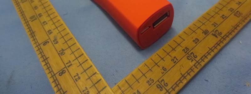
AAO2302500
Feb 10, 2015Bluetooth Power Bank
Equipment Class
DXX - Part 15 Low Power Communication Device Transmitter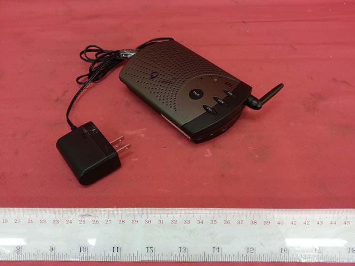
AAO4300124C
May 02, 2013900MHz Wireless Intercom
Equipment Class
DXT - Part 15 Low Power Transceiver, Rx Verified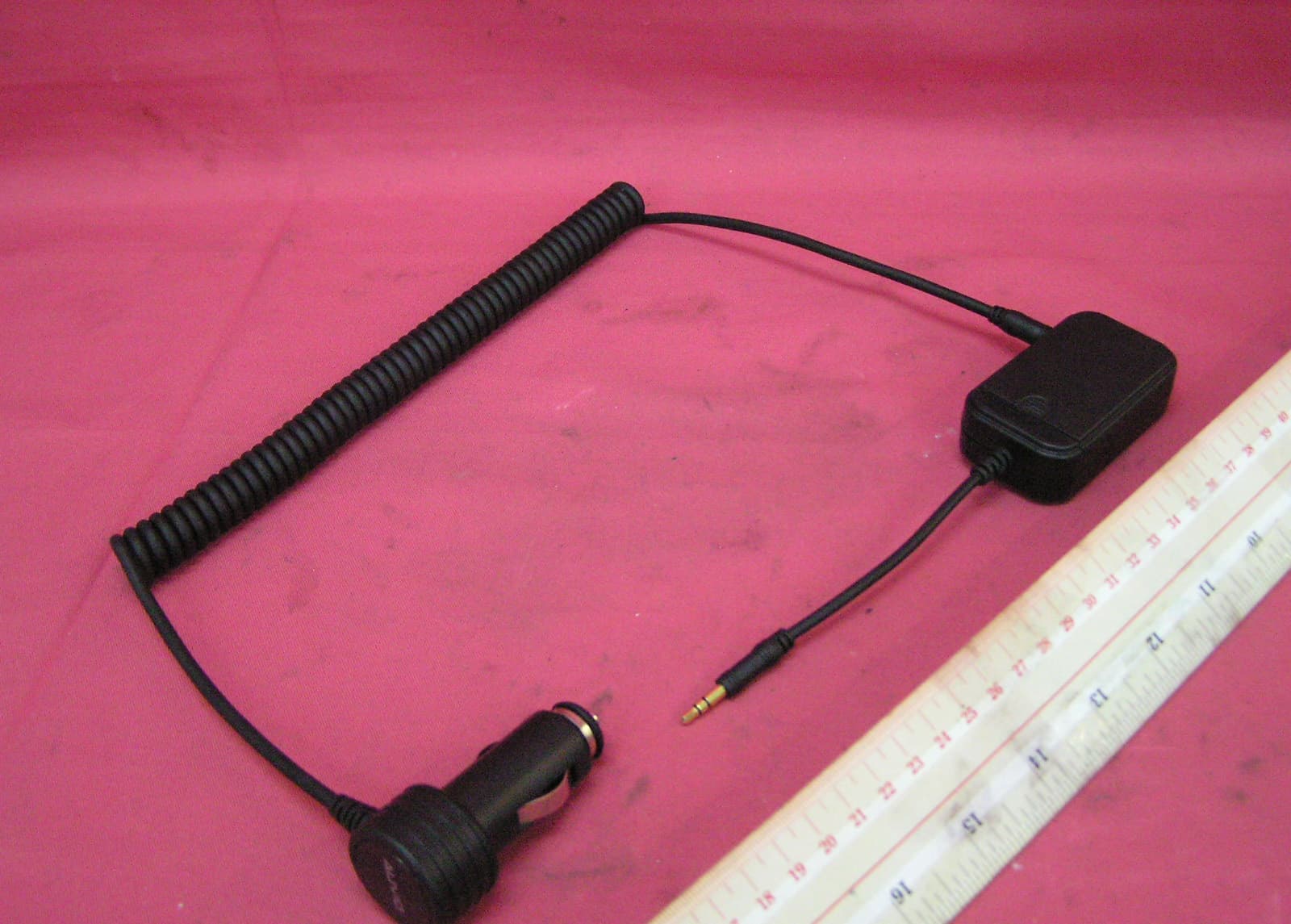
AAO1200876
Nov 30, 2011Universal FM Transmitter
Equipment Class
DXX - Part 15 Low Power Communication Device Transmitter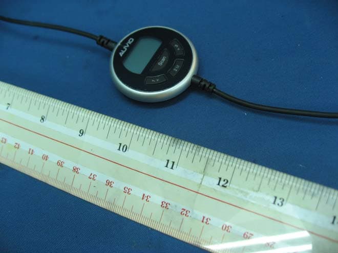
AAO1200962
Aug 02, 2011Universal FM Transmitter
Equipment Class
DXX - Part 15 Low Power Communication Device Transmitter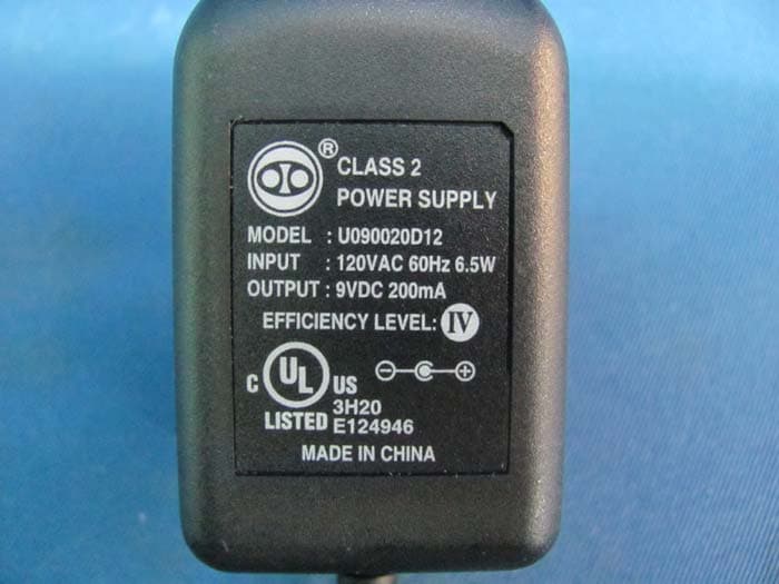
AAO1500044T
Apr 02, 20112.4GHz Digital Wireless Rear Speaker Kit - Transmitter
Equipment Class
DSS - Part 15 Spread Spectrum Transmitter