AAO210190522 Channel GMRS/FRS 2-Way Radio
RadioShack Corporation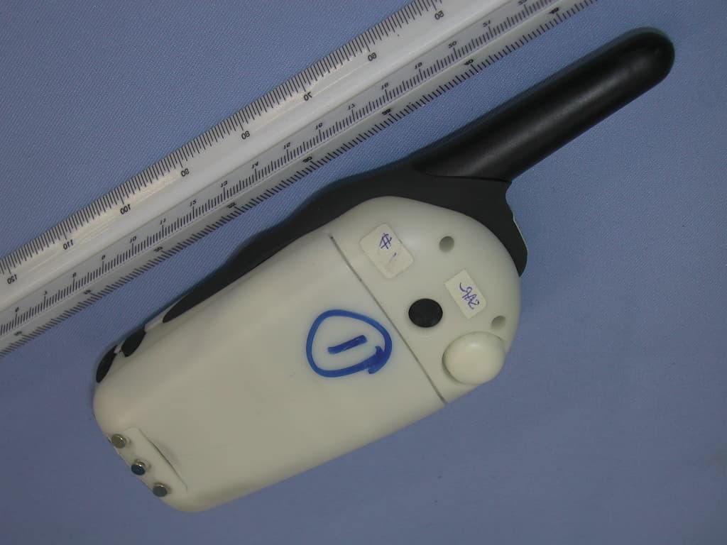
Click to zoom
Application Details
- Equipment Class
- FRF - Part 95 Family Radio Face Held Transmitter
- Date of Grant
- May 27, 2003
- Application Purpose
- Original Equipment
- Date of Application
- May 27, 2003
- Equipment Note
- 22 Channel GMRS/FRS 2-Way Radio
- Frequency Range
- 467.56250000 - 467.71250000
- Company
- RadioShack Corporation
- Country
- United States
Documents & Files
Document Text
Text extracted from the exhibit documents filed with the FCC. Open a document above to read the original.
Block Diagram
S3F8235 VOX MISS ID VIBRATOR BackLight Power Control Unit Resistor Combiner I/O /BACK_LIGHT /TX_ON /VCO_ON LCD Common Drive LCD Segment Drive 4 common 8 segments I/O CTCSS_TONE3CTCSS_TONE2 CTCSS_TONE Counter 1Counter 2 /PULSE CALL /KEY_TONE AMP AUDIO_ON FILTERED_AUDIO_IN PA BAT_6V VCO PLL TA31202 TX_MOD PLL_STB EEPROM 24C02 IF DEMOD DBL 5019 AUDIO_IN MUTE /RX_ON Vibrator VOX Detector KEY SWITCH MENU UP DOWN PTT I/O A/D BATT ERY_DET XOUT XIN 4MHz RESONATOR VOLUME CONTROL 21-1905 22 Channel, 0.5W/2W, CTCSS and VOX 32 ohm SPEAKER MIC MIC_IN RF Front End CTCSS_TONE1 TONE_IN PLL_DATA/EE_DATA PLL_CLK/EE_CLK /VIBRATOR PLL_DATA/EE_DATA PLL_CLK/EE_CLK PA DRVIER LPF TX_LO 3V5 10.475MHz TCXO TX_3V5 LNA 464MHz SAW FILTER PLL_CTFI L_3V5 20.95 MHz 21.4MHz CRYSTAL FILTER RX LO LPF LPF CALL/ kEY_TONE PRE- EMPHASIS & AMP FILTERED_MIC_IN CHARGING CIRCUIT CLA 6V DC INPUT BAT I/O VT RX_3V5 RX_3V5 450KHz FIL RX_3V5 450KHz Disc riminator CALL/KEY_TONE CTCSS_TONE4 HPF /RX_ON AUDIO_IN FILTERED_AUDIO_IN High Pass Filter RX_3V5 LPF AUDIO_IN TONE_IN RX_3V5 /RX_ON Low Pass Filter HPF /MIC_ON MIC_IN FILTERED_M IC_IN High Pass Filter MIC_3V5 CID /MIC_ON /RX_ON FUNC FUNC PANIC VOLUME PANIC VOLUME RSSI RSSI Cradle charger + Cradle sense SENSE
Cover Letter(s)
From: Ben Ho ITS/ES-HKG Sent: Friday, May 09, 2003 3:14 AM To: David Chernomordik ITS/ES-Mpk Cc: Derek Leung ITS/ES-HKG; Joyce Chan ITS/ES-HKG Subject: RE: TCB review of the Application for Radio Shack GMRS/FRS radio. FCC ID: AAO2101905 Dear David, Attached pls find the SAR report and revised label exhibit. For the FCC label, the content is mainly "FCC ID: AAO2101905". Best regards Ben Ho Senior Lead Engineer Intertek Testing Services Hong Kong Ltd. ETL SEMKO Phone: (852) 2173 8505 Fax: (852) 2371 0521 [email protected] www.etlsemko.com -----Original Message----- From: David Chernomordik ITS/ES-Mpk Sent: Wednesday, May 07, 2003 2:40 AM To: Derek Leung ITS/ES-HKG Subject: RE: TCB review of the Application for Radio Shack GMRS/FRS radio. FCC ID: AAO2101905 Dear Derek I confused with the FCC Label. How does the Label look like (please see the file provided). Please submit the separate file "Label artwork". David << File: label.pdf >> From: Ben Ho ITS/ES-HKG Sent: Thursday, May 22, 2003 9:33 PM To: David Chernomordik ITS/ES-Mpk Cc: Derek Leung ITS/ES-HKG; Joyce Chan ITS/ES-HKG Subject: RE: TCB review of the Application for Radio Shack GMRS/FRS radio. FCC ID: AAO2101905 Dear David, Reply to your query is as follow: The 450 Mhz Head Tissue calibration certificate is attached. The CF for brain (sigma=0.87 epsilon=43.5) is the same for the muscle tissue which is sigma=0.97 epsilon=56.07. SPEAG, the probe calibration company has advised that the value is the same at this frequency because at lower frequencies the influence of the media parameters on probe conversion factors is coming into a kind of saturation area. In general head and body differ by less then 1% at 450 MHz. Best regards Ben Ho Senior Lead Engineer Intertek Testing Services Hong Kong Ltd. ETL SEMKO Phone: (852) 2173 8505 Fax: (852) 2371 0521 [email protected] www.etlsemko.com -----Original Message----- From: David Chernomordik ITS/ES-Mpk Sent: Thursday, May 22, 2003 02:03 AM To: Ben Ho ITS/ES-HKG Cc: Derek Leung ITS/ES-HKG; Joyce Chan ITS/ES-HKG Subject: RE: TCB review of the Application for Radio Shack GMRS/FRS radio. FCC ID: AAO2101905 Dear Ben Regarding SAR, I could not find the calibration of the Probe ET3DV6 (s/n 1337) on 450 MHz for head tissue. It was used for measurements the Conversion Factor (ConvF) = 7.2 for both head and muscle tissues. See test results on pages 28, 29 in Appendix B. However, the ConvF and SAR values may be different. Please explain. David -----Original Message----- From: Ben Ho ITS/ES-HKG Sent: Friday, May 09, 2003 3:14 AM To: David Chernomordik ITS/ES-Mpk Cc: Derek Leung ITS/ES-HKG; Joyce Chan ITS/ES-HKG Subject: RE: TCB review of the Application for Radio Shack GMRS/FRS radio. FCC ID: AAO2101905 Dear David, Attached pls find the SAR report and revised label exhibit. For the FCC label, the content is mainly "FCC ID: AAO2101905". << File: M030411 - RadioShack 21-1905 - part 1 of 3.pdf >> << File: M030411 - RadioShack 21-1905 - part 2 of 3.pdf >> << File: M030411 - Appendix c - Part 3 of 3.pdf >> << File: label(revised).pdf >> Best regards Ben Ho Senior Lead Engineer Intertek Testing Services Hong Kong Ltd. ETL SEMKO Phone: (852) 2173 8505 Fax: (852) 2371 0521 [email protected] www.etlsemko.com -----Original Message----- From: David Chernomordik ITS/ES-Mpk Sent: Wednesday, May 07, 2003 2:40 AM To: Derek Leung ITS/ES-HKG Subject: RE: TCB review of the Application for Radio Shack GMRS/FRS radio. FCC ID: AAO2101905 Dear Derek I confused with the FCC Label. How does the Label look like (please see the file provided). Please submit the separate file "Label artwork". David << File: label.pdf >>
External Photos
Test Setup FCC ID : AAO2101905 External Photo -front External Photo - rear
Internal Photos
Test Setup FCC ID : AAO2101905 Internal Photo - 1 Internal Photo - 2 Test Setup FCC ID : AAO2101905 Internal Photo – 3 Internal Photo - 4 Test Setup FCC ID : AAO2101905 Internal Photo - 5
Operational Description
1 of 3 TRANSCEIVER CIRCUIT DESCRIPTION 21-1905 is a single board design which consists both RF and Baseband part. RF PART The RF part contains all necessary RF circuit. It converts the RF signal picked up by the antenna to demodulated analogue signal for further processing. Besides, the base band analogue signal, including voice and CTCSS tone, will use to FM-modulate the RF carrier during transmission. The main building blocks of the RF part includes a LNA, a SAW filter, a Mixer, a VCO, a Ceramic filter, FM-IF detector circuit and power amplifier for transmission. Among those building blocks, the RF circuit can be divided into two sections. A: RX section This product employs traditional double conversion superheterodyne architecture with the following functional blocks: 1. The LNA with cascade configuration is composed by transistor Q1 and Q2. It has the merits of low noise figure and high insertion gain. 2. The LO signal is generated by VCO which is phase locked with the reference TCXO circuit (X801) at the 10.475MHz. The TCXO can stabilize the frequency of the oscillator within 5ppm from –20 to +50 degree C. The LO signal is amplified by transistor Q4 and coupled to the mixer (Q3) for RF to IF conversion. The LO frequency is controlled by the PLL (U201) after received command from MCU (U101). 3. The first image rejection filter, F1, is a SAW (surface acoustic wave) device, with the merits of having low insertion loss and high stop band attenuation. 4. The mixer is a common emitter configured transistor Q3. It converts RF signal to an IF of 21.4MHz. This IF will further be filtered by the crystal filter F2. 5. Inside the FM-IF chip, the IF signal is further down converted to 450KHz second IF demodulation. The second LO signal is generated by the reference oscillator of the PLL chip. The second IF signal is also further filtered by the ceramic filter for better adjacent channel rejection response. The second IF signal is then demodulated by the resonator X1. The demodulated audio signal will be transferred to the main board for further processing. 6. By trimming the VR1, the audio noise signal level to the internal comparator of the FM IF chip 5019 can be varied. Since the comparator output was used to determine the status of received signal quality, and hence the squelch level can be adjusted. B: TX section 1. The TX carrier is also generated by the VCO with the control from PLL chip. The VCO signal is coupled to amplifier Q501. The output signal will be boosted up by the FET power amplifier IC IC601. 2 of 3 BASE BAND PART The digital part controlled all the base band signal including voltage regulation, battery charging, keyboard input, call tone generator, CTCSS encode/decode, VOX, motor circuit and display. 1. Voltage regulation: The operating voltage of the circuit is stabilized by the 3.5V voltage regulator U103. 2. Power management: In order to extend the battery life of the unit, unnecessary circuit during different operation modes will be shut down for power saving. The on and off mechanism is controlled by the MCU with the help of some analogue switches which are realized by transistors: They can be classified as : a. Q101 VCO circuit b. Q102 RX RF circuit c. Q103 TX RF circuit d. Q112 MIC circuit 3. Display: The channel number, Quiet code, C-Tone icon, TX icon, Lock icon, battery icon will be prompted to the users by LCD. There is also a backlite LED for better visual effect under dim environment. 4. Keyboard input: The transceiver had several function keys such as MENU(QUIET), UP(SCAN), DOWN(CALL), CALL-ID, PTT and FUNC switch. During the operation, all these function key input will be handled by the MCU. 5. Memory: The memory or setting of the transceiver is stored in the EEPROM U102. 6. Low battery dectection: It is realized by the internal A/D of the MCU during power saving mode. 7. High pass filter, Pre-emphasis, Limiter and Low pass filter: The acoustic input transducer by the microphone will go through a 300Hz high pass filter first. This HPF is used to reduced the interference between the user voice and CTCSS tone. This HPF is realized by U701. The pre-emphasis is realized by capacitor C706. After the pre-emphasis stage, limiter and low pass filter are inevitable which are realized by U701. 8. De-emphasis, High pass filter and volume control: The demodulated base band signal from RX section needs to be de-emphasised first. Then the signal will pass through the High pass filter for clear audio signal recovery. This section is realized by U302. This signal will feed to the audio amplifier U401 for power boosting. The volume level is control by the rotary resistor SW109. 9. CTCSS tone generator: Three different signals from MCU were connected to the external resistor network to generate the CTCSS tone. This pure CTCSS tone will add to the VCO for FM modulation. 10. CTCSS tone decode: The demodulated base band signal from RX section will pass through the low pass filter U301. The CTCSS tone received will be transformed to square wave by this filter. This signal will be used for decoding. The MCU will decode this signal by checking its frequency and duty cycle. 11. MCU internal clock and reset: The reset is realized by D104. Since the CTCSS tone is reference with the internal clock of the MCU, 4 MHz ceramic resonator is used as the main resonating element in order to have a better accuracy. 3 of 3 12. Battery charging: This transceiver can use with 6V DC regulated external CLA adaptor. The transceiver can function normally during charging the rechargeable battery in the compartment. 13. Automatic Squelch: The squelch detection signal from RX section will alert the MCU to mute the speaker. The squelch level is controlled by VR1 on the RF part. 14. VOX circuit: The MIC signal is amplified and rectified by amplifier Q701 and coupled to MCU for level detection. 15. Motor circuit: The motor is controlled by the switching circuit Q109 and Q110. 16. Panic circuit: The Panic sound…
Text truncated - open the document above for the full version.
Parts List/Tune Up Info
21-1905 Part List Part NumberOperDescriptionQ'ty 202180330A00AAMAIN PCB REV: for 21-19051 CBNAK100J*01AACERAMIC CAPACI 0603 100J503 RefC 008 C 211 C 510 CBNAK101J*01ABCERAMIC CAPACI 1608 CH 50V 101J4 RefC 205 C 221 C 222 C 223 CBNAK101J*01ACCERAMIC CAPACI 1608 CH 50V 101J4 RefC 002 C 511 C 522 L 001 CBNAK120J*01ADCERAMIC CAPACI 0603 120J503 RefC 010 C 501 C 517 CBNAK121J*01AECERAMIC CAPACI 0603 121J502 RefC 705 C 709 CBNAK150J*01AFCERAMIC CAPACI 0603 150J502 AltCBNAK150JH CERAMIC CAPACITORJ50 RefC 013 C 505 CBNAK180J*01AGCERAMIC CAPACI 1608 CH 50V 180J2 RefC 021 C 118 CBNAK1R0C*01AHCERAMIC CAPACI 0603 1R0C503 RefC 026 C 509 C 215 CBNAK1R5C*01AICERAMIC CAPACI 0603 1R5C501 RefC 206 CBNAK220J*01AJCERAMIC CAPACI 1608 CH 50V 220J3 RefC 019 C 028 C 506 CBNAK221J*01AKCERAMIC CAPACI 1608 CH 50V 221J3 AltCBNAK221JM CERAMIC CAPACITOR221J50 RefC 217 C 503 C 714 CBNAK270J*01ALCERAMIC CAPACI 0603 270J501 AltCBNAK270JM CERAMIC CAPACITOR270J50 RefC 521 CBNAKR50CM01AMCERAMIC CAPACI GRM39COGR50C501 RefC 523 CBNAK2R0C*02AACERAMIC CAPACI 1608 CH 50V 2R0C2 RefC 006 C 009 CJNEK222K*02ABCERAMIC CAPACI 0603 X7R 222K501 RefC 309 CBNAK330J*02ACCERAMIC CAPACI 1608 CH 50V 330J2 RefC 031 C 516 CBNAK3R0C*02ADCERAMIC CAPACI 0603 3R0C502 RefC 027 C 213 CBNAK470J*02AECERAMIC CAPACI 1608 CH 50V 470J1 RefC 138 CBNAK471J*02AFCERAMIC CAPACI 0603 471J504 RefC 104 C 209 C 212 C 214 CBNAK471J*02AGCERAMIC CAPACI 0603 471J502 RefC 216 C 220 CBNAK4R0C*02AHCERAMIC CAPACI 1608 CH 50V 4R0C4 RefC 003 C 040 C 218 C 219 CBNAK4R0C*02AICERAMIC CAPACI 1608 CH 50V 4R0C1 RefC 207 CBNAK101J*02AJCERAMIC CAPACI 1608 CH 50V 101J1 AltCBNAK110JM CERAMIC CAPACITOR110J50 RefC 518 CBNAK5R0C*03AACERAMIC CAPACI 0603 5R0C501 RefC 016 CBNAK680J*03ABCERAMIC CAPACI 1608 CH 50V 680J2 RefC 408 C 702 CBNAK6R0C*03ACCERAMIC CAPACI 0603 6R0C501 RefC 210 CBNAK7R0C*03ADCERAMIC CAPACI 0603 7R0C501 RefC 204 CBNAK820J*03AECERAMIC CAPACI 1608 CH 50V 820J2 RefC 015 C 707 CBNAK8R0C*03AFCERAMIC CAPACI 0603 8R0C501 AltCBNAK8R0CM CERAMIC CAPACITOR RefC 007 CJNEK822K*03AGCERAMIC CAPACI 0603 X7R 822K501 RefC 308 CJNAD225KM04AACERAMIC CAPACI GRM188R60J225KE01D1 AltCJNAD225KH CERAMIC CAPACITOR RefC 202 CJNEE224K*04ABCERAMIC CAPACI 0603X7R 224K103 RefC 305 C 311 C 406 CJNEE474K*04ACCERAMIC CAPACI 0603X7R474K101 RefC 201 CJNEG473K*04ADCERAMIC CAPACI 0603 X7R 473K161 RefC 130 CJNEK102K*04AECERAMIC CAPACI 0603 X7R 102K504 RefC 012 C 014 C 018 C 024 CJNEK102K*04AFCERAMIC CAPACI 0603 X7R 102K504 RefC 025 C 030 C 086 C 011 CJNEK102K*04AGCERAMIC CAPACI 0603 X7R 102K504 RefC 119 C 115 C 402 C 704 CJNEK102K*04AHCERAMIC CAPACI 0603 X7R 102K504 RefC 502 C 514 C 520 C 720 CJNEK102K*04AICERAMIC CAPACI 0603 X7R 102K502 RefC 508 C 512 CJNEK103K*05AACERAMIC CAPACI 0603 X7R 103K504 RefC 121 C 125 C 171 C 172 CJNEK103K*05ABCERAMIC CAPACI 0603 X7R 103K504 RefC 306 C 314 C 317 C 320 CJNEK103K*05ACCERAMIC CAPACI 0603 X7R 103K503 RefC 112 C 113 C 703 CJNEK103K*05ADCERAMIC CAPACI 0603 X7R 103K503 RefC 711 C 722 C 723 CJNEK103K*05AECERAMIC CAPACI 0603 X7R 103K504 RefC 022 C 203 C 224 C 504 CJNEK123K*05AFCERAMIC CAPACI 0603 X7R 123K502 RefC 315 C 321 CJNEK223K*05AGCERAMIC CAPACI 0603 X7R 223K503 RefC 724 C 727 C 401 CJNEK272K*05AHCERAMIC CAPACI 0603 X7R 272K502 RefC 319 C 725 CJNPG105ZM05AICERAMIC CAPACI GRM39 Y5V105Z161 RefC 312 CJNEK332K*06AACERAMIC CAPACI 0603 X7R 332K502 RefC 318 C 726 CJNEK333K*06ABCERAMIC CAPACI 0603 X7R 333K504 RefC 035 C 145 C 304 C 701 CJNEK472K*06ACCERAMIC CAPACI 0603 X7R 472K502 RefC 032 C 114 CJNEK682K*06ADCERAMIC CAPACI 0603 X7R 682K501 RefC 706 CJNPG104Z*06AECERAMIC CAPACI 0603 Y5V 104Z164 RefC 712 C 404 C 717 C 719 CJNPG104Z*06AFCERAMIC CAPACI 0603 Y5V 104Z164 RefC 029 C 033 C 037 C 038 CJNPG104Z*06AGCERAMIC CAPACI 0603 Y5V 104Z164 RefC 020 C 047 C 101 C 108 CJNPG104Z*06AHCERAMIC CAPACI 0603 Y5V 104Z164 RefC 117 C 307 C 322 C 403 CJNPG104Z*06AICERAMIC CAPACI 0603 Y5V 104Z164 RefC 409 C 708 C 710 C 713 CJNPG104Z*06AJCERAMIC CAPACI 0603 Y5V 104Z162 RefC 730 C 323 CJNPG105Z*07AACERAMIC CAPACI 0603 Y5V 105Z164 RefC 034 C 067 C 103 C 111 CJNPG105Z*07ABCERAMIC CAPACI 0603 Y5V 105Z164 RefC 122 C 161 C 301 C 302 CJNPG105Z*07ACCERAMIC CAPACI 0603 Y5V 105Z164 RefC 303 C 310 C 313 C 316 CJNPG105Z*07ADCERAMIC CAPACI 0603 Y5V 105Z164 RefC 407 C 507 C 513 C 715 CJNPG105Z*07AECERAMIC CAPACI 0603 Y5V 105Z163 RefC 718 C 728 C 729 CJNPG105Z*07AFCERAMIC CAPACI 0603 Y5V 105Z164 RefC 146 C 147 C 148 C 149 CJVPE475Z*07AGCERAMIC CAPACI 0805 Y5V 475Z104 AltCJVPE475ZM CERAMIC CAPACITOR475Z10 RefC 039 C 124 C 226 C 515 CJVPE475Z*07AHCERAMIC CAPACI 0805 Y5V 475Z102 RefC 716 C 721 CJWPE106Z*07AICERAMIC CAPACI 1206 Y5V 106Z101 AltCJWPE106ZM CERAMIC CAPACITOR106Z10 RefC 110 CJNPG154Z*07AJCERAMIC CAPACI 0603 Y5V 154Z161 RefC 107 CJVPG106ZM07AKCERAMIC CAPACI GRM40 Y5V106Z161 RefC 519 RG0SN000J*08AAM-GLAZE RESIST RK 1/16C 000 ohmJ4 RefR 016 R 026 R 041 R 504 RG0SN000J*08ABM-GLAZE RESIST RK 1/16C 000 ohmJ2 RefR 505 R 028 RG0SN100J*08ACM-GLAZE RESIST RK 1/16C 10 ohmJ4 RefR 008 R 019 R 027 R 110 RG0SN100J*08ADM-GLAZE RESIST RK 1/16C 10 ohmJ3 RefR 144 R 150 R 503 RG0SN101J*08AEM-GLAZE RESIST RK1/16C 100 ohmJ4 RefR 013 R 211 R 213 R 215 RG0SN101J*08AFM-GLAZE RESIST RK1/16C 100 ohmJ4 RefR 222 R 135 R 139 R 157 RG0SN102J*08AGM-GLAZE RESIST RK1/16C 1 KohmJ3 RefR 004 R 007 R 217 RG0SN102J*08AHM-GLAZE RESIST RK1/16C 1 KohmJ3 RefR 218 R 219 R 501 RG0SN102J*08AIM-GLAZE RESIST RK1/16C 1 KohmJ3 RefR 701 R 712 R 724 RG0SN104J*08AJM-GLAZE RESIST RK1/16C 100 KohmJ2 RefR 001 R 029 RG0SN103J*09AAM-GLAZE RESIST RK1/16C 10 KohmJ4 RefR 105 R 108 R 153 R 316 RG0SN103J*09ABM-GLAZE RESIST RK1/16C 10 KohmJ3 RefR 204 R 205 R 405 RG0SN103J*09ACM-GLAZE RESIST RK1/16C 10 KohmJ5 RefR 704 R 728 R 732 R 736 R 513 RG0SN104J*09ADM-GLAZE RESIST RK1/16C 100 KohmJ4 RefR 141 R 148 R 109 R 173 RG0SN104J*09AEM-GLAZE RESIST RK1/16C 100 KohmJ4 RefR 409 R 421 R 713 R 714 RG0SN104J*09AFM-GLAZE RESIST RK1/16C 100 KohmJ4 RefR 718 R 723 R 730 R 406 RG0SN105J*09AGM-GLAZE RESIST RK1/16C 1 MohmJ4 RefR 023 R 130 R 311 R 703 RG0SN122J*09AHM-GLAZE RESIST…
Text truncated - open the document above for the full version.
Parts List/Tune Up Info
21-905_Alignment_Procedure_A_011303 Last Updated: 1-13-2003 Tandy Electronics ( China ) Limited Alignment Procedures Subject: FRS Radio Cat. / Model No.: 21-1905 Revision A Total Page 1 Designed By Bunny NG Approved By Standard Alignment Conditions Power Supply: 6 V DC Antenna Impedance: 50 ohm RF Signal Modulation: FM, 1 kHz sine wave with 1.5 kHz deviation Tuning Channel: Channel 1 (462.5625MHz) Audio Loading: 32 ohm Audio Output Power: 200 mW 1. VCO Tuning The tunable range of the VCO should be adjusted to make sure the control voltage of the VCO is enough margin for PLL locking 1.1 Tuning component : L201 1.2 Equipment : DVM for voltage measurement 1.3 Personnel : Skilful 1.4 Measure the control voltage of VCO to make sure there is enough margin for PLL margin: 1.4.1 Set to channel 1 1.4.2 Measure the voltage at TP201 and it should be higher than 1.4V 1.4.3 Set to channel 22 1.4.4 Press PTT key 1.4.5 Measure the voltage at TP201 and it should be lower than 1.7V 2. Modulation Limit Tuning Set the transceiver to operate in Channel 1 and tune off the CTCSS tone, and connect the antenna output of the transceiver to the RF tester and monitor the modulation level. Input audio signal ( 1 kHz sine wave, 100 mV ) through the stereo jack to the transceiver. RF signal is transmitted. Adjust VR701 until the frequency deviation is around but less than 1 kHz 2.1 Tuning component : VR701 2.2 Equipment : Through stereo jack cable, connect the audio generator and transceiver together. Communication test set and modulation analsyer. 2.3 Personnel : Skilful 3. Squelch Tuning The squelch function of 21-1903 is realized by rectifying the demodulated noise signal. If the rectified noise level is higher than the threshold. A logic level will be generated to the MCU to determine the on and off of speaker. Hence by adjusting the level input to the rectifier, the squelch level can be controlled. 3.1 Tuning component : VR101 3.2 Equipment : Test jig with pin connected to speaker terminal 21-905_Alignment_Procedure_A_011303 Last Updated: 1-13-2003 Signal generator at –123dBm with 1KHz modulation source of 1.5KHz FM modulation 3.3 Personnel : Skiful 3.4 Testing procedure : 3.4.1 Input RF signal = 462.5625 MHz, frequency deviation = 1.5 kHz, modulating signal = 1 kHz. 3.4.2 Connect the transceiver to the RF generator and monitor the audio output from the speaker terminal. 3.4.3 Rotate VR1 until the audio signal is ON. 3.4.4 Adjust output power of the RF generator until the SINAD meter show 10-13dB. 2.4.5 Rotate VR1 until the audio signal is JUST muted. 3.4.6 Increase the output power in ½ dB step until the audio is just resumed. The SINAD meter should read 12-15 dB. 4. RF power Tuning The ERP power should be tuned to 1.87W in GMRS channel (channel 1-7, 15-22) The ERP power should be tuned to 400mW in FRS channel (channel 8-14) 4.1 Tuning component : VR501 4.2 Equipment : Communication test set with RF power measurement option 4.3 Personnel : Skiful 4.4 Testing procedure : 4.4.1 Connect the DUT to the communication test set. 4.4.2 Set to channel 1. 4.4.3 Press PTT key to activate the TX ON. 4.4.4 Adjust VR501 to 1.87W.
RF Exposure Info
FCC ID: AAO2101905 EMC Technologies Report No. M030411 Page 1 of 38 This document shall not be copied or reproduced, except in full without the written permission of the Technical Director , EMC Technologies Pty. Ltd. The certificate on page 3 may be reproduced in full. www. emctech.com.au SAR Test Report Report Number: M030411 Test Sample: Handheld Transceiver Model Number: 21-1905 Tested For: RadioShack Corporation FCC ID: AAO2101905 Date of Issue: 7 th May 2003 EMC Technologies Pty Ltd reports apply only to the specific samples tested under stated test conditions. It is the manufacturer’s responsibility to assure that additional production units of this model are manufactured with identical electrical and mechanical components. EMC Technologies Pty Ltd shall have no liability for any deductions, inferences or generalisations drawn by the client or others from EMC Technologies Pty Ltd issued reports. This report shall not be used to claim, constitute or imply product endorsement by EMC Technologies Pty Ltd. EMC Technologies Pty Ltd A.C.N. 057 105 549 57 Assembly Drive Tullamarine Victoria Australia 3043 Ph: + 613 9335 3333 Fax: + 613 9338 9260 email: [email protected] FCC ID: AAO2101905 EMC Technologies Report No. M030411 2 of 38 This document shall not be copied or reproduced, except in full without the written permission of the Technical Director , EMC Technologies Pty. Ltd. The certificate on page 3 may be reproduced in full. www. emctech.com.au CONTENTS 1.0 GENERAL INFORMATION .............................................................................................................3 2.0 DESCRIPTION OF DEVICE ............................................................................................................4 2.1 Description of Test Sample ................................................................................................... 4 2.2 Test sample Accessories....................................................................................................... 4 2.2.1 Battery Types................................................................................................................................... 4 2.2.2 Belt Clip .......................................................................................................................................... 4 2.2.3 Headset Output................................................................................................................................ 4 2.3 Test Signal, Frequency and Output Power ........................................................................... 5 2.4 Battery Status ........................................................................................................................ 6 2.5 DETAILS OF TEST LABORATORY...............................................................................................6 2.5.1 Location .......................................................................................................................................... 6 2.5.2 Accreditations ................................................................................................................................. 6 2.5.3 Environmental Factors.................................................................................................................... 6 3.0 DESCRIPTION OF SAR MEASUREMENT SYSTEM ....................................................................7 3.1 Probe Positioning System ..................................................................................................... 7 3.2 E-Field Probe Type and Performance ................................................................................... 7 3.3 Data Acquisition Electronics .................................................................................................. 7 3.4 Calibration and Validation Procedures and Data .................................................................. 7 3.4.1 Validation Results @ 450MHz ........................................................................................................ 7 3.4.2 Deviation from reference validation values .................................................................................... 8 3.4.3 Liquid Depth 15cm .......................................................................................................................... 8 3.5 Phantom Properties (Size, Shape, Shell Thickness) ............................................................ 9 3.6 Tissue Material Properties.....................................................................................................9 3.6.1 Liquid Temperature and Humidity ................................................................................................10 3.7 Simulated Tissue Composition Used for SAR Test............................................................. 11 3.8 Device Holder for DASY4 .................................................................................................... 11 4.0 SAR MEASUREMENT PROCEDURE USING DASY4 ................................................................12 5.0 MEASUREMENT UNCERTAINTY................................................................................................13 6.0 EQUIPMENT LIST AND CALIBRATION DETAILS .....................................................................15 7.0 OET BULLETIN 65 – SUPPLEMENT C TEST METHOD ............................................................16 7.1 Description of the Test Positions (Belt Clip and In front of face)......................................... 16 7.1.1 “Belt Clip” Position...................................................................................................................... 16 7.1.2 “Face Position” ............................................................................................................................ 16 7.2 List of All Test Cases (Antenna In/Out, Test Frequencies, User Modes) ........................... 16 7.3 FCC …
Text truncated - open the document above for the full version.
RF Exposure Info
FCC ID: AAO2101905 EMC Technologies Report No. M030411 24 of 38 This document shall not be copied or reproduced, except in full without the written permission of the Technical Director , EMC Technologies Pty. Ltd. www. emctech.com.au APPENDIX B PLOTS OF THE SAR MEASUREMENTS Plots of the measured SAR distributions inside the phantom are given in this Appendix for all tested configurations. The spatial peak SAR values were assessed with the procedure described in this report. Table 16: GMRS and FRS Band SAR Measurement Plot Numbers Plot 1 Belt-Clip Position CH#4 Page 25 Plot 2 Belt-Clip Position CH#4 with DC supplemented batteries Page 26 Plot 3 Belt-Clip Position CH#11 Page 27 Plot 4 Face Position CH#4 Page 28 Plot 5 Face Position CH#11 Page 29 Graph 1 Belt-Clip Position CH#4 Page 30 Graph 2 Belt-Clip Position CH#4 Page 30 Graph 3 Belt-Clip Position CH#11 Page 31 Graph 4 Face Position CH#4 Page 31 Graph 5 Face Position CH#11 Page 32 Refer to table 13 for a numbered list of the SAR plots. 450MHz Validation Plot Numbers Plot 1 Validation 450MHz 29 th April 2003 Page 33 Plot 2 Validation 450MHz 30 th April 2003 Page 34 Plot 3 Validation 450MHz 1 st May 2003 Page 35 Graph 1 Validation 450MHz 29 th April 2003 Page 36 Graph 2 Validation 450MHz 30 th April 2003 Page 36 Graph 3 Validation 450MHz 1 st May 2003 Page 37 FCC ID: AAO2101905 EMC Technologies Report No. M030411 25 of 38 This document shall not be copied or reproduced, except in full without the written permission of the Technical Director , EMC Technologies Pty. Ltd. www. emctech.com.au Test Date: 30 th April 2003 Test Laboratory: EMC Technologies Pty Ltd File Name: M030411 - Intertek - Belt Clip Position 30-04-03.da4 DUT: Intertek 450MHz; Type: Portable Transceiver; Serial: GMRS/FRS, Model 21 - 1905 Program: Belt Clip Position Communication System: CW 450 MHz; Frequency: 462.637 MHz; Duty Cycle: 1:1 Medium: FCC 450MHz Body; (σ = 0.929013 mho/m, ε r = 54.8868, ρ = 1000 kg/m 3 ) Phantom section: Flat 2.2 Section Dasy Configuration: -Probe: ET3DV6 - SN1377; ConvF(7.2, 7.2, 7.2); Calibrated: 6/09/2002 -Sensor-Surface: 4mm (Mechanical Surface Detection) -Electronics: DAE3 Sn442; Calibrated: 23/10/2002 -Phantom: Flat Phantom 9.1; Serial: P 9.1 -Measurement SW: DASY4, V4.1 Build 33; Postprocessing SW: SEMCAD, V1.6 Build 109 Channel 4 Test 3/Area Scan (41x51x1): Measurement grid: dx=20mm, dy=20mm Channel 4 Test 3/Zoom Scan (7x7x7)/Cube 0: Measurement grid: dx=5mm, dy=5mm, dz=5mm Reference Value = 38.9 V/m Peak SAR = 2.67 W/kg SAR(1 g) = 1.87 mW/g; SAR(10 g) = 1.35 mW/g Power Drift = -1 dB Ambient Temperature 19.8°C Liquid Temperature 19.6°C Humidity 50% SAR MEASUREMENT PLOT 1 FCC ID: AAO2101905 EMC Technologies Report No. M030411 26 of 38 This document shall not be copied or reproduced, except in full without the written permission of the Technical Director , EMC Technologies Pty. Ltd. www. emctech.com.au Test Date: 30 th April 2003 Test Laboratory: EMC Technologies Pty Ltd File Name: M030411 - Intertek - Belt Clip Position 30-04-03.da4 DUT: Intertek 450MHz; Type: Portable Transceiver; Serial: GMRS/FRS, Model 21 – 1905 Program: Belt Clip Position with DC power supply supplementing the batteries Communication System: CW 450 MHz; Frequency: 462.637 MHz; Duty Cycle: 1:1 Medium: FCC 450MHz Body; (σ = 0.929013 mho/m, ε r = 54.8868, ρ = 1000 kg/m 3 ) Phantom section: Flat 2.2 Section Dasy Configuration: -Probe: ET3DV6 - SN1377; ConvF(7.2, 7.2, 7.2); Calibrated: 6/09/2002 -Sensor-Surface: 4mm (Mechanical Surface Detection) -Electronics: DAE3 Sn442; Calibrated: 23/10/2002 -Phantom: Flat Phantom 9.1; Serial: P 9.1 -Measurement SW: DASY4, V4.1 Build 33; Postprocessing SW: SEMCAD, V1.6 Build 109 Channel 4 Test Batte…
Text truncated - open the document above for the full version.
Contact Information
Applicant
Elizabeth Granados(Regulatory Affairs Manager)
Technical Contact
Intertek Testing Services Hong Kong Ltd.Derek Leung
[email protected]852-2173-8504
2.F., Garment Centre · Kowloon · Hong Kong
Non-Technical Contact
Intertek Testing Services Hong Kong Ltd.Derek Leung
[email protected]852-2173-8504
Test Firm
Intertek Testing Services Hong KongBilly Chow
Technical Specifications
| # | Rule Parts | Frequency Range | Power Output | Emission | Tolerance |
|---|---|---|---|---|---|
| 2 | 95B | 467.5625 MHz - 467.7125 MHz | 400.00 mW | 5K80F3E | 2.5 ppm |
Other Applications from RadioShack Corporation
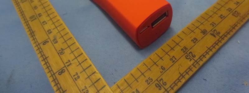
AAO2302500
Feb 10, 2015Bluetooth Power Bank
Equipment Class
DXX - Part 15 Low Power Communication Device Transmitter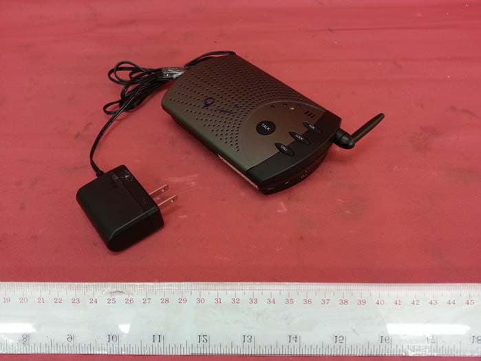
AAO4300124C
May 02, 2013900MHz Wireless Intercom
Equipment Class
DXT - Part 15 Low Power Transceiver, Rx Verified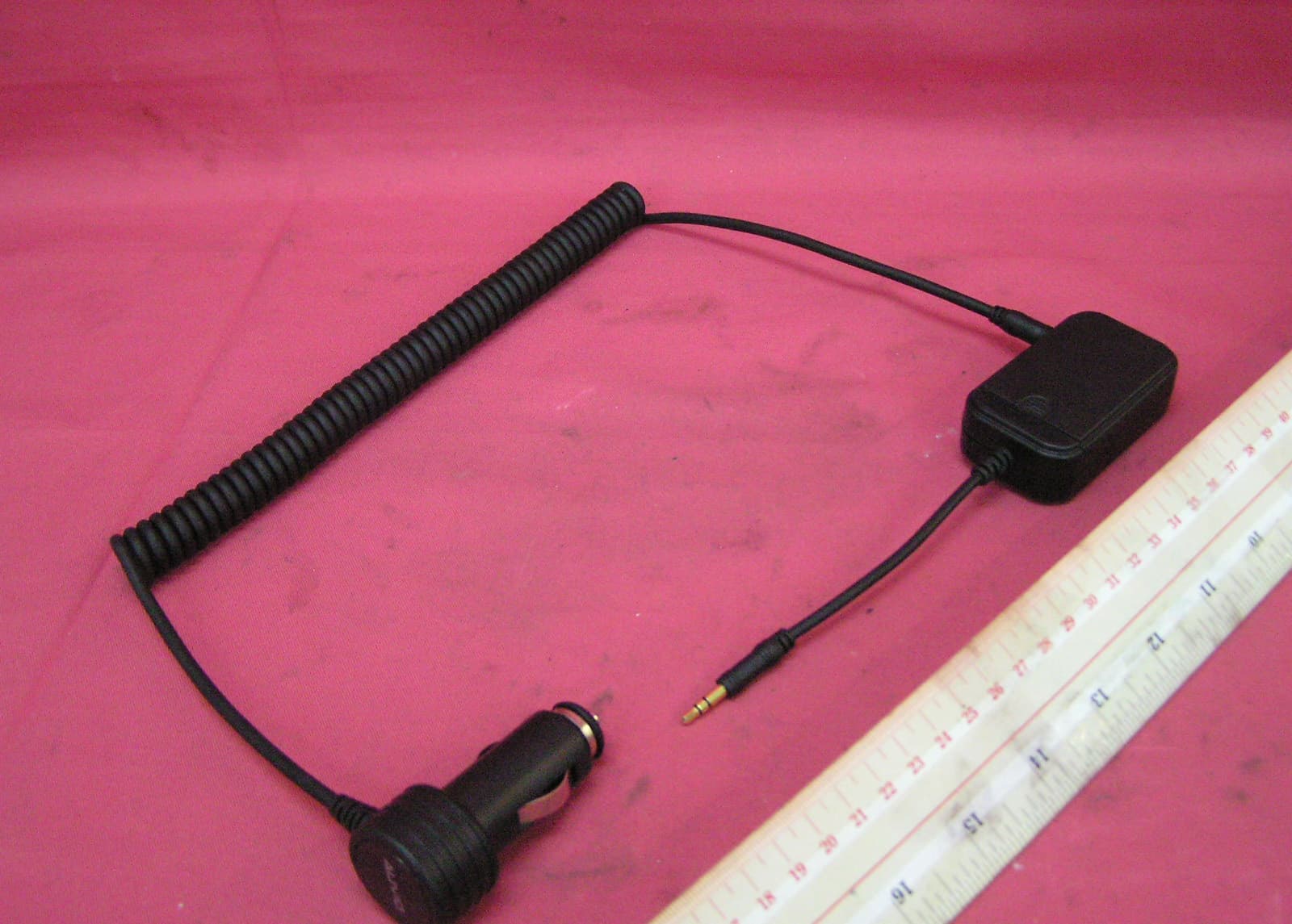
AAO1200876
Nov 30, 2011Universal FM Transmitter
Equipment Class
DXX - Part 15 Low Power Communication Device Transmitter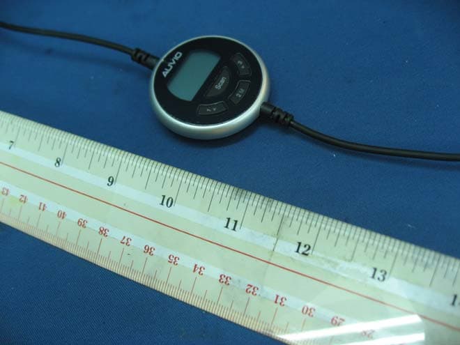
AAO1200962
Aug 02, 2011Universal FM Transmitter
Equipment Class
DXX - Part 15 Low Power Communication Device Transmitter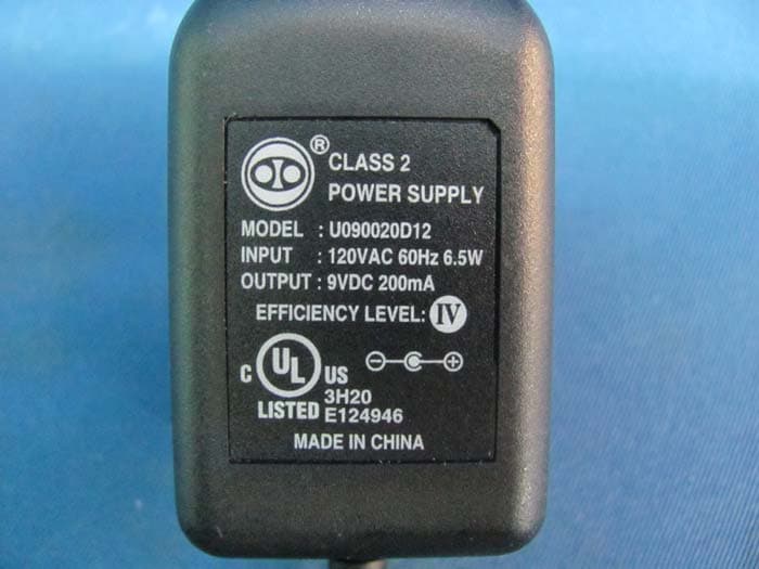
AAO1500044T
Apr 02, 20112.4GHz Digital Wireless Rear Speaker Kit - Transmitter
Equipment Class
DSS - Part 15 Spread Spectrum Transmitter