AAO3301253T2.4GHz FHSS Wireless Headphone (Base)
RadioShack Corporation
Click to zoom
Application Details
- Equipment Class
- DSS - Part 15 Spread Spectrum Transmitter
- Date of Grant
- Jan 05, 2006
- Application Purpose
- Original Equipment
- Date of Application
- Jan 05, 2006
- Equipment Note
- 2.4GHz FHSS Wireless Headphone (Base)
- Frequency Range
- 2404.32000000 - 2476.35000000
- Company
- RadioShack Corporation
- Country
- United States
Documents & Files
Document Text
Text extracted from the exhibit documents filed with the FCC. Open a document above to read the original.
Users Manual
Please read this user’s guide before installing, setting up and using your new product www.radioshack.com 33-1253 2.4GHz Wireless Headphones Thank you for purchasing your 2.4GHz Wireless Headphones from RadioShack. Your headphones let you comfortably enjoy your music with greater mobility than wired headphones. 2.4GHz Wireless Headphones Universal Dongle 1-to-2 Charging Hub AC adapter User’s Guide what’s included ©2005 RadioShack Corporation. All rights reserved. RadioShack and RadioShack.com are trademarks used by RadioShack Corporation. AO0256AAA1 33-1253 12A05 Printed in China To protect your hearing, follow these guidelines when you use headphones: • Do not listen at extremely high volume levels. Extended high-volume listening can lead to permanent hearing loss. • Set the volume to the lowest setting before you begin listening. Then, adjust the volume to a comfortable level. After you set the volume, do not increase it. • Do not wear headphones while operating a motor vehicle or riding a bicycle. This can create a traffic hazard and is illegal in some areas. listening and traffic safety Your headphones and dongle are each powered by a built-in NiMH rechargeable battery, which you can charge with the supplied 1-to-2 charging hub. • The LED on the charging hub lights amber during charging and changes to green when the headphones and dongle are fully charged. • To optimize rechargeable battery life, discharge all power in the batteries before recharging your headphones and dongle. charging the headphones and dongle • Keep your headphones within 32 feet (about 10 meters) within sight of the dongle. To avoid interference, use only one set of headphones within the active dongle’s operating range. • If the headphone or dongle LED do not light up when turned on, recharge the batteries. • Use only one headphone with one dongle. using the headphones Operating Frequency ..................................2.4GHz Operating Range ................................up to 32 feet Headphones Playtime ..................... about 7 hours Frequency Response (6dB) .............. 80Hz – 20KHz Audio S/N .......................................................70dB Audio Resolution ...........................................16 bit Audio Sample Rate .................................. 44.1KHz Charging Time(dongle and headphone) ... 4 hours Specifications are typical; individual units might vary. Specifications are subject to change and improvement without notice. Actual product may vary from the images found in this document. specifications This equipment has been tested and found to comply with the limits for a Class B digital device, pursuant to Part 15 of the FCC Rules. These limits are designed to provide reasonable protection against harmful interference in a residential installation. This equipment generates, uses, and can radiate radio frequency energy and, if not installed and used in accordance with the instructions, may cause harmful interference to radio communications. However, there is no guarantee that interference will not occur in a particular installation. If this equipment does cause harmful interference to radio or television reception, which can be determined by turning the equipment off and on, the user is encouraged to try to correct the interference by one or more of the following measures: • Reorient or relocate the receiving antenna. • Increase the separation between the equipment and receiver. • Consult your local RadioShack store or an experienced radio/TV technician for help. • If you cannot eliminate the interference, the FCC requires you to stop using the headphones. Changes or modifications not expressly approved by RadioShack may cause interference and void the user’s authority to operate the equipment. This device complies with Part 15 of the FCC Rules. Operation is subject to the following two conditions: (1) this device may not cause harmful interference, and (2) this device must accept any interference received, including interference that may cause undesired operation. RF Emissions Information This product is warranted by RadioShack against manufacturing defects in material and workmanship under normal use for ninety (90) days from the date of purchase from RadioShack company-owned stores and authorized RadioShack franchisees and dealers. For complete warranty details and exclusions, check with your local RadioShack store. RadioShack Customer Relations 300 RadioShack Circle, Fort Worth, TX 76102 04/04 limited 90-day warranty Power Switch LED NOTES NOTES Volume Headphones LED Indicator Dongle 1-to-2 Charging Hub AC Adapter 1. Plug the AC adapter’s barrel plug into the charging hub. 2. Plug the two charging hub barrel plugs into the headphones and dongle. 3. Connect the AC adapter to an AC outlet. 1. Connect the dongle to the audio output jack of an audio source, and slide the dongle power switch forward. The green LED will light. 2. Slide the headphones power switch forward. The green LED will light. 3. Place the headphone ear hooks over your ears with the connecting band behind your neck. 4. Play your music, and adjust your headphone volume. Audio Source LED Indicator Power Switch Ear Hooks 33-1253.120105.indd 112/02/2005 9:57:45 AM
Block Diagram
Block Diagram FCC ID: AAO3301253T FCC ID: AAO3301253T FCC ID: AAO3301253T RF Block Diagram IF = 6MHz BW = 4MHz VCO: Tx: 2404 to 2476 MHz VCO: Rx: 2410 to 2482 MHz
External Photos
External photos FCC ID: AAO3301253T External photos FCC ID: AAO3301253T External photos FCC ID: AAO3301253T
ID Label/Location Info
FCC ID: AAO3301253T Label Location Scale: 1:1 ~ 15 x 3 mm
Internal Photos
Internal photos FCC ID: AAO3301253T Internal photos FCC ID: AAO3301253T Internal photos FCC ID: AAO3301253T
Operational Description
33-1253 Technical description: Introduction: The 33-1253 consists of a 2.4GHz dongle and a 2.4GHz headphone. Any analog music source that is applied to the dongle will be sent to the headphone via 2.4GHz RF link without any compression. The audio being sent by the dongle will be reproduced at the headphone side. Dongle operation: The role of the dongle is to accept any analog audio input and transmit the audio data to the corresponding headphone. ADC: The audio encoding is done by the ADC chip uDA1361TS (U4). The uDA1361TS is a single chip stereo analog-to-digital converter employing bit-stream conversion techniques. The ADC chip is set to master mode and system clock apply to the chip is about 11.29MHz (fsys). Therefore the sampling frequency is 44.1KHz (fsys/256) and with a resolution of 16 bit digital data. 2.4GHz wireless audio streamer: The digital data will then be sent to the 2.4GHz wireless audio streamer chip nRF24Z1 (U1). U1 works as an 2.4GHz RF transceiver with 4MBit/S data rate. It handles audio I/O, RF protocol and RF link management. The EEPROM chip (U2) stores the initial configuration of the U1. Once the unit is powered on, U1 goes into a power on reset, and the reset is held until the supply voltage is kept higher than the minimum operation voltage (2V) for a few millisecond. When the reset is released, the chip needs to be configured. It will look for the external EEPROM (U2) memory on the SPI master interface. Then configuration data is load from U2. Once U1 is configured, it starts the link-locate state that the dongle will try to establish link with the corresponding headphone by iteratively sending short search packages on all available channels until acknowledge is received from the corresponding headphone. Once the acknowledge is received, the dongle will enter the synchronization state. This synchronization state takes care of synchronizing the channel hopping engine on dongle and headphone, to secure that both parts follows the same hopping sequence. Which channel to start from is implicitly found during the link-locate state. When the dongle and headphone are in synchronization mode, the audio stream formats are converted to the nRF24Z1 RF protocol and transferred over the air. Power step up: The operation voltage is kept at 2.5V by a step up chip XC6371C251PR (U6) that is supplied by battery voltage. FCC ID: AAO3301253T Low battery: The battery monitor chip XC61CN2002MR/BU4820 (U9) that connects its input to the battery, works as a 2V battery monitor chip. When the battery voltage drops below 2V, it’s output will be dropped from Vdd (2.5V) to zero volt. Then the ADC chip (U4) is powered down and the LED (D3) will also be turned off. Battery charging for both dongle and headphone: Once the charging hub (provided) is connected to the power jack of either the dongle or the headphone. The battery voltage is disconnected from the main circuit and therefore the unit can not be operated when it is charging. FCC ID: AAO3301253T 32-1253 uses a single chip transceiver IC from Nordic nRF24Z1. RF PART The single chip transceiver IC contains all necessary RF circuit. It converts the RF FSK signal picked up by the antenna for further processing. Besides, the base band digital signal, including voice and commands, will be modulated to FSK format on the RF carrier during transmission. The main building blocks of the RF parts includes a LNA, Mixer, IF Band pass filter, VCO with frequency synthesiser, RF power amplifier for transmission. Among those building blocks, the RF circuit can be divided into two sections. A: RX section This product employs traditional single conversion architecture with the following functional blocks: 1. The LNA has low noise figure and high insertion gain. 2. The LO signal is generated VCO and the LO frequency is controlled by the frequency synthesizer after received command from external MCU. 3. The mixer is to convert RF signal to an IF signal. This IF signal will further filter by the IF band pass filter. 4. The IF signal is then down converted to digital signals, i.e. CLK and DATA. 5. The digital DATA is further convert to analogue voice signal through the external DAC IC. B: TX section 1. The digital DATA is from the external ADC and it is applied to the transceiver IC. 2. It is further filtered by the GFSK filter before going to the VCO and the frequency of transmission is controlled by the frequency synthesizer. 3. The FSK modulated signal is amplified by the internal PA. 4. The amplified RF signal is applied to the antenna with the external matching circuit. FCC ID: AAO3301253T
Operational Description
PRELIMINARY PRODUCT SPECIFICATION Main office: Nordic Semiconductor ASA - Vestre Rosten 81, N-7075 Tiller, Norway - Phone +4772898900 - Fax +4772898989 Revision: 2.1 Page 1 of 80 July 2005 2.4GHz wireless audio streamer FEATURES APPLICATIONS • Low cost 0.18u CMOS process, 36 pin 6x6mm QFN package • Compact Disk, CD quality headset • Single chip 2.4GHz RF transceiver • MP3 / Mini Disk headset • 4Mbit/sec RF link • Speakers • Input sample rate up to 96kHz, 24 bits • Surround speakers • Output sample rate up to 48kHz, 24 bits • Microphone • Programmable latency • Musical instruments • Quality of Service engine supporting up to 1.536 Mbit/s LPCM audio • Audio streaming from PC soundcard to HiFi system • S/PDIF interface for direct connection to PC soundcard and surround receivers • Download MP3 files from PC to MP3 player • I2S interface for glue-less audio support • Compressed video streaming • SPI or 2-wire interface for up to 12 kbit/sec peak bi- directional digital control/AUX data • On chip optional compression • On chip voltage regulators • Few external components • Uses global 2.4GHz band GENERAL DESCRIPTION nRF24Z1 provides a true single chip system for CD quality audio streaming of up to16 bit 48 kHz audio with support of up to 24 bit 96 kHz input. I2S and S/PDIF interfaces are supported for audio I/O. Seamless interfacing of low cost A/D and D/A for analog audio input and output. SPI or 2-wire (I2C compatible) serial interfaces for control. The circuit has embedded voltage regulators, giving maximum noise immunity and operation from a single 2.0V to 3.6V supply. QUICK REFERENCE DATA Parameter Value Unit Minimum supply voltage 2.0 V Temperature range -20 to +80 °C Peak supply current in transmit @ -5dBm output power 15 mA Peak supply current in receive mode 32 mA Supply current in power down mode 4 μA Maximum transmit output power 0 dBm Audio sample rate 8 to 96 kS/s Audio resolution 16 bit Receiver sensitivity -80 dBm Table 1-1 nRF24Z1 quick reference data. nRF24Z1 PRELIMINARY PRODUCT SPECIFICATION nRF24Z1 wireless audio streamer Main office: Nordic Semiconductor ASA - Vestre Rosten 81, N-7075 Tiller, Norway - Phone +4772898900 - Fax +4772898989 Revision: 2.1 Page 2 of 80 July 2005 ORDERING INFORMATION Type number Description Version nRF24Z1 36L QFN 6x6 mm B nRF24Z1-EVKIT Evaluation kit 1.0 Table 1-2 nRF24Z1 ordering information. PRELIMINARY PRODUCT SPECIFICATION nRF24Z1 wireless audio streamer Main office: Nordic Semiconductor ASA - Vestre Rosten 81, N-7075 Tiller, Norway - Phone +4772898900 - Fax +4772898989 Revision: 2.1 Page 3 of 80 July 2005 TABLE OF CONTENTS FEATURES ............................................................................................................................1 APPLICATIONS ....................................................................................................................1 GENERAL DESCRIPTION ...................................................................................................1 QUICK REFERENCE DATA ................................................................................................1 ORDERING INFORMATION ...............................................................................................2 TABLE OF CONTENTS........................................................................................................3 1 Pin Assignment ...............................................................................................................6 2 Pin Function ....................................................................................................................7 3 Glossary of terms ............................................................................................................8 4 Architectural Overview...................................................................................................9 4.1 Audio transmitter ..................................................................................................11 4.1.1 I2S audio input ..............................................................................................11 4.1.2 S/PDIF audio input .......................................................................................12 4.1.3 Serial control (slave) interfaces ....................................................................12 4.1.4 Master interfaces ...........................................................................................12 4.1.5 Direct data input pins ....................................................................................13 4.1.6 Interrupt output .............................................................................................13 4.2 Audio Receiver .....................................................................................................13 4.2.1 I2S audio output ............................................................................................14 4.2.2 S/PDIF audio output .....................................................................................15 4.2.3 Master interfaces ...........................................................................................15 4.2.4 Serial control (slave) interfaces ....................................................................15 4.2.5 Parallel port and PWM..................................................................................15 4.3 Blocks common to audio transmitter and receiver ...............................................16 4.3.1 XTAL Oscillator ...........................................................................................16 4.3.2 Radio Transceiver .........................................................................................16 4.3.3 Quality of Service (QoS) engine...................................................................16 4.3.4 Audio compression / decompression ............................................................17 4.3.5 Power .............................................…
Text truncated - open the document above for the full version.
Operational Description
33-1253 Designated frequency hopping algorithm: Pseudorandom Frequency Hopping Sequence Describe how the hopping sequence is generated. Provide an example of the hopping sequence channels, in order to demonstrate that the sequence meets the requirement specified in the definition of a frequency hopping spread spectrum system. The frequency hopping is implemented in 18 non-overlap channels. The hopping is sequentially after the contents of the frequency hopping table CH01, CH08, CH14.... CH11, CH17, CH06 and so on. The example of the hopping sequence channels table shown below. Hopping table. (Total 18 channel frequencies in each sequences) Channel Table Sequence 1 Sequence 2 Channel 01 2404.320 MHz Channel 01 2404.320MHz Channel 07 2428.310 MHz Channel 02 2408.300 MHz Channel 08 2432.310MHz Channel 16 2468.320 MHz Channel 03 2412.310 MHz Channel 14 2460.330MHz Channel 08 2432.310 MHz Channel 04 2416.290 MHz Channel 03 2412.310MHz Channel 17 2472.350 MHz Channel 05 2420.330 MHz Channel 10 2440.310MHz Channel 09 2436.330 MHz Channel 06 2424.310 MHz Channel 16 2468.320MHz Channel 18 2476.350 MHz Channel 07 2428.310 MHz Channel 05 2420.330MHz Channel 10 2440.310 MHz Channel 08 2432.310 MHz Channel 12 2448.320MHz Channel 01 2404.320 MHz Channel 09 2436.330 MHz Channel 18 2476.350MHz Channel 11 2444.320 MHz Channel 10 2440.310 MHz Channel 07 2428.310MHz Channel 02 2408.300 MHz Channel 11 2444.320 MHz Channel 13 2456.310MHz Channel 12 2448.320 MHz Channel 12 2448.320 MHz Channel 02 2408.300MHz Channel 03 2412.310 MHz Channel 13 2456.310 MHz Channel 09 2436.330MHz Channel 04 2416.290 MHz Channel 14 2460.330 MHz Channel 15 2464.340MHz Channel 13 2456.310 MHz Channel 15 2464.340 MHz Channel 04 2416.290MHz Channel 05 2420.330 MHz Channel 16 2468.320 MHz Channel 11 2444.320MHz Channel 14 2460.330 MHz Channel 17 2472.350 MHz Channel 17 2472.350MHz Channel 06 2424.310 MHz Channel 18 2476.350 MHz Channel 062424.310MHz Channel 15 2464.340 MHz The sequences are generated by Matlab RAND function in which calculate uniformly distributed random numbers. The first 18 channels are grouped into Sequence 1. Sequence 2 is generated by the same function with only the same 18 channels are selected (in different order). Equal Hopping Frequency Use Describe how each individual EUT meets the requirement that each of its hopping channels is used equally on average (e.g., that each new transmission event begins on the next channel in the hopping sequence after the final channel used in the previous transmission event). In a clean RF environment, which means few or no other RF transmitters nearby, the nRF24Z1 will use all the channels in hopping table. FCC ID: AAO3301253T 1 A synchronized frequency hopping table is kept in the ARX by use of the service channel superimposed on the audio stream. In summary: All channels will on average be used equally. Thop depends on the audio rate, you can find values below: Fs=44.1kHz : Thop=2.9ms System Receiver Input Bandwidth Describe how the associated receiver(s) complies with the requirement that its input bandwidth (either RF or IF) matches the bandwidth of the transmitted signal. It's the same RF device, the only difference is that one is set as a transmitter and the other in receive mode. Main data stream is one-way audio, which is why they are referred to as a transmitter and receiver. The receiver bandwidth is 4000kHz where the 20dB bandwidth of transmitter is 2450kHz. System Receiver Hopping Capability Describe how the associated receiver(s) has the ability to shift frequencies in synchronization with the transmitted signals. A two-way low speed data and control channel makes it possible to exchange information. The ARX will start every frame with a ACK on new channel, the ACK will also contain the next 8 channels to use in the hopping scheme. This way even if a ACK is lost, both devices will know which channels to use next. Section 15.247(h) Describe how the EUT complies with the requirement that it not have the ability to be coordinated with other FHSS systems in an effort to avoid the simultaneous occupancy of individual hopping frequencies by multiple transmitters Since the banning list was disabled. So our device does not have the ability to be coordinated with other FHSS systems in an effort to avoid the simultaneous occupancy of individual hopping frequencies by multiple transmitters. Moreover, our device has a unique user ID for link registration. So no other FHSS system can join the link with our device. FCC ID: AAO3301253T 2 FCC ID: AAO3301253T 3 Data frame structure: Each ATX frame consist of 8 packets. Each packets will have - 1 byte preamble - 9 bytes address and control data - 64 bytes audio data - 2 bytes CRC Each ARX acknowledge packet consist of - 1 byte preamble - 27 bytes address and control data - 2 bytes CRC All bits are "ON" in the worst case for both ATX and ARX. ATX 1. The maximum transmitting time is 1.32ms and it is fixed. 2. One frame in each hop and carry a fixed number of frame. ARX 1. The maximum transmitting time is 164us and it is fixed. 2. One frame in each hop and carry a fixed number of frame. Remarks Only one frame will be transmitted in each hop and the hopping time is 2.9ms which is mentioned as above. The transmitter (dongle unit) will waiting the acknowledge packet from the receiver (headphone unit) after the frame transmitted.
RF Exposure Info
INTERTEK TESTING SERVICES FCC ID: AAO3301253T RF exposure For Specific Absorption Rate (SAR) evaluation of the transmitter, with reference to TCB Exclusions List revised on July 17, 2002, portable transmitters with output power less than low threshold and operating within 2.5cm from person’s body can be certified by TCB without the SAR evaluation. The output power for portable transmitters is defined as the higher of the conducted or radiated (EIRP) source- based time averaging output power. And the low threshold is equal to (60/f GHz ) mW for d < 2.5cm, where f GHz is mid-band frequency in GHz, and d is the distance from the portable transmitter to a person’s body, excluding hands, wrists, feet, and ankles. For the transmitter of the tested model of 33-1253, the measured peak conducted power was 1.28 mW. The maximum source-based time averaging duty factor in 45.5172%. The conducted source-based time averaging output power = (1.28 * 0.45517) mW = 0.58262 mW The measured maximum field strength (FS) was 103.2 dBμV/m. The distance (D) between the antenna and the equipment under test (EUT) was 3 meters. From these data, the radiated (EIRP) source-based time-averaging output power can be calculated by: The radiated power = (FS*D) 2 / 30 mW = 6.2679 mW The radiated (EIRP) source-based time-averaging output power = (6.2679 * 0.45517) mW = 2.85296 mW The low threshold in the 2400-2483.5 band is 24.57 mW. From the above calculation, output power obtained in both method is less than low threshold, it is concluded that the transmitter can be certified by TCB without the SAR evaluation.
Test Report
• The test results reported in this test report shall refer only to the sample actually tested and shall not refer or be deemed to refer to bulk from which such a sample may be said to have been obtained. • This report shall not be reproduced except in full without prior authorization from Intertek Testing Services Hong Kong Limited. • For Terms And Conditions of the services, it can be provided upon request. • The evaluation data of the report will be kept for 3 years from the date of issuance. Intertek Testing Services Hong Kong Ltd. 2/F., Garment Centre, 576 Castle Peak Road, Kowloon, Hong Kong. Tel: (852) 2173 8888 Fax: (852) 2741 1693 Website: www.hk.intertek-etlsemko.com RadioShack Corporation Application For Certification 2.4GHz Digital Wireless Headphone Transmitter (FCC ID: AAO3301253T) 05205161 TC/el November 30, 2005 INTERTEK TESTING SERVICES FCC ID: AAO3301253T i LIST OF EXHIBITS INTRODUCTION EXHIBIT 1: Summary of Tests EXHIBIT 2: General Description EXHIBIT 3: System Test Configuration EXHIBIT 4: Measurement Results EXHIBIT 5: Equipment Photographs EXHIBIT 6: Product Labelling EXHIBIT 7: Technical Specifications EXHIBIT 8: Instruction Manual INTERTEK TESTING SERVICES FCC ID: AAO3301253T ii MEASUREMENT/TECHNICAL REPORT RadioShack Corporation - MODEL: 33-1253 FCC ID: AAO3301253T This report concerns (check one:) Original Grant X Class II Change Equipment Type: DSS-Part 15 Spread Spectrum Transmitter Deferred grant requested per 47 CFR 0.457(d)(1)(ii)? Yes No X If yes, defer until: date Company Name agrees to notify the Commission by: date of the intended date of announcement of the product so that the grant can be issued on that date. Transition Rules Request per 15.37? Yes No X If no, assumed Part 15, Subpart C for intentional radiator − the new 47 CFR [10-01-04 Edition] provision. Report prepared by: Alfred Lo Intertek Testing Services 2/F., Garment Center, 576 Castle Peak Road, Kowloon, Hong Kong. Phone: 852-2173-8545 Fax: 852-2371-0914 INTERTEK TESTING SERVICES FCC ID: AAO3301253T iii Table of Contents 1.0 Summary of Test ..................................................................................................... 2 2.0 General Descripton ................................................................................................. 4 2.1 Product Description .......................................................................................... 4 2.2 Related Submittal(s) Grants.............................................................................. 5 2.3 Test Methodology ............................................................................................. 5 2.4 Test Facility ...................................................................................................... 5 3.0 System Test Configuration..................................................................................... 7 3.1 Justification....................................................................................................... 7 3.2 EUT Exercising Software .................................................................................. 7 3.3 Support Equipment List and Description ........................................................... 8 3.4 Measurement Uncertainty................................................................................. 9 3.5 Equipment Modification .................................................................................... 9 4.0 Measurement Results........................................................................................... 11 4.1 Maximum Conducted Output Power at Antenna Terminals ............................ 11 4.2 Maximum 20dB RF Bandwidth ....................................................................... 12 4.3 Minimum Number of Hopping Frequencies..................................................... 13 4.4 Minimum Hopping channel Carrier Frequency Separation.............................. 14 4.5 Average Channel Occupancy Time ................................................................ 15 4.6 Out of Band Conducted Emissions ................................................................. 16 4.7 Out of Band Radiated Emissions .................................................................... 17 4.8 Transmitter Radiated Emissions in Restricted Bands ..................................... 18 4.9 Field Strength Calculation............................................................................... 19 4.10 Radiated Emission Configuration Photograph - Transmitter Unit .................... 20 4.11 Radiated Emission Data - Transmitter Unit ..................................................... 21 4.12 AC Line Conducted Emission ......................................................................... 25 4.13 Line Conducted Configuration Photograph ..................................................... 26 4.14 Line Conducted Emission ............................................................................... 27 4.15 Radiated Emissions from Digital Section of Transceiver ................................. 28 4.16 Transmitter Duty Cycle Calculation and Measurements ................................. 30 5.0 Equipment Photographs ....................................................................................... 32 6.0 Product Labelling .................................................................................................. 34 7.0 Technical Specifications ....................................................................................... 36 8.0 Instruction Manual................................................................................................ 38 INTERTEK TESTING SERVICES FCC ID: AAO3301253T iv List of Attached File Exhibit Type File Description Filename Test Report Test Report report.pdf Test Report Maximum Output Power Plot bmaxop.pdf Test Report 20dB Bandwidth Plot b20dB.pdf Test Report Minimum Number of Hopping Frequencies bchno.pdf Test Report Minimum Hopping Channel C…
Text truncated - open the document above for the full version.
Test Report
Report No.: 0520516 Charging mode AC Mains Ctrl No.: PAGE 1 Tested By:Hong, Report No.:0520516 Scan Settings (1 Range) |--------- Frequencies -----------||----------- Receiver Settings ------------| Start Stop Step IF BW Detector M-Time Atten Preamp OpRge 150k 30M 5k 10k PK+AV 10ms AUTO LN OFF 60dB Final Measurement: x QP / + AV Meas Time: 1 s Subranges: 16 Acc Margin: 20dB Transducer No. Start Stop Name 1 15 9k 30M EW0090 21 9k 30M EW0698 0 10 20 30 40 50 60 70 80 90 dBuV 100 0.15 MHz 30 110 F15Q F15A Report No.: 0520516 Charging mode AC Mains Ctrl No.: Tested By:Hong, Report No.:0520516 Scan Settings (1 Range) |--------- Frequencies -----------||----------- Receiver Settings ------------| Start Stop Step IF BW Detector M-Time…
Text truncated - open the document above for the full version.
Contact Information
Applicant
Elizabeth Granados(Regulatory Affairs Manager)
Technical Contact
Intertek Testing Services Hong Kong Ltd.Alfred Lo
[email protected]852-2173-8545
2/F., Garment Centre, · Kowloon · Hong Kong
Non-Technical Contact
Intertek Testing Services Hong Kong Ltd.Alfred Lo
[email protected]852-2173-8545
Test Firm
Intertek Testing Services Hong KongBilly Chow
Technical Specifications
| # | Rule Parts | Frequency Range | Power Output |
|---|---|---|---|
| 1 | 15C | 2.40 GHz - 2.48 GHz | 1.28 mW |
Other Applications from RadioShack Corporation
AAO2302500
Feb 10, 2015Bluetooth Power Bank
Equipment Class
DXX - Part 15 Low Power Communication Device Transmitter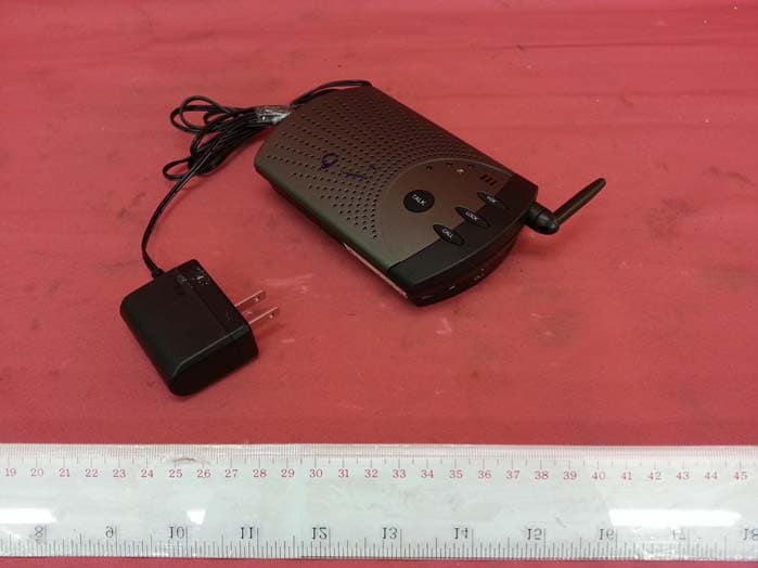
AAO4300124C
May 02, 2013900MHz Wireless Intercom
Equipment Class
DXT - Part 15 Low Power Transceiver, Rx Verified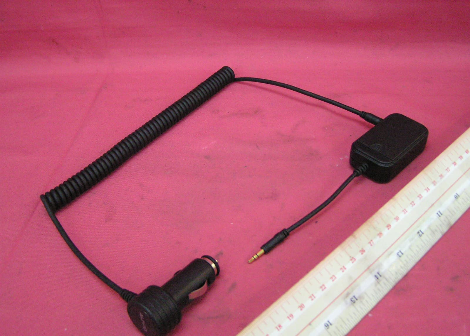
AAO1200876
Nov 30, 2011Universal FM Transmitter
Equipment Class
DXX - Part 15 Low Power Communication Device Transmitter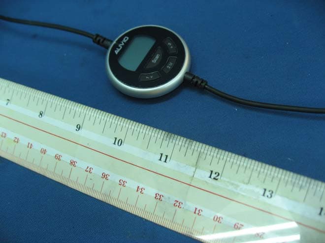
AAO1200962
Aug 02, 2011Universal FM Transmitter
Equipment Class
DXX - Part 15 Low Power Communication Device Transmitter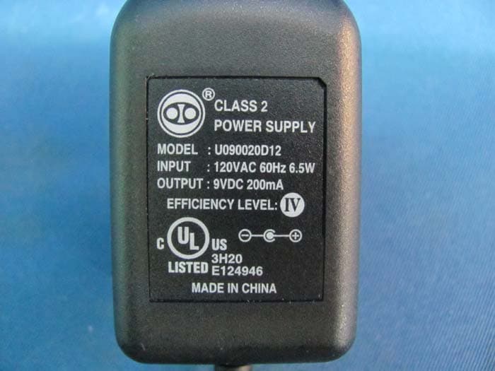
AAO1500044T
Apr 02, 20112.4GHz Digital Wireless Rear Speaker Kit - Transmitter
Equipment Class
DSS - Part 15 Spread Spectrum Transmitter