ACEC4205B2.4GHz 20 Channel Cordless Phone
Clarity, A Division of Plantronics, Inc.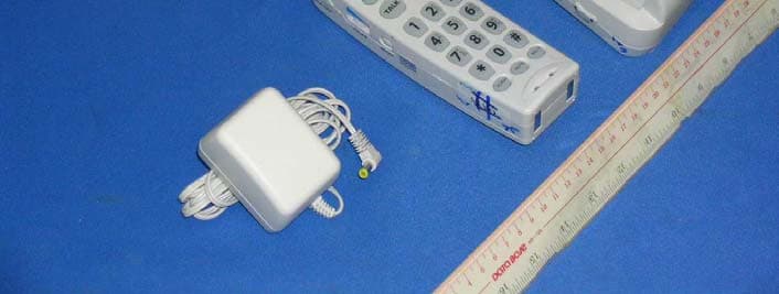
Click to zoom
Application Details
- Equipment Class
- DXT - Part 15 Low Power Transceiver, Rx Verified
- Date of Grant
- Aug 30, 2006
- Application Purpose
- Original Equipment
- Date of Application
- Aug 30, 2006
- Equipment Note
- 2.4GHz 20 Channel Cordless Phone
- Frequency Range
- 2481.55000000 - 2482.50000000
- Country
- United States
Documents & Files
Document Text
Text extracted from the exhibit documents filed with the FCC. Open a document above to read the original.
Block Diagram
Revision 02.02 RF Module (Base) Block Diagram Revision 02.02 RF Module (Handset) Block Diagram
External Photos
INTERTEK TESTING SERVICES External Photos FCC ID: ACEC4205B external photos - 1 of 2 INTERTEK TESTING SERVICES External Photos FCC ID: ACEC4205B external photos - 2 of 2
ID Label/Location Info
C4205 Rev.6 06/22/2006 IC:1186C-C4205 FCC ID:ACEC4205B Model: C4205 19 x 7.5mm 16 x 10mm 9V DC 400 mA TEL ( ) 2 10.7mm 55 x 40mm 70255
Internal Photos
INTERTEK TESTING SERVICES Internal photos FCC ID: ACEC4205B internal photos - 1 of 10 Base Unit assembly Base Unit Main PCB comp side (View 1) INTERTEK TESTING SERVICES Internal photos FCC ID: ACEC4205B internal photos - 2 of 10 Base Unit Main PCB comp side (View 2) Base Unit Main PCB comp side (View 3) INTERTEK TESTING SERVICES Internal photos FCC ID: ACEC4205B internal photos - 3 of 10 Base Unit Main PCB solder side Base Unit Telephone and AC Jack front side INTERTEK TESTING SERVICES Internal photos FCC ID: ACEC4205B internal photos - 4 of 10 Base Unit Telephone and AC Jack rear side Base Unit Ringer LED front side INTERTEK TESTING SERVICES Internal photos FCC ID: ACEC4205B internal photos - 5 of 10 Base Unit Ringer LED rear side Base Unit Charge and Control front side INTERTEK TESTING SERVICES Internal photos FCC ID: ACEC4205B internal photos - 6 of 10 Base Unit Charge and Control rear side Base Unit Oscillator PCB comp side INTERTEK TESTING SERVICES Internal photos FCC ID: ACEC4205B internal photos - 7 of 10 Base Unit Oscillator PCB solder side INTERTEK TESTING SERVICES Internal photos FCC ID: ACEC4205B internal photos - 8 of 10 Handset assembly Handset Main PCB comp side (View 1) INTERTEK TESTING SERVICES Internal photos FCC ID: ACEC4205B internal photos - 9 of 10 Handset Main PCB comp side (View 2) Handset Main PCB Keypad side INTERTEK TESTING SERVICES Internal photos FCC ID: ACEC4205B internal photos - 10 of 10 Handset Oscillator PCB comp side Handset Oscillator PCB solder side
Operational Description
C4205 Circuit Description CONTENT 1. Introduction 2. Functional Blocks of the Handset 3. Handset Unit Circuit Block Description 4. Functional Blocks of the Base unit 5. Base Unit Circuit Block Description 6. Functional Blocks of the RF Module 7. RF Module Circuit Block Description 8. C4205 Basic Operation 9. Test Mode Operation 10. RF Channels Revision 02.02 1. Introduction The model C4205 is a 20 channel (2.4GHz) cordless telephone. This unit is made up of two parts: a. A Handset unit. b. A Base unit. A security code of over 65,000 different combinations is used to prevent access by a different phone on a different line. This code is randomly and automatically changed each time the handset is placed in the cradle. 2. Functional Blocks of the Handset The block diagram of C4205 handset unit is as shown below. It is made up of the following parts: 2.1 Keyboard Matrix, Switches and Function LED 2.2 MCU and MCU Interface 2.3 RF Module 2.4 Compander 2.5 Data Shaper 2.6 Charge and Control 2.7 Low Battery Detector 2.8 Buzzer 2.9 Audio Circuit Revision 02.02 3.1 Keyboard Matrix, Switches and Function LED The keyboard consists of the following keys: • FIRE – one touch memory key • POL – one touch memory key • AMB – one touch memory key • CHN – for changing RF carrier frequency • TALK – for On/Off hook control • MEM – for memory program and dialing • 1, 2, 3, 4, 5, 6, 7, 8, 9, *, 0, # – numeric keys • FLASH – provides timed On/Off hook function • RDL/P – redials the last number or provides a pause during dialing. The keyboard is connected to Pins 19 to 20, 22 to 26 and 30 of the MCU (U1). • MUTE – turns Off/On the handset microphone The MUTE key is connected to the DSP_MODULE board. The switches consist of the followings: • BOOST CLARITY POWER – for On/Off the receiver amplifier gain. This is connected to the DSP_MODULE board. • RINGER ON/VIBRATOR/OFF – turns On/Off the ringer buzzer and the vibrator. This is connected to pins 21 and 38 of MCU. The function LEDs consist of the followings: • MICMUTE (LED317 - Red) – Located under the “MUTE” key. On/Off when microphone is Off/On • INUSE (LED316 – Green; LED301 - Red) – Located under the “TALK” key and the handset antenna. On/Off when telephone is Off-hook/On-hook • BOOST (LED316 – RED) – Located under the “TALK” key. On/Off when the receiver amplifier extra gain is On/Off • BACKLIGHT (LED304 – LED315 – Orange) – Located under the keyboard. On for a short time when any key is pressed • RINGER (LED301 - Red) – Located in the handset antenna. Flashes when the telephone line rings These LEDs are controlled by pins 9, 11, 12 of MCU and the DSP_MODULE board. Revision 02.02 3.2 MCU and MCU Interface The controller of the handset is U1. The frequency of the crystal used is 4.09 MHz. It controls the functions of the handset through the keyboard interface and signals from the base unit. The data to and from the base goes through pin 31 (data from base) and pin 34 (data to base). 3.3 RF Module For operation and frequency see RF module section. It receives the PLL data through RFM1 pins 4, 5, 6 from MCU pins 44, 43, and 1. The antenna located at the top of the unit and is permanent attached to RF module through a copper wire. 3.4 Compander A compander U201 is used for improving the S/N of transmit and receive audio signals. 3.5 Data Shaper The information which sent from base unit is recovered by the amplifier Q201 and Q202. 3.6 Charge and Control ZD201, Q207, D212, D213, D214, D215, D218, D219 provide polarity and over-voltage protection during battery charging. The charge signal is detected by pin 29 of the MCU. When the handset is put into the base cradle, a negative pulse is sent to pin 14 of the MCU. 3.7 Low Battery Detector The battery voltage is detected by U6B and Q1. The signal is sent to pin 4 of MCU. 3.8 Buzzer and Vibrator Q204 is the buzzer signal amplifier and driven by the MCU pins 2, 32, 33. Q301 is the switch to turn on the vibrator. It receives its control signal from pin 39 of the MCU. 3.9 Audio Circuit Revision 02.02 Speech signal is picked up by the internal microphone MIC1 and sent to the gain control module U8 (DSP_MODULE) and sent to telephone line through the compander U201 and the RF module. The incoming speech is received through the RF module, the compander, the gain control module U8 (DSP_MODULE) and amplifier U2. When BOOST is On, extra gain is inserted in this audio path. The headset jack is for external speaker and microphone. The neckloop jack is for an external hearing aid device. U7 provides regulated +3.0V for U8 and is controlled by U1 pin 41. The power to the power amplifier U2 is supplied by Q15 which is controlled by U1 pin 35. 3.10 DSP_Module The DSP_Module controls the gain and frequency response of the speech signal. The brain of its operation is a TI DSP controller (U6) which provides the following functions: a. controls the CODEC (U2); b. scan the Timer (U5); c. scan the Tone switch (SW4); d. scan the “BOOST” switch (SW3); e. scan the “MUTE” key; f. scan the setting of the Volume (VR1); and g. on/off the “BOOST” and “MUTE” LEDs. This DSP runs with a crystal of clock frequency 24.576 MHz (X1). The EEPROM (U7) provides the main program storage for U6. The timer IC (U5) is used to measure the setting of the Volume control. The handset microphone signal is picked up by the DSP_Module pin 1, Op Amp (U1) and then pin 2 of the CODEC (U2). The processed signal is sent out from CODEC (U2) pin 15, Op Amp (U3), and the DSP_Module pin 34. The audio signal from telephone line is picked up by the DSP_Module pin 2, CODEC (U2) pin 3. The processed signal is sent out from CODEC (U2) pin 16, and the DSP_Module pin 35. The gain is depending on the VOLUME setting. When BOOST mode is “On”, the DSP will add extra gain in the receive path depending on the signal frequency and amplitude. At the same time, it adjusts the Revision 02.02 microphone gain depending on the incoming speech level. Revision 02.02 4. Functional Blocks of the Base uni…
Text truncated - open the document above for the full version.
Test Report
• The test results reported in this test report shall refer only to the sample actually tested and shall not refer or be deemed to refer to bulk from which such a sample may be said to have been obtained. • This report shall not be reproduced except in full without prior authorization from Intertek Testing Services Hong Kong Limited. • For Terms And Conditions of the services, it can be provided upon request. • The evaluation data of the report will be kept for 3 years from the date of issuance. Intertek Testing Services Hong Kong Ltd. 2/F., Garment Centre, 576 Castle Peak Road, Kowloon, Hong Kong. Tel: (852) 2173 8888 Fax: (852) 2741 1693 Website: www.hk.intertek-etlsemko.com Clarity, A Division of Plantronics, Inc. Application For Certification 2.4GHz 20 Channel Analog Modulation Cordless Phone (FCC ID: ACEC4205B) 06079431 KL/ Ann Choy August 22, 2006 INTERTEK TESTING SERVICES FCC ID: ACEC4205B i LIST OF EXHIBITS INTRODUCTION EXHIBIT 1: General Description EXHIBIT 2: System Test Configuration EXHIBIT 3: Emission Results EXHIBIT 4: Equipment Photographs EXHIBIT 5: Product Labelling EXHIBIT 6: Technical Specifications EXHIBIT 7: Instruction Manual EXHIBIT 8: Security Code Information INTERTEK TESTING SERVICES FCC ID: ACEC4205B ii MEASUREMENT/TECHNICAL REPORT Clarity, A Division of Plantronics, Inc. - Model: C4205 FCC ID: ACEC4205B This report concerns (check one:) Original Grant X Class II Change Equipment Type : DXT - Cordless Telephone Deferred grant requested per 47 CFR 0.457(d)(1)(ii)? Yes No X If yes, defer until : date Company Name agrees to notify the Commission by: date of the intended date of announcement of the product so that the grant can be issued on that date. Transition Rules Request per 15.37 ? Yes No X If no, assumed Part 15, Subpart C for intentional radiator - the new 47 CFR [04-05-05 Edition] Provision. Report prepared by: Lam Chun Cheong, Kenneth Intertek Testing Services Hong Kong Ltd. 2/F., Garment Centre, 576 Castle Peak Road, Kowloon, Hong Kong. Phone : 852-2173-8474 Fax: 852-2741-1693 INTERTEK TESTING SERVICES FCC ID: ACEC4205B iii Table of Contents 1.0 General Description ................................................................................................... 2 1.1 Product Description ................................................................................................... 2 1.2 Related Submittal(s) Grants ...................................................................................... 3 1.3 Test Methodology...................................................................................................... 3 1.4 Test Facility ...............................................................................................................3 2.0 System Test Configuration ........................................................................................ 5 2.1 Justification ...............................................................................................................5 2.2 EUT Exercising Software .......................................................................................... 5 2.3 Support Equipment List and Description ................................................................... 6 2.4 Measurement Uncertainty ......................................................................................... 7 2.5 Equipment Modification ............................................................................................. 7 3.0 Emission Results ....................................................................................................... 9 3.1 Field Strength Calculation ....................................................................................... 10 3.2 Radiated Emission Configuration Photograph - Base Unit ...................................... 11 3.3 Radiated Emission Data - Base Unit ....................................................................... 12 3.4 Radiated Emission Configuration Photograph - Handset......................................... 15 3.5 Radiated Emission Data - Handset ......................................................................... 16 3.6 Radiated Emission on the Bandedge ...................................................................... 19 3.7 Line Conducted Configuration Photograph - Base Unit ........................................... 20 3.8 Line Conducted Emission Data ............................................................................... 21 4.0 Equipment Photographs .......................................................................................... 24 5.0 Product Labelling ..................................................................................................... 26 6.0 Technical Specifications ......................................................................................... 28 7.0 Instruction Manual ................................................................................................... 30 8.0 Security Code Information ...................................................................................... 32 INTERTEK TESTING SERVICES FCC ID: ACEC4205B iv List of attached file Exhibit type File Description filename Test Report Test Report report.pdf Operation Description Technical Description descri.pdf Test Setup Photo Radiated Emission for Base config photos.doc Test Setup Photo Radiated Emission for Handset config photos.doc Test Report Emission Plot emission.pdf Test Setup Photo Conducted Emission config photos.doc Test Report Conducted Emission Test Result conduct.pdf External Photo External Photo external photos.doc Internal Photo Internal Photo internal photos.doc Block Diagram Block Diagram block.pdf Schematics Circuit Diagram circuit.pdf ID Label/Location Label Artwork and Location label.pdf User Manual User Manual manual.pdf INTERTEK TESTING SERVICES FCC ID: ACEC4205B 1 EXHIBIT 1 GENERAL DESCRIPTION INTERTEK TESTING SERVICES FCC ID: ACEC4205B 2 1.0 General Description 1.1 Product Descrip…
Text truncated - open the document above for the full version.
Test Report
INTERTEK TESTING SERVICES Radiated Emission on the Bandedge Plots FCC ID: ACEC4205B emission - 1 of 2 Plot B1A Plot B1B INTERTEK TESTING SERVICES Radiated Emission on the Bandedge Plots FCC ID: ACEC4205B emission - 2 of 2 Plot H1A Plot H1B
Test Report
Report No.: 06079431 Talk Mode Ctrl No.: N/A PAGE 1 Tested By:Hong, Report No.:06079431 Scan Settings (1 Range) |--------- Frequencies -----------||----------- Receiver Settings ------------| Start Stop Step IF BW Detector M-Time Atten Preamp OpRge 150k 30M 5k 10k PK+AV 10ms AUTO LN OFF 60dB Final Measurement: x QP / + AV Meas Time: 1 s Subranges: 16 Acc Margin: 20dB Transducer No. Start Stop Name 2 1 9k 30M EW0699 12 9k 30M EW0192 0 10 20 30 40 50 60 70 80 90 dBuV 100 0.15 MHz 30 110 F15Q F15A Report No.: 06079431 Talk Mode Ctrl No.: N/A Tested By:Hong, Report No.:06079431 Scan Settings (1 Range) |--------- Frequencies -----------||----------- Receiver Settings ------------| Start Stop Step IF BW Detector M-Time Atten Preamp OpRge 150k 30M 5k 10k PK+AV 10ms AUTO LN OFF 60dB Final Measurement Results: no Results
Test Setup Photos
INTERTEK TESTING SERVICES The Worst Case Configuration Photographs FCC ID: ACEC4205B config photos (radiated emission – base unit) - 1 of 1 Radiated Emission – Base Unit Front View Rear View INTERTEK TESTING SERVICES The Worst Case Configuration Photographs FCC ID: ACEC4205B config photos (radiated emission - handset) - 1 of 1 Radiated Emission – Handset Front View Rear View INTERTEK TESTING SERVICES The Worst Case Configuration Photographs FCC ID: ACEC4205B config photos (conducted emission) - 1 of 2 Conducted Emission Front View Right Side View INTERTEK TESTING SERVICES The Worst Case Configuration Photographs FCC ID: ACEC4205B config photos (conducted emission) - 2 of 2 Conducted Emission Left Side View
Contact Information
Applicant
JAMIE VAN DEN BERGH(CEO)
Technical Contact
Intertek Testing Services Hong Kong Ltd.Kenneth Lam
[email protected](852) 2173 8474
Flat D, 5/F., Garment Centre, · Kowloon · Hong Kong
Non-Technical Contact
Intertek Testing Services Hong Kong Ltd.Kenneth Lam
[email protected](852) 2173 8474
Test Firm
Intertek Testing Services Hong KongBilly Chow
Technical Specifications
| # | Rule Parts | Frequency Range | Power Output |
|---|---|---|---|
| 2 | 15C | 2.48 GHz - 2.48 GHz | - |
Other Applications from Clarity, A Division of Plantronics, Inc.
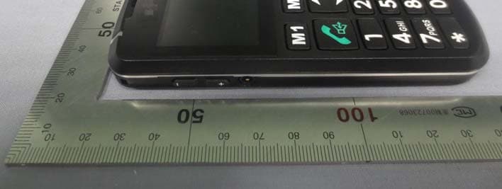
ACEPAL101V1
Jun 03, 2013Mobile phone
Equipment Class
DSS - Part 15 Spread Spectrum Transmitter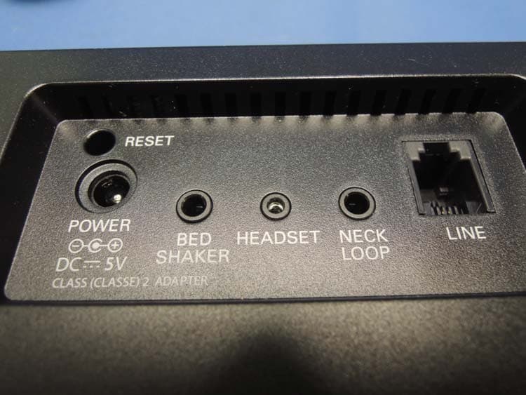
ACEENSEMBLE
Nov 29, 2012Corded Telephone with TAM and WiFi Feature
Equipment Class
DTS - Digital Transmission System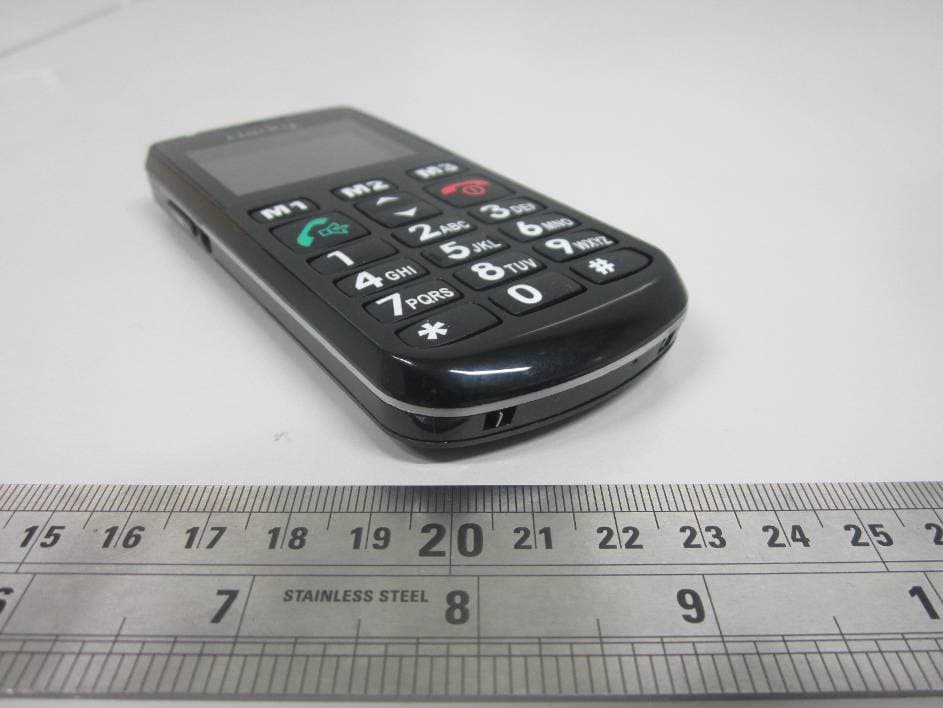
ACEPAL101
Jan 24, 2012GSM Senior Mobile Phone
Equipment Class
DSS - Part 15 Spread Spectrum Transmitter
ACEAL11RTXS
Jun 28, 2010Alert Master Home Alert System
Equipment Class
DSR - Part 15 Remote Control/Security Device Transceiver
ACED100TXS
Jun 28, 2010Doorbell
Equipment Class
DSC - Part 15 Security/Remote Control Transmitter