ADB9ZWFM3000VHF Radiotelephone
Furuno USA Inc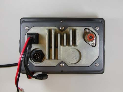
Click to zoom
Application Details
- Equipment Class
- GVH - Part 80 VHF Transmitter (GMDSS)
- Date of Grant
- May 11, 2005
- Application Purpose
- Original Equipment
- Date of Application
- Oct 01, 2003
- Equipment Note
- VHF Radiotelephone
- Frequency Range
- 156.02500000 - 157.42500000
- Company
- Furuno USA Inc
- Country
- United States
Documents & Files
Document Text
Text extracted from the exhibit documents filed with the FCC. Open a document above to read the original.
Users Manual
MARINE VHF RADIOTELEPHONE FM-3000 i Congratulations on your choice of the FURUNO FM-3000 Marine VHF Radiotelephone. We are confidentthat you will enjoy many years of trouble-free operationwith this fine piece of equipment.For more than 50 years FURUNO Electric Companyhas enjoyed an enviable reputation for quality and reli-ability throughout the world. This dedication is furtheredby our extensive global network of agents and dealers.Your equipment is designed and constructed to providecommercial grade performance and reliability, yet is af-fordable for pleasure craft owners.Please carefully read this manual and follow the rec-ommended procedure for installation, operation andmaintenance. With proper care, your equipment shouldprovide years of enjoyable and dependable communi-cations.Thank you for considering and purchasing FURUNO. D FEATURES ❍ Standard 4 ′′× 6 ′′ flush mount design ❍ Built-in DSC meets RTCM SC101 require-ment ❍ Rugged waterproof construction ❍ NMEA Input/Output ❍ Optional CONTROLLABLE MIC is con-nectable FOREWORDREAD ALL INSTRUCTIONS carefully and completely before using the transceiver. SAVE THIS INSTRUCTION MANUAL — This in- struction manual contains important operating instructions forthe FM-3000. IMPORTANT ii CLEAN THE TRANSCEIVER AND MICROPHONETHOROUGHLY WITH FRESH WATER after exposure to water including salt water, otherwise, the keys andswitches may become inoperable due to salt crystallization. IN CASE OF EMERGENCYIf your vessel requires assistance, contact other vessels andthe Coast Guard by sending a distress call on Ch 16.Or, transmit your distress call using digital selective calling onCh 70. USING CHANNEL 16DISTRESS CALL PROCEDURE1. “MAYDAY MAYDAY MAYDAY.”2. “THIS IS ...............” (name of vessel)3. Your call sign or other indication of the vessel (AND 9- digit DSC ID if you have one). 4. “LOCATED AT ...............” (your position)5. The nature of the distress and assistance required.6. Any other information which might facilitate the rescue.USING DIGITAL SELECTIVE CALLING (Ch 70) DISTRESS CALL PROCEDURE1. While lifting up the switch cover, push and hold [ [ DISTRESS DISTRESS ] ] for 5 sec. until you hear 5 short beeps change to one long beep. 2. Wait for an acknowledgment from a coast station. • Channel 16 is automatically selected. 3. Push and hold [ [ PTT PTT ] ] , then transmit the appropriate information as at above. NOTEA WARNING STICKER is supplied with the transceiver. To comply with FCC regulations, this sticker must be affixed insuch a location as to be readily seen from the operating con-trols of the radio as in the diagram below. Make sure the cho-sen location is clean and dry before applying the sticker. (p. viii)EXAMPLE iii Do not open the equipment.Only qualified personal should work inside the equipment.Do not disassemble or modify the equipment.Fire, electrical shock or serious injury can result.Turn off the power immediately if waterleaksinto the equipment or the equipment is em-mitting smoke or fire.Continued use of the equipment can cause fire or electricalshock.Any repair work must be done by a licensedradio technician.Improper repair work can cause electrical shock or fire. RR CAUTION BE CAREFUL! The transceiver and optional FM-3010 employ waterproof construction, which corresponds to JISwaterproof specification, Grade 7 (1 m/30 min.). However,once the transceiver or microphone has been dropped, wa-terproofing cannot be guaranteed due to the fact that thecase may be cracked, or the waterproof seal damaged, etc. AVOID the use of chemical agents such as benzine or al- cohol when cleaning, as they may damage the transceiversurfaces. RR CAUTION RR SAFTY INSTRUCTION For the operator Distances at which radiation levels of 100 and 10 W/m 2 exist are given in the table. Distance to Distance to 100 W/m 2 point 10 W/m 2 point 0.12 m 0.39 m iv ELECTRICAL SHOCK HAZARD Do not open the equipment un-less totally familiar with electri-cal circuits and service manual. Only qualified personal should work in-side the equipment. Be sure that the power supply is compatiblewith the voltage rating of the equipment.Connection of an incorrect power supply can cause fire orequipment damage. The voltage rating of the equipment ap-pears on the label above the power connector.Turn off the power at the switchboard beforebeginning the installation.Fire or electrical shock can result if the power is left on.DO NOT install the equipment where normal operation of the vessel may be hindered or where it could cause bodilyinjury. RR WARNING DO NOT cut the DC power cable between the DC plug and fuse holder. If an incorrect connection is made after cut-ting, the equipment may be damaged. RR WARNING Ground the equipment to pre- vent electrical shock and mutualinterference. Observe the following compass safe dis-tances to prevent interference to a magneticcompass: RR CAUTION For the installer Standard Steerling compass compass Transceiver 0.95 m 0.65 m Table of Contents v FOREWORD ............................................................. iIMPORTANT .............................................................. iIN CASE OF EMERGENCY ..................................... iiNOTE ........................................................................ iiSAFTY INSTRUCTION ............................................ iiiTable of Contents ..................................................... vSystem Configulation .............................................. viiStandard supply & Options .................................... viii1 Control ........................................................ 1 1.1 Front Panel ................................................... 11.2 Function Display ............................................ 31.3 Microphone .................................................... 4 2 Basic Operation ......................................... 5 2.1 Channel Selection ......................................... 52.2 Receiving and Transmitting ........................…
Text truncated - open the document above for the full version.
Operational Description
1 FM-3000 CIRCUIT DESCRIPTION 1 RECEIVER CIRCUITS 1-1 ANTENNA SWITCHING CIRCUIT (MAIN UNIT) The antenna switching circuit functions as a low-pass filter while receiving and as resonator circuit while transmitting. The circuit does not allow transmit signals to enter receiver circuits. Received signals enter the MAIN unit from the antenna con- nector and pass through the low-pass filter (L21, L22, C1, C127, C130). The signals are then applied to the RF circuit via the antenna switching circuit (D22, D23, R142, R144). 1-2 RF CIRCUIT (MAIN UNIT) The RF circuit amplifies signals within the range of frequen- cy coverage and filters out-of-band signals. The signals from the antenna switching circuit pass through a tunable bandpass filter (D25, L35, C149–C152) where the object signals are led to the RF amplifier circuit (Q21). The amplified signals at Q21 are applied to the other tunable bandpass filter (D26–D31, L36–L39, C161, C162, C164, C165, C173–C178, C182) to suppress unwanted signals and improve the selectivity. The signals are then applied to the 1st mixer circuit. D25–D31 employ varactor diodes, that are controlled by the PLL lock voltage, to track the band pass filters. 1-3 1ST MIXER AND 1ST IF CIRCUITS (MAIN UNIT) The 1st mixer circuit converts the received signal into a fixed frequency of the 1st IF signal with a 1st LO (VCO output) fre- quency. By changing the 1st LO frequency, only the desired frequency will pass through a pair of crystal filters at the next stage of the mixer. The signals from the RF circuit are mixed with the VCO sig- nals at the 1st mixer circuit (Q22) to produce a 21.7 MHz 1st IF signal. The 1st IF signal is applied to a pair of crystal filters (FI1, FI2) to suppress out-of-band signals and is then amplified at the IF amplifier (Q23). The amplified signal is applied to the 2nd mixer circuit (IC5). 1-4 2ND IF AND DEMODULATOR CIRCUITS (MAIN UNIT) The 2nd mixer circuit converts the 1st IF signal into a 2nd IF signal. A double superheterodyne system (which converts receive signals twice) improves the image rejection ratio and obtains stable receiver gain. The FM IF IC (IC5) contains the 2nd local oscillator, 2nd mixer, limiter amplifier, quadrature detector, and noise detector circuits, etc. The 1st IF signal from Q23 is applied to the 2nd mixer sec- tion of IC5 (pin 16), and is mixed with a 21.25 MHz 2nd LO signal generated at the PLL circuit using the reference fre- quency (21.25 MHz) to produce a 450 kHz 2nd IF signal. The 2nd IF signal from IC5 (pin 3) is passed through the ceramic filter (FI3), where unwanted signals are sup- pressed, and is then applied to the 2nd IF (limiter) amplifier in IC5 (pin 5). The signal is applied to the FM detector sec- tion in IC5 for demodulation into AF signals. The FM detector circuit employs a quadrature detection method (linear phase detection), which uses a ceramic dis- criminator (X2) for phase delay to obtain a non-adjusting cir- cuit. The detected signal from IC5 (pin 9) is applied to the AF circuit. 1-5 AF AMPLIFIER CIRCUIT (MAIN AND FRONT UNITS, VOL BOARD) The AF amplifier circuit amplifies the detected signals to drive a speaker. The AF circuit includes an AF mute circuit for the squelch. AF signals from IC5 (pin 9) are passed through the analog switch (IC16, pins 10, 11), and are applied to the de-empha- sis circuit (R291, C291). The de-emphasis circuit is an inte- grated circuit with frequency characteristic of –6 dB/octave. The integrated signals are applied to the active filters (Q35, Q36). Q35 functions as a high-pass filter to suppress unwanted lower noise signals and Q36 functions as a low- pass filter to suppress higher noise signals. The filtered signals are passed through the [VOLUME] con- trol on the VOL board, and are then applied to the AF power amplifier (IC14, pin 1). The output signal from IC14 (pin 4) drives the internal (external) speaker (FRONT unit). 1-6 SQUELCH CIRCUIT (MAIN UNIT) A squelch circuit cuts out AF signals when no RF signals are received. By detecting noise components in the AF signals, the squelch circuit switches the AF mute switch. A portion of the AF signals from the FM IF IC (IC5, pin 9) pass through the squelch adjustment pot (R214), and are then applied to the active filter section (IC5, pin 8). The active filter section amplifies and filters noise components. The filtered signals are applied to the noise detector section and output from pin 14. The signal is amplified at the SQL amplifier (IC6) and applied to the CPU (IC19, pin 39) as the “SQL” signal. The CPU analyzes the noise condition and outputs the “RMUTM”, “RMUTS” signals to toggle the AF mute switches (Q37, Q38). 2 2 TRANSMITTER CIRCUITS 2-1 MICROPHONE AMPLIFIER CIRCUIT (MAIN UNIT) The microphone amplifier circuit amplifies audio signals with +6 dB/octave pre-emphasis from the microphone to a level needed at the modulation circuit. The AF signals from the microphone are amplified at the microphone amplifier (IC15a, pin 2) via the analog switch (IC13, pins 11, 10). A capacitor (C367) and resistor (R369) are connected to the amplifier to obtain the pre-emphasis characteristics. The amplified signals are applied to the IDC amplifier (IC17a, pin 2) via the analog switch (IC16, pins 9, 8 and pins 4, 3) and are passed through the splatter filter (IC17b) to suppress unwanted 3 kHz or higher signals. The filtered sig- nals are then applied to the modulation circuit. 2-2 MODULATION CIRCUIT (MAIN UNIT) The modulation circuit modulates the VCO oscillating signal (RF signal) using the microphone audio signals. Audio signals from the splatter filter (IC17b) pass through the frequency deviation adjustment pot (R381) and are then applied to the modulation circuit (D1–D3) to change the reactance of D3, and modulate the oscillated signal at the TX-VCO (Q4). 2-3 DRIVE AMPLIFIER CIRCUIT (MAIN UNIT) The drive amplifier circuit amplifies the VCO oscillating sig- nal to a level needed at the power amplifier. The VCO output is buffer-amplifie…
Text truncated - open the document above for the full version.
Test Report
1 FM-3000 CIRCUIT DESCRIPTION 1 RECEIVER CIRCUITS 1-1 ANTENNA SWITCHING CIRCUIT (MAIN UNIT) The antenna switching circuit functions as a low-pass filter while receiving and as resonator circuit while transmitting. The circuit does not allow transmit signals to enter receiver circuits. Received signals enter the MAIN unit from the antenna con- nector and pass through the low-pass filter (L21, L22, C1, C127, C130). The signals are then applied to the RF circuit via the antenna switching circuit (D22, D23, R142, R144). 1-2 RF CIRCUIT (MAIN UNIT) The RF circuit amplifies signals within the range of frequen- cy coverage and filters out-of-band signals. The signals from the antenna switching circuit pass through a tunable bandpass filter (D25, L35, C149–C152) where the object signals are led to the RF amplifier circuit (Q21). The amplified signals at Q21 are applied to the other tunable bandpass filter (D26–D31, L36–L39, C161, C162, C164, C165, C173–C178, C182) to suppress unwanted signals and improve the selectivity. The signals are then applied to the 1st mixer circuit. D25–D31 employ varactor diodes, that are controlled by the PLL lock voltage, to track the band pass filters. 1-3 1ST MIXER AND 1ST IF CIRCUITS (MAIN UNIT) The 1st mixer circuit converts the received signal into a fixed frequency of the 1st IF signal with a 1st LO (VCO output) fre- quency. By changing the 1st LO frequency, only the desired frequency will pass through a pair of crystal filters at the next stage of the mixer. The signals from the RF circuit are mixed with the VCO sig- nals at the 1st mixer circuit (Q22) to produce a 21.7 MHz 1st IF signal. The 1st IF signal is applied to a pair of crystal filters (FI1, FI2) to suppress out-of-band signals and is then amplified at the IF amplifier (Q23). The amplified signal is applied to the 2nd mixer circuit (IC5). 1-4 2ND IF AND DEMODULATOR CIRCUITS (MAIN UNIT) The 2nd mixer circuit converts the 1st IF signal into a 2nd IF signal. A double superheterodyne system (which converts receive signals twice) improves the image rejection ratio and obtains stable receiver gain. The FM IF IC (IC5) contains the 2nd local oscillator, 2nd mixer, limiter amplifier, quadrature detector, and noise detector circuits, etc. The 1st IF signal from Q23 is applied to the 2nd mixer sec- tion of IC5 (pin 16), and is mixed with a 21.25 MHz 2nd LO signal generated at the PLL circuit using the reference fre- quency (21.25 MHz) to produce a 450 kHz 2nd IF signal. The 2nd IF signal from IC5 (pin 3) is passed through the ceramic filter (FI3), where unwanted signals are sup- pressed, and is then applied to the 2nd IF (limiter) amplifier in IC5 (pin 5). The signal is applied to the FM detector sec- tion in IC5 for demodulation into AF signals. The FM detector circuit employs a quadrature detection method (linear phase detection), which uses a ceramic dis- criminator (X2) for phase delay to obtain a non-adjusting cir- cuit. The detected signal from IC5 (pin 9) is applied to the AF circuit. 1-5 AF AMPLIFIER CIRCUIT (MAIN AND FRONT UNITS, VOL BOARD) The AF amplifier circuit amplifies the detected signals to drive a speaker. The AF circuit includes an AF mute circuit for the squelch. AF signals from IC5 (pin 9) are passed through the analog switch (IC16, pins 10, 11), and are applied to the de-empha- sis circuit (R291, C291). The de-emphasis circuit is an inte- grated circuit with frequency characteristic of –6 dB/octave. The integrated signals are applied to the active filters (Q35, Q36). Q35 functions as a high-pass filter to suppress unwanted lower noise signals and Q36 functions as a low- pass filter to suppress higher noise signals. The filtered signals are passed through the [VOLUME] con- trol on the VOL board, and are then applied to the AF power amplifier (IC14, pin 1). The output signal from IC14 (pin 4) drives the internal (external) speaker (FRONT unit). 1-6 SQUELCH CIRCUIT (MAIN UNIT) A squelch circuit cuts out AF signals when no RF signals are received. By detecting noise components in the AF signals, the squelch circuit switches the AF mute switch. A portion of the AF signals from the FM IF IC (IC5, pin 9) pass through the squelch adjustment pot (R214), and are then applied to the active filter section (IC5, pin 8). The active filter section amplifies and filters noise components. The filtered signals are applied to the noise detector section and output from pin 14. The signal is amplified at the SQL amplifier (IC6) and applied to the CPU (IC19, pin 39) as the “SQL” signal. The CPU analyzes the noise condition and outputs the “RMUTM”, “RMUTS” signals to toggle the AF mute switches (Q37, Q38). 2 2 TRANSMITTER CIRCUITS 2-1 MICROPHONE AMPLIFIER CIRCUIT (MAIN UNIT) The microphone amplifier circuit amplifies audio signals with +6 dB/octave pre-emphasis from the microphone to a level needed at the modulation circuit. The AF signals from the microphone are amplified at the microphone amplifier (IC15a, pin 2) via the analog switch (IC13, pins 11, 10). A capacitor (C367) and resistor (R369) are connected to the amplifier to obtain the pre-emphasis characteristics. The amplified signals are applied to the IDC amplifier (IC17a, pin 2) via the analog switch (IC16, pins 9, 8 and pins 4, 3) and are passed through the splatter filter (IC17b) to suppress unwanted 3 kHz or higher signals. The filtered sig- nals are then applied to the modulation circuit. 2-2 MODULATION CIRCUIT (MAIN UNIT) The modulation circuit modulates the VCO oscillating signal (RF signal) using the microphone audio signals. Audio signals from the splatter filter (IC17b) pass through the frequency deviation adjustment pot (R381) and are then applied to the modulation circuit (D1–D3) to change the reactance of D3, and modulate the oscillated signal at the TX-VCO (Q4). 2-3 DRIVE AMPLIFIER CIRCUIT (MAIN UNIT) The drive amplifier circuit amplifies the VCO oscillating sig- nal to a level needed at the power amplifier. The VCO output is buffer-amplifie…
Text truncated - open the document above for the full version.
Contact Information
Applicant
Bill Haynes(Deep Sea Product Manager)
Technical Specifications
| # | Rule Parts | Frequency Range | Power Output | Emission | Tolerance |
|---|---|---|---|---|---|
| 4 | 80.1101(c)(4) | 156.025 MHz - 157.425 MHz | 1 W | 16K0G2B | 10 ppm |
Other Applications from Furuno USA Inc
ADB-9ZWRTR137
Feb 18, 2026Transceiver unit for the radar sensor
Equipment Class
MRD - Marine RadarADB9ZWRTR136
Jul 01, 2024Transceiver unit for the radar sensor
Equipment Class
MRD - Marine Radar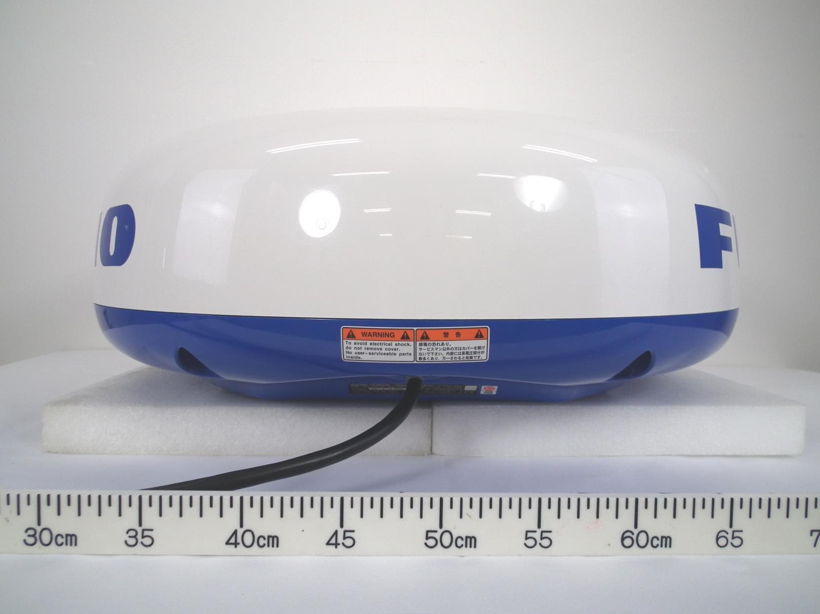
ADB9ZWRTR128
Apr 06, 2022Transceiver unit for the radar sensor
Equipment Class
MRD - Marine Radar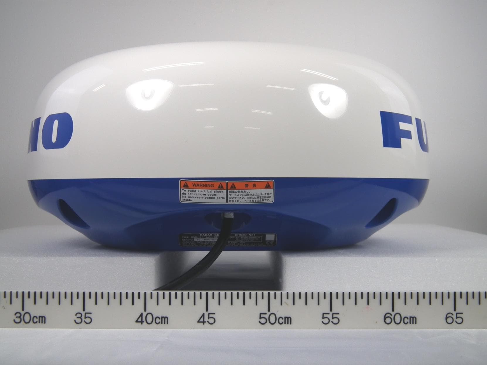
ADB9ZWRTR133
Sep 26, 2021Transceiver unit for the radar sensor
Equipment Class
MRD - Marine Radar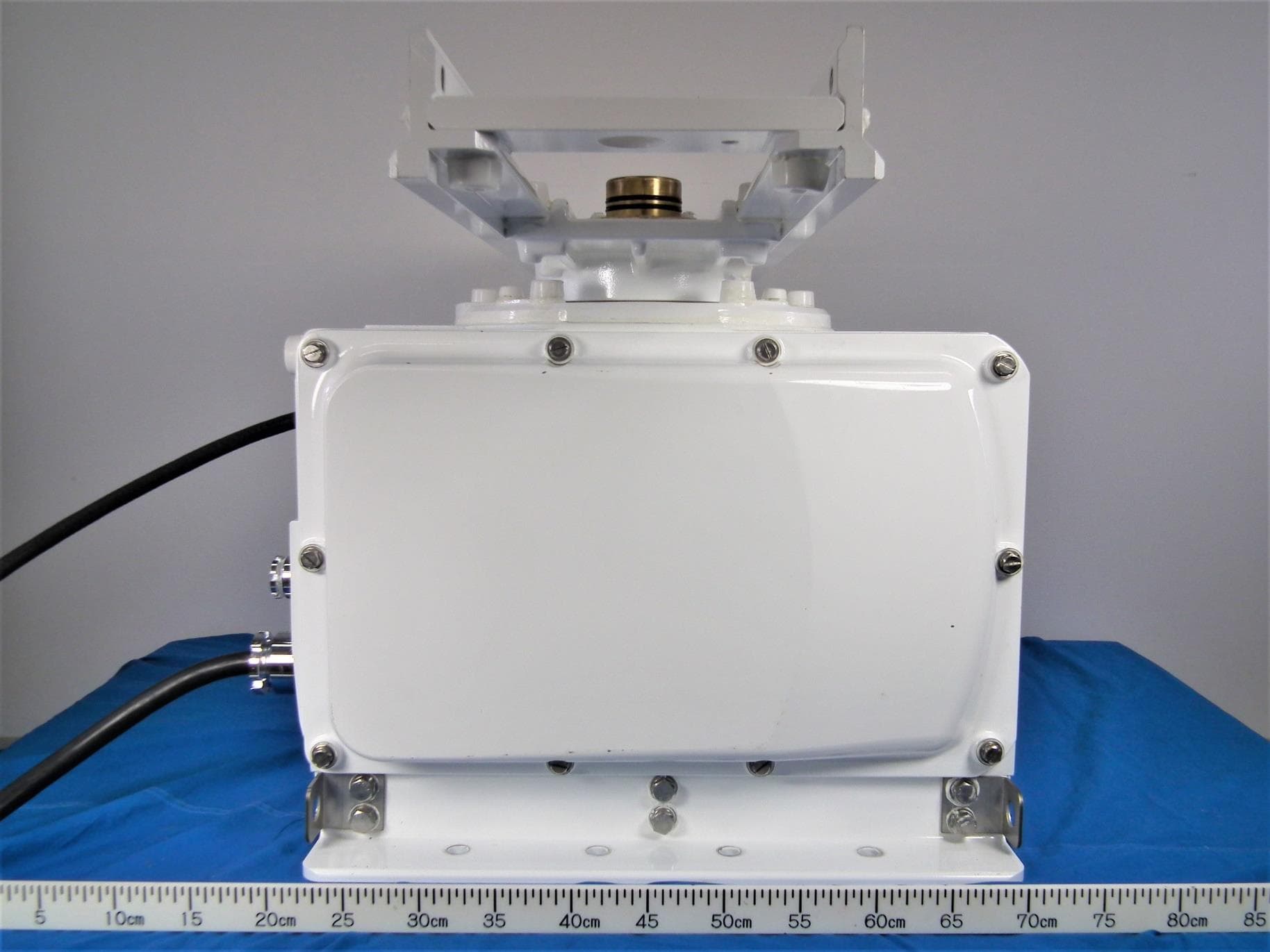
ADB9ZWRTR129
May 23, 2021Transceiver unit for the radar sensor
Equipment Class
MRD - Marine Radar