AFJIC-2800HReceiver Portion of Amateur Transceiver
ICOM Incorporated
Click to zoom
Application Details
- Equipment Class
- CSR - Scanning Receiver
- Date of Grant
- Apr 04, 1999
- Application Purpose
- Original Equipment
- Date of Application
- Feb 10, 1999
- Equipment Note
- Receiver Portion of Amateur Transceiver
- Frequency Range
- 430.00000000 - 450.00000000
- Company
- ICOM Incorporated
- Country
- Japan
Documents & Files
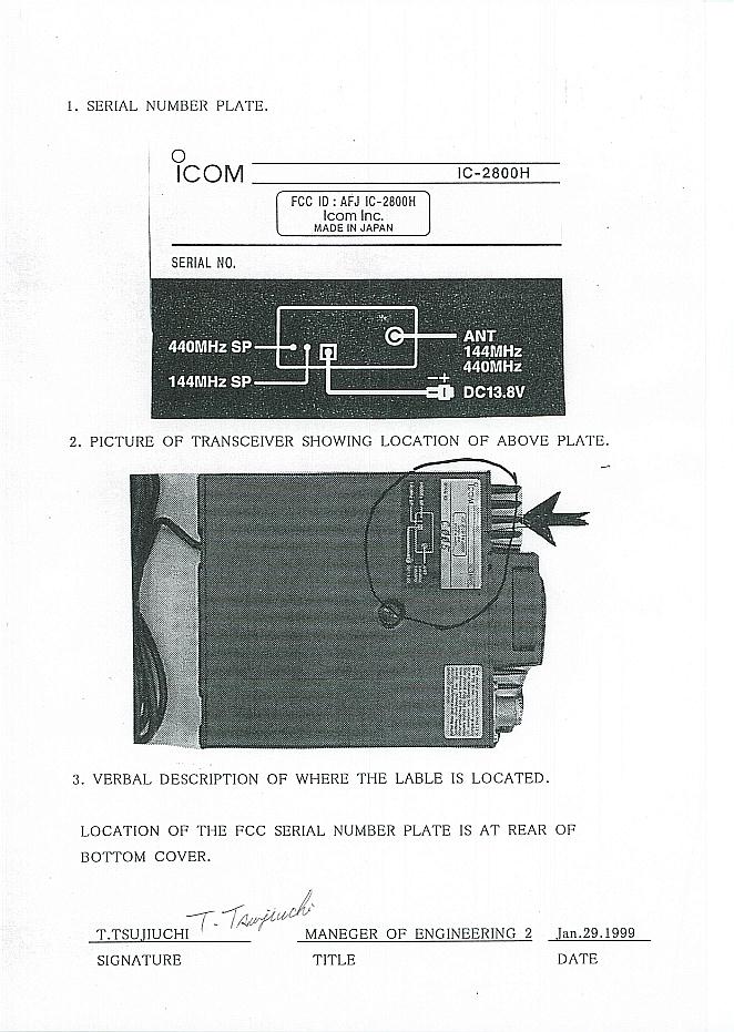
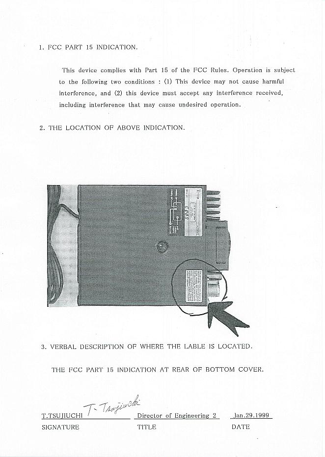
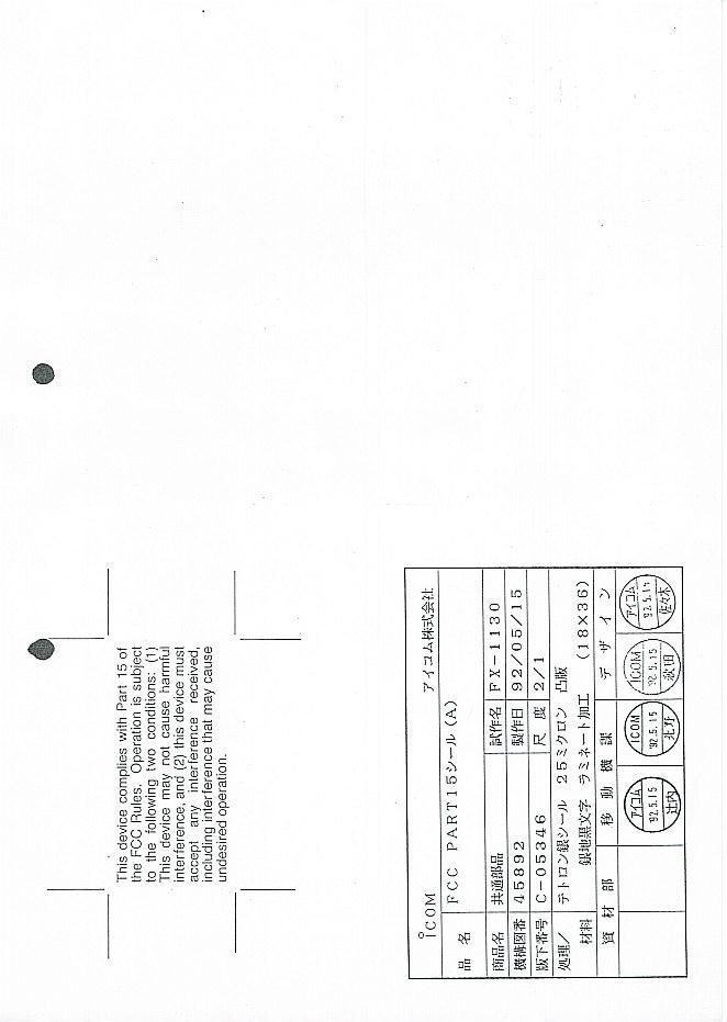
Document Text
Text extracted from the exhibit documents filed with the FCC. Open a document above to read the original.
Users Manual
INSTRUCTION MANUAL This device complies with Part 15 of the FCC rules. Operation is sub-ject to the following two conditions: (1) This device may not causeharmful interference, and (2) this device must accept any interferencereceived, including interference that may cause undesired operation. i2800HDUAL BAND FM TRANSCEIVER i FOREWORDREAD ALL INSTRUCTIONS carefully and completely before using the transceiver. SAVE THIS INSTRUCTION MANUAL — This in- struction manual contains important operating instructions forthe IC-2800H. EXPLICIT DEFINITIONSThe explicit definitions below apply to this instruction manual. CAUTIONSR WARNING! NEVER connect the transceiver to an AC outlet. This may pose a fire hazard or result in an electricshock.R WARNING! NEVER operate the transceiver while dri- ving a vehicle. Safe driving requires your full attention—any-thing less may result in an accident. R WARNING! HIGH VOLTAGE! NEVER disassem- ble the remote controller. There is a high voltage circuit inside. NEVER connect the transceiver to a power source of more than 16 V DC or using reverse polarity. This will ruin the trans-ceiver. NEVER cut the DC power cable between the DC plug and fuse holder. If an incorrect connection is made after cutting,the transceiver may be damaged. NEVER place the transceiver where normal operation of the vehicle may be hindered or where it could cause bodily injury.NEVER let objects impede the operation of the cooling fan on the rear panel. DO NOT push the PTT when not actually desiring to trans- mit. WORD R WARNING CAUTION NOTE DEFINITION Personal injury, fire hazard or electric shock may occur.If disregarded, inconvenience only. No risk of personal injury, fire or electric shock.Equipment damage may occur. Versions of the IC-2800H which display the “CE” symbol on the se-rial number seal comply with the European harmonised standardETS300 684 (EMC product standard for Commercially AvailableAmateur Radio Equipment). ii DO NOT operate the transceiver near unshielded electrical blasting caps or in an explosive atmosphere.During mobile operation, DO NOT operate the transceiver without running the vehicle’s engine. When transceiver poweris ON and your vehicle’s engine is OFF, the vehicle’s batterywill soon become exhausted. AVOID using or placing the transceiver in direct sunlight or in areas with temperatures below –10°C (+14°F) or above+60°C (+140°F). AVOID the use of chemical agents such as benzine or alco- hol when cleaning, as they can damage the transceiver’s sur-faces.Place unit in a secure place to avoid inadvertent use by chil-dren. BE CAREFUL! The transceiver will become hot when op- erating it continuously for long periods. USE Icom microphones only (supplied or optional). Other manufacturer’s microphones have different pin assignmentsand may damage the transceiver if attached. For LCD displayDO NOT press the LCD screen. Excessive pressure may cause permanent damage to the LCD. DO NOT tap or scratch the LCD using sharp objects. BE CAREFUL when cleaning the LCD. Dust can easily scratch the surface.LCDs are produced using high-density manufacturing tech-nology resulting in 99.98% active dots, however, up to 0.02%of the dots may be non-active and/or continuously active. Thisis normal and does not indicate LCD malfunction.Uneven areas may be displayed depending on display con-tents in some cases.After displaying the same screen continuously for long peri-ods, image ‘burn-in’ may occur. In such cases, turn the powerOFF and discontinue operation for at least 24 hours. For U.S.A. onlyCAUTION: Changes or modifications to this device, not ex- pressly approved by Icom Inc., could void your authority tooperate this device under FCC regulations. 1 SUPPLIED ACCESSORIES ......... 12 PANEL DESCRIPTION ......... 2 – 13 n Controller unit ......................... 2 n Function display ...................... 4 n Basic function menu ............... 6 n Main unit ................................. 8 n HM-98 microphone ............... 10 n HM-97/118 microphone ........ 13 3 INSTALLATION ................... 14 – 17 n Location ................................ 14 n Mounting with the mountingbracket .................................. 14 n Mounting the remote controller ............................... 15 n Battery connection ................ 15 n DC power supply connection ............................ 16 n Cable connection .................. 16 n Antenna installation .............. 17 4 FREQUENCY SETTING ...... 18 – 22 n Preparation ........................... 18 n Lock functions ....................... 19 n Using the tuning dial ............. 20 n Using the [ Y ]/[ Z ] keys .......... 20 n Setting a tuning step ............. 21 n Using the keypad .................. 22 5 BASIC OPERATION ............ 23 – 25 n Receiving .............................. 23 n Monitor function .................... 24 n Audio mute function .............. 24 n Transmitting .......................... 24 n Selecting output power ......... 25 n One-touch PTT function ....... 25 6 REPEATER OPERATION .... 26 – 31 n Accessing a repeater ............ 26 n 1750 Hz tone ........................ 28 n Subaudible tone .................... 29 n Offset frequency ................... 30 n Auto repeater function .......... 31 7 MEMORY/CALL CHANNELS ......................... 32 – 39 n General ................................. 32 n Programming during selection................................. 32 n Programming after selection .. 33 n Transferring memory contents to another memory ............... 33 n Programming during selectionvia the microphone ............... 34 n Programming after selection via the microphone ............... 34 n Transferring memory contents to another memory via themicrophone ........................... 35 n Memory clear ........................ 36 n Alphanumeric display ............ 37 n Call channel .......................... 38 8 SCRATCH PAD MEMORY ... 40 – 41 n What is a scratch pad memory? ............................... …
Text truncated - open the document above for the full version.
Block Diagram
DATE1998.12.09MODEL DWN.NO. APPD.CHKD. DWN.BY: 1 2 3 4 5 6 REVISIONS ICOMIcom Inc FX-2047 ABCDE ABCDE 6 5 4 3 2 1 6 5 4 3 2 1 7 8 9.. . .. . .. .. .. .. .. .. DIAGRAM CONTROL BLOCK 5B1 CPU X2 CTRL5V REG VDLA VDLB VVOLV VSQLV VDIAL VVOL VSQL UDLA UDLB UDIAL UVOL USQL USQLV UVOLV F-1 F-5 CHGK PWRK K1V K2V 12.288MHz IC14 CTRL HVSW Q16 Q17 IC15 -15V REG Q14,Q15 D-RAM IC9 COLOR GRAPHICS IC8 IC6 TFT LCD INTERFACE DC-DC X3 IC19 CLKI G B IN/EXT IC16 X1 3.579545MHz CS,WR,RD,FAI Q11 IC2 R G B CR-566 CFL DRIVE -DD9 S-80945ANMP RESET IC11 TFT CONTROLLER IC1 MN83951 IC7 TC7W14FU M/ESW PWRS BRITV CONTV SP MA0 ~ MA 8 MD0~ MD15 TDATA HV RDATA GND SP SPE WR,RD, FAI LRES WAIT A0~A18 D0~D7 XTAL EXTAL IC10 Q12 2SC4081 2SC4081 TC7W04FU M52042FP M52045FP #02,03,12,13 NTSC/PAL VIDEO CHROMA INVERTER LCD CONTROLLER SED1354F0A TC75S51F D2 1SV282 TA78L05F DTC144EU CONVERTER TA79L15F CPH1,CPH2,CPH3, STH1,OEH,Q2H, STV2,OEV, CPV,STV1 DS1 R TXD RXD EXTV Q5,Q8 2SC4081x2 Q6,Q7 2SA1576X2 2SA1576X2 Q2,Q3 2SC4081x2 Q1,Q4 M52338FP VIDEO AMP PD AMP IC21 OCTAL BUS IC20 TC7S08FU BUFFER CHG/L VCOM DIAMOND AMP DIAMOND AMP VGL RES TFT COLOR LCD F-2 F-3 F-4 F-6 F-7 F-8 POWER HD6433032SK 2SA1362 IC3 M5291FP Q21 2SB798 SB10-05PCPD3 Q18 2SB1132 D1 1SS355 COM OUT Q13 2SA1576 to MAIN UNIT TDATA RDATA BUFFER AMP BUFFER AMP EDTCA22QB0 TC74AC244F -60A LH61665AS CSTC26.25MXJ040 +5V REG IC17,IC22, TA78L05Fx3 IC23 Q19 DTC144EU Q20 2SA1362 2SC3647x2 D9 1SS355 A/B/C R G B CR-640 CTRL5V -15V -15V -15V J2 1 2 3 4 5 6 J4 13.8V-15V 13.8V +3V REG D10 MA8030 CFL +5VA +5VB +5VC -3V REG D11 MA8030 +5VC +5VC +5VB +5VC +4V REG D14 MA8047 +3V REG D12 MA8033 +5VC -15V +5VA +4V REG D13 MA8043 CTRL5V 9 8 7 6 5 4 3 2 ABCD EGIJKLMN 11 1 0 ABCDEFGHIJKLMN 1 0 9 8 7 6 5 4 3 2 FX-2047..199808 ICOMIcom Inc REVISIONS DIAGRAM 1 2 3 4 5 6.. .. .. .. .. .. H 7 8 9 10 11 12.. .. .. .. .. ..MODEL DWN.NO. DATEAPPD.CHKD. DWN.BY: CRYSTAL FIL FI1 FL-288 430~450MHzRX/TX 1SS355 118~174MHz 144~148MHz RX TX D16 1SS355D7,D8 V_LOOP FIL 2SC5085x2 V_MOD MUTE V_VCO8 REG D25,D26 U_LOOP FIL 2SC4081 U_VCO8 REG FI3 Q15 3SK166 2SC4081 UT8V REG VT8V REG DTB123EK FAN CTRL 2SC4081 MA8075 TA7808F 8V REG MDATA CONT TA75S01F X4 SMD-49 Q35 Q34 DTB123EK HI/LOW CTRL IC5 TA75S01F TA7805F MATRIX INITIAL 2SC4081 1SS355 MA8062 OSC1 OSC2 E2PROM IC17ESO POWER SW CTRL D/A CTRL M62354GP 2SC4081 2SC4081 2SC4081x2 2SC4081x2 2SC4213 AF AMP LA4445 IC12 U_AF FIL V_AF FIL 2SC4213 2SC4213 COM_MUTE IC11 TC4S81F U_MUTEU_MON AMP V_MON AMP *OPTION UNIT DTMF DEC (UT-49) PROTECTER DTC144EU MA77 X1 CR-549 M64076AGP UUNLK MICIN VAMUTE UAMUTE UATT VATT 5B2 BLOCK MAIN UNIT CPU HD6433876N Q18 2SK880 IC2 IC19 MA8091 PLL5V DTC144EU DTB123EK HVU350 D4 MA862 V_PAV_APC DETV_ANT SWV_LO SW 1SV284x2 U_LO SWU_APC DET TX 144~148MHz RX 120.35~158.35MHz RX 383.95~403.95MHz TX 430~450MHz MU/D PROTECTER D67 MA728 9600bps AMP IC27B IC27A FIL D40 MA8047 CDB450C24 X2 LPF IDC AMP MIC AMP NJM4558M NJM4558M 2SC4081 MIC MIC MUTE MDATA MICE EXTMIC MIC SENS. CTRL 15.65MHz M67746 V_RF AMP Q16 3SK166 D11,D12,D13 D14 1SS355 HVU350x3V_MIX BUFF AMP Q7 2SC5085 BUFF AMP Q6 2SC5085 BUFF AMP Q8 2SC5193 PLL 15.2MHz V_SHIFT Q3 D2 Q2 2SC4213 Q40 2SC4215 D30 MA133 NOISE LVO1 LVO2 LVO3 LVO4 IC4 SC-1318 U_MIX FIL CERAMIC FIL FI6D42 MA8047 CDB450C24 X3 IC8 TA31136FN NOISE FIL FI2 FL-300 46.05MHz F U_VCO FRQ. SDET,NOISEAMP,SQLSW,AFFIL U_MIX,OSC,IFAMP,FMDET, V_MIX,OSC,IFAMP,FMDET, SDET,NOISEAMP,SQLSW,AFFIL V_IF5V REG U_IF5V REG U_CRYSTAL U_BPFU_RF AMP Q44 3SK166 DATAIN PTTP AFOUT DATAOUT M62429FP IC10 VOL CTRL D44 Q76 Q77 MIC8V SW Q90 2SD999 Q91 DTA144EU Q92 DTC114EU D64 MA8091 D65 1SS355 U BIAS SEL V BIAS SEL RX RX/TX TX DATABUS Q81 Q87 Q85,Q86 Q83,Q84 Q69 Q70 Q71 U_VCO Q20,Q21 2SC4228x2 D20,D21 D22 MA862 D23 MA77 D35 1SS355 UMG9N 1/2 383.95~393.95MHz 120.35~158.35MHz D9 UM9401F RB706Fx2 IC1 V_VCO Q4,Q5 D3 V_IF AMP IC3 IC28 TA31136FN IC14 D45 DSA3A1 D46 RD20E 2SB1132 Q36 UMG9N 1/2 Q34 DTB123EK Q37 Q38 UMG9N 1/2 DTB123EK Q37 Q39 UMG9N 1/2 300M BIAS SEL BIAS SEL 800M D61 Q78 D47 IC24 D63 RES C5V REG IC15 X25320SI ESI,ECS, ESCK VSOUT USOUT 1RX4RX3RX8RX PCTRL FANC IS0,IS1,IS2 II0,II1, II2,II3 U8V SW IC23A 1/2 IC23B 1/2 Q88 IC26 BU4066BCFV Q93 DTC144EU IC25 TC7S66FU NJM4558M 1/2 D68 RB706F 9600bps LIMIT NJM4558M 1/2 9600bps SW MMUTE,DTMUTE,MRIPTDTMF,ETONE DTC143XU 2SB1201 Q75 Q74 CTCSS MIC SEL D62 1SS355 PTTM PSQL PSQL SW Q73 DTC144EU Q13 Q14 Q1 D1 Q17 D19 1SS355 V_DC-AMP TONE FIL IC20 NJM4558M CLONE BUFF Q98 DTC144TU DATA,CK,PLSTB,STB HV TDATA RDATA GND SP SPE MU/D EXTMIC PSEL PSQL LIMIT VTX UTX USQL PTTP RXDF VUNLK 800_MIX DUBLER AMP Q68 2SC5085 Q41 2SC5193 D31 MA133 U_IF AMP 800_ATT CTRL Q46 2SC4081 Q45 2SC4081 U_ATT CTRL 300_RF AMP Q47,Q48 2SC4226x2 U_RF SW U_RF SW D36 MA862 U_AM DET U_AGC V_AM DET V_AGC UMMUTE VAM LV UAM VMMUTE VSHIFT TONEIN 3LB VSQL V_MUTE PTTP CTRL Q96 2SC4081 D73 1SS355 IC13 Q72 SELECTOR DET SELECTOR IC21 BU4066BCFV Q82 DTC144EU IC29 RESET IC16 S-80945ALMP-DA9 U_MOD MUTE Q19 2SC4213 Q9 2SC4081 2SA1362 Q10 Q25 2SC4081 Q26 2SA1362 D28 1SS355 D29 DAN202U D66 1SS355 V_DRIVE Q12 2SC2954 D5 DA221 D6 1SS355 Q11 2SC3357 V_PRI DRIVE Q57,Q59 2SK880x2 D41 RB706F V_ATT CTRL Q33 2SC4081 APC CTRL EFCH445MWNP1 EFCH435 MWNP1 D32 DAN202U Q43 3SK184 Q42 DTC144EU BU4066BCFV DTC144EU Q50 3SK184 Q49 DTC144EU Q51 2SC5085 D70 MA8043 UPC1676G IC9 800_RF AMP U_PA HVU131TRF D72 D37 1SS355 D27 UM9401F U_ANT SW U_DRIVE Q29 2SC2954 D24 DA221 U_PRI DRIVE Q28 2SC3357 U_LO BUFF Q27 2SC5085 BUFF AMP Q24 2SC5085 BUFF AMP Q22 2SC5085 BUFF AMP Q23 2SC5193 Q64,Q65 2SK880x2 D43 RB706F Q62 2SJ144 Q63 2SC4081 Q55 2SJ144 Q56 2SC4081 CERAMIC FIL FI4 ALFY450F=K BPF BPF D15 HVU350 D71 1SS355 POW CTRL D/A E MU/D M8V VDATA,VCK Q3,Q4,OPD STD,Q1,Q2, VDMUTE,UDMUTE,DMAIN CLONEC,TMAIN,TXDF TONE,DATA BU4053BCFV SELECTOR PACKET DET D18 UM9401F D39 UM9401F RB706Fx2 U-1st Lo V-1st Lo Q61 DTC144EU Q53 DTC144EU V_DET SW U_DET SW PTT PTTM CTRL Q79 2SA1576 Q80 2SC4081 12 CONTROL UNIT FROM + - U-2nd Lo:45.6MHz V-2nd Lo:15.2MHz VSQL VSOUT USQL USOUT input POWER DC 13.8V PO CTRL(8Bit) PO CTRL(8Bit) DAT…
Text truncated - open the document above for the full version.
Operational Description
4 - 1 SECTION 4 CIRCUIT DESCRIPTION 4-1 RECEIVER CIRCUITS 4-1-1 DUPLEXER CIRCUIT The transceiver has a duplexer (low-pass and high-pass fil- ters) on the first stage from the antenna connector to sepa- rate the signals into VHF and UHF signals. The low-pass fil- ter (L15, L16, L78, C70–C72) is for VHF signals and the high- pass filter (L44, L45, L82, C189, C190, C493) is for UHF sig- nals. The separated signals are applied to each RF circuit. 4-1-2 VHF ANTENNA SWITCHING CIRCUIT The antenna switching circuit functions as a low-pass filter while receiving. However, its impedance becomes very high while transmitting by turning ON diode (D18). Thus transmit signals are blocked from entering the receiver circuits. The antenna switching circuit employs a 1/4 λtype diode switch- ing system. The passed signals are then applied to the VHF RF amplifier circuit. 4-1-3 VHF SQUELCH ATTENUATOR CIRCUIT The attenuator circuit attenuates the signal strength to a maximum of 10 dB to protect the RF amplifier from distortion when excessively strong signals are received. The current flow of the antenna switching circuit (D18) is con- trolled by the [SQL] control via Q33. When the [SQL] control is rotated clockwise deeper than 12 o’clock, the current of D18 is increased. In this case, D18 acts as an attenuator. 4-1-4 VHF RF CIRCUIT The RF circuit amplifies signals within the range of frequen- cy coverage and filters out-of-band signals. The signals from the antenna switching circuit pass through the tunable bandpass filter (D15, L25, L26, C115–C117). The filtered signals are amplified at the VHF RF amplifier (Q16) and are then enter another 3-stage tunable bandpass filter (D11–D14, L20–L21, C94, C96–C105) to suppress unwant- ed signals. and improve the selectivity. The filtered signals are applied to the VHF 1st mixer circuit (Q15).The tunable bandpass filters (D11–D13, D15) employ varactor diodes to tune the center frequency of the RF passband for wide band- width receiving and good image response rejection. The PLL lock voltage is used for control voltage of these varactor diodes. The PLL lock voltage is amplified at the DC-amplifier (Q18) and then applied to the CPU (IC19, pin 99). The CPU outputs the control signal to the varactor diodes via the D/A converter (IC3). 4-1-5 VHF 1ST MIXER CIRCUIT The 1st mixer circuit converts the received signal to a fixed frequency of the 1st IF signal with a 1st LO (V-VCO output) frequency. The signals from the VHF RF circuit are mixed with the 1st LO signal at the 1st mixer circuit (Q15) to produce a 15.65 MHz 1st IF signal. 4-1-6 VHF 1ST IF CIRCUIT By changing the PLL frequency, only the desired frequency will pass through a pair of crystal filters at the next stage of the mixer. The 1st IF signal from the VHF 1st mixer circuit is applied to a pair of crystal filters (FI1) to suppress out-of-band signals via a matching circuit (R61, C88). The filtered signal is ampli- fied at the IF amplifier (Q40) and is then applied to the VHF 2nd mixer circuit (IC28). 4-1-7 VHF 2ND IF AND DEMODULATOR CIRCUITS The 2nd mixer circuit converts the 1st IF signal to a 2nd IF signal. A double superheterodyne system (which converts receive signals twice) improves the image rejection ratio and obtains stable receiver gain. The FM IF IC (IC28) contains the 2nd local oscillator, 2nd mixer, limiter amplifier, quadrature detector, and noise detec- tor circuits, etc. The 1st IF signal from the 2nd IF amplifier is applied to the 2nd mixer section of IC28 (pin 16), and is mixed with a 15.2 MHz 2nd LO signal generated by the reference oscillator cir- cuit (X1, IC2) to produce a 450 kHz VHF 2nd IF signal. The 2nd IF signal from the 2nd mixer passes through the 2nd IF filter (FI4) (during wide channel spacing selection, or pass- es through FI5 during narrow channel spacing selection; [EUR], [ITA] versions only), where unwanted signals are suppressed. It is then amplified at the limiter amplifier section (IC28, pin 5) and applied to the FM detector section (X2, IC28, pins 10, 11) for demodulation the 2nd IF signal into AF signals. The FM detector circuit employs a quadrature detection method (liner phase detection), which uses a ceramic dis- criminator (X2) for phase delay to obtain a non-adjusting cir- cuit. The detected signal from IC28 (pin 9) is applied to the AF circuit. 4-1-8 VHF AF AMPLIFIER CIRCUIT The AF amplifier circuit amplifies the detected signals to drive a speaker. The AF circuit includes an AF mute circuit for the squelch. AF signals from FM IF IC (IC28, pin 9) pass through the AF selector (IC21, pins 9, 8), and are then applied to the low- pass (Q83, R370–R373, C406–C409) and high-pass (Q84, R375–R379, C415–C418) filters. The filtered signals are level adjusted at the volume control IC (IC10), and are ampli- fied at the AF power amplifier (IC12, pin 2) passing through the V-AF mute switch (Q70). The output signal from IC12 (pin 11) drives the external or internal speaker. 4 - 2 4-1-9 VHF SQUELCH CIRCUIT • NOISE SQUELCH A noise squelch circuit cuts out AF signals when no RF sig- nals are received. By detecting noise components in the AF signals, the squelch circuit switches the AF mute switch. Some of the noise components in the AF signals from the FM IF IC (IC28, pin 9) are passed through the active filter section (IC28, pin 8, 7), and then applied to the noise detector sec- tion (IC28). The variable resister (R196) adjusts the input level of the active filter, and the level is used for squelch threshold reference. The detected noise signals are applied to the CPU (IC19 pin 97) via the “VSQL” line. The [SQL] (CONTROL unit; R154) controls the input level of the sub-CPU (CONTROL unit; IC10, pin 59) in DC voltage. The sub-CPU reads the angle of the [SQL] rotation, then send the squelch data to the CPU incorporated in the RDATA line. Then the CPU controls V-AF mute switch (Q70) via the “VAMUTE” line. Even when the squelch is closed, the V-AF mute switch (Q70) opens at the moment of emittin…
Text truncated - open the document above for the full version.
Parts List/Tune Up Info
5 - 1 SECTION 5 ADJUSTMENT PROCEDURES 5-1 PREPARATION All adjustments in this section must be performed on wide bandwidth condition unless specified otherwise. (Narrow bandwidth is selectable for Europe and Italy vertions only.) ‘‘ REQUIRED TEST EQUIPMENT ‘‘ CONNECTION EQUIPMENT DC power supply RF power meter (terminated type) Frequency counter FM deviation meter DC voltmeter GRADE AND RANGE Output voltage: 13.8 V DC Current capacity: 20 A or more Measuring range: 1–80 W Frequency range: 100–600 MHz Impedance: 50 Ω SWR: Less than 1.2 : 1 Frequency range: 0.1–600 MHz Frequency accuracy : ±1 ppm or better Sensitivity: 100 mV or better Frequency range: 30–600 MHz Measuring range: 0 to ±10 kHz Input impedance: 50 kΩ/V DC or better EQUIPMENT Audio generator Standard signal generator (SSG) Oscilloscope AC millivoltmeter External speaker Attenuator GRADE AND RANGE Frequency range: 300–3000 Hz Measuring range: 1–500 mV Frequency range: 0.1–600 MHz Output level: 0.1 μV–32 mV (–127 to –17 dBm) Frequency range: DC–20 MHz Measuring range: 0.01–20 V Measuring range: 10 mV–10 V Input impedance: 8 Ω Capacity: 4 W or more Power attenuation: 50 or 60 dB Capacity: 100 W or more + . pin 6 (MIC) pin 4 (PTT) pin 7 (GND) pin 5 (MICE) to the antenna connector to the microphone connector STANDARD SIGNAL GENERATOR 0.1–600 MHz –127 to –17 dBm (0.1 μV to 32 mV) RF POWER METER 50 Ω, 1–80 W AUDIO GENERATOR 300 Hz to 3 kHz FM DEVIATION METER ATTENUATOR 50 dB or 60 dB POWER SUPPLY 13.8 V, 20 A or more CAUTION! DO NOT transmit while an SSG is connected to the antenna connector. Controller unit 5 - 2 5-2 PLL AND TRANSMITTER ADJUSTMENTS PLL LOCK VOLTAGE PLL REFERENCE FREQUENCY UHF OUTPUT POWER VHF OUTPUT POWER FREQUENCY DEVIATION ADJUSTMENT ADJUSTMENTADJUSTMENT CONDITION MEASUREMENT VALUE POINT UNITLOCATIONUNITADJUST 1 1 1 2 3 4 1 2 3 4 1 2 3 • VHF displayed freq. : 145.000 MHz • Receiving • UHF displayed freq. : 450.000 MHz[USA] 440.000 MHzother • Output power : Low • Transmitting • UHF displayed freq. : 445.000 MHz[USA] 435.000 MHzother • Output power : High • Transmitting • Output power : Low • Transmitting • Output power : Mid-L • Transmitting • Output power : Mid-H • Transmitting • VHF displayed freq. : 145.000 MHz[EUR] 146.000 MHzother • Output power : High • Transmitting • Output power : Low • Transmitting • Output power : Mid-L • Transmitting • Output power : Mid-H • Transmitting • UHF displayed freq. : 445.000 MHz[USA] 435.000 MHzother • Output power : Low • Connect an audio generator to the [MIC] connector and set as: 1 kHz/ 80 mV[USA] 1 kHz/ 20 mVother • TONE : OFF • Set an FM deviation meter as: HPF : 50 Hz LPF : 20 kHz De-emphasis : OFF Detector: (P–P)/2 • Transmitting • VHF displayed freq. : 145.000 MHz[EUR] 146.000 MHzother • Output power : Low • Transmitting • IF bandwidth: Narrow [EUR, ITA] only • Transmitting MAIN Rear panel Rear panel Rear panel Rear panel Connect a digital multi-meter or oscil- loscope to the check point CP-LV. Loosely couple the frequency counter to the antenna con- nector. Connect an RF power meter to the antenna connector. Connect an RF power meter to the antenna connector. Connect an FM deviation meter to the antenna con- nector through an attenuator. 1.65 V 450.0000 MHz [USA] 440.0000 MHz other 35 W 2–7 W 8–15 W 16–24 W 50 W 2–7 W 8–15 W 16–24 W ±4.8 kHz ±4.8 kHz ±2.0–±2.8 kHz MAIN MAIN MAIN MAIN MAIN L2 C84 R121 Verify R119 Verify R78 R2 Verify 5 - 3 DC power supply 13.8 V / 20 A R119 UHF output power adjustment CP-LV PLL lock voltage check point L2 PLL lock voltage adjustment R2 VHF deviation adjustment R119 VHF output power adjustment C84 Reference frequency adjustment R78 UHF deviation adjustment Controller *This output level of a standard signal generator (SSG) is indicated as SSG’s open circuit. 5-3 RECEIVER ADJUSTMENTS The receiver adjustments must be performed after PLL ADJUSTMENTS. 5 - 4 SENSITIVITY S-METER 1 2 3 1 2 3 4 5 6 7 • Turn into sensitivity setting mode. • Select an adjustment channel by pushing 1st or 2nd switch from the top on the left side. • Connect an SSG to the antenna connector and set as: Frequency: Same as displayed Level: 3.2 μV* (–97 dBm) Deviation: ±3.5 kHz Modulation: 1 kHz • Receiving • Same adjustments as step 2 for another 4 channels. • Turn into S-meter setting mode. • Select an adjustment channel by pushing 1st or 2nd switch from the top on the left side. • Displayed frequency : 127.200 MHz • Mode: AM • Connect an SSG to the antenna connector and set as: Level: 1.6 μV* (–103 dBm) Modulation: 1 kHz / 30 % • Receiving • Displayed frequency : 145.200 MHz • Mode: FM • Set an SSG as: Level: 1.0 μV* (–107 dBm) Deviation: ±3.5 kHz Modulation: 1 kHz • Receiving • Displayed frequency : 360.200 MHz • Mode: AM • Set an SSG as: Level: 1.6 μV* (–103 dBm) Modulation: 1 kHz / 30 % • Receiving • Displayed frequency : 360.200 MHz • Mode: FM • Set an SSG as: Level: 1.0 μV* (–107 dBm) Deviation: ±3.5 kHz Modulation: 1 kHz • Receiving • Displayed frequency : 445.200 MHz[USA] 435.200 MHzother • Mode: FM • Receiving • Displayed frequency : 900.200 MHz • Set an SSG as: Level: 6.3 μV* (–91 dBm) Deviation: ±3.5 kHz Modulation: 1 kHz • Mode: FM • Receiving • Connect a JIG1 to the [MIC] connector, then turn power ON. • Push upper switch on the right side to store sam- pling data into memory. • Push upper switch on the right side to store sam- pling data into memory at each adjustment. • Verify the display color will change after adjust- ment the last channel, then turn power OFF and disconnect a JIG1 from the [MIC] connector. • Connect a JIG2 to the [MIC] connector, then turn power ON. • Verify that S-meter shows S3 (2 dots), then push upper switch on the right side to store sampling data into memory. • Verify that S-meter shows S3 (2 dots), then push upper switch on the right side to store sampling data into memory. • Verify the display color will change after adjust- ment the last channel, then turn power OFF and disconnect a JIG2 from the [MIC] connector. ADJUSTMENTA…
Text truncated - open the document above for the full version.
Parts List/Tune Up Info
IC11130009250 S.ICMN83951 IC21130008560 S.ICTC75S51F (TE85L) IC31180001830 S.ICM5291FP IC61120002580 S.ICM52338FP IC71130007420 S.ICTC7W14FU (TE12L) IC81190000950 S.ICSED1354F0A (QFP15-128PIN) IC91130009360 S.ICLH61665AS-60A IC101140007930 S.ICHD6433032SK21F IC111110004910 S.ICS-80945ANMP-DD9-T2 IC141180000420 S.ICTA78L05F (TE12R) IC151180001850 S.ICTA79L15F (TE12L) IC161120002600 S.ICM52045FP[EUR], [ITA] 1120002590 S.ICM52042FPother IC171180000420 S.ICTA78L05F (TE12R) IC191130007110 S.ICTC7W04FU (TE12L) IC201130006550 S.ICTC7S08FU (TE85R) IC211120002610 S.ICTC74AC244F (EL) IC221180000420 S.ICTA78L05F (TE12R) IC231180000420 S.ICTA78L05F (TE12R) Q11530002060 S.TRANSISTOR2SC4081 T107 R Q21510000510 S.TRANSISTOR2SA1576A T106R Q31510000510 S.TRANSISTOR2SA1576A T106R Q41530002060 S.TRANSISTOR2SC4081 T107 R Q51530002060 S.TRANSISTOR2SC4081 T107 R Q61510000510 S.TRANSISTOR2SA1576A T106R Q71510000510 S.TRANSISTOR2SA1576A T106R Q81530002060 S.TRANSISTOR2SC4081 T107 R Q111530002060 S.TRANSISTOR2SC4081 T107 R Q121530002060 S.TRANSISTOR2SC4081 T107 R Q131510000510 S.TRANSISTOR2SA1576A T106R Q141530003300 S.TRANSISTOR2SC3647S-TD Q151530003300 S.TRANSISTOR2SC3647S-TD Q161510000580 S.TRANSISTOR2SA1362-GR (TE85R) Q171590000430 S.TRANSISTORDTC144EUA T106 Q181520000460 S.TRANSISTOR2SB1132 T100 R Q191590000430 S.TRANSISTORDTC144EUA T106 Q201510000580 S.TRANSISTOR2SA1362-GR (TE85R) Q211520000200 S.TRANSISTOR2SB798-T2 DK D11750000550 S.DIODE1SS355 TE-17 D21720000690 S.VARICAP1SV282 (TPH2) D31790001470 S.DIODESB10-05PCP-TD D91750000550 S.DIODE1SS355 TE-17 D101730002260 S.ZENERMA8030-H (TX) D111730002260 S.ZENERMA8030-H (TX) D121790001040 S.ZENERMA8033-L (TX) D131790001010 S.ZENERMA8043-L (TX) D141730002340 S.ZENERMA8047-M (TX) X16050010610 S.XTALCR-641 (4.433619 MHz) [EUR], [ITA] 6050010620 S.XTALCR-640 (3.579545 MHz)other X26050009860 S.XTALCR-566 (12.288 MHz) X36060000730 S.CERAMICCSTCV26.25MXJ040 L16200005010 S.COILNL 252018T-100J L26200005010 S.COILNL 252018T-100J L36200005010 S.COILNL 252018T-100J L46200005010 S.COILNL 252018T-100J L56200005010 S.COILNL 252018T-100J L76200005010 S.COILNL 252018T-100J L86200003710 S.COILNL 252018T-2R7J L96200005010 S.COILNL 252018T-100J L106200005010 S.COILNL 252018T-100J L116200008880 S.COILSLF7032T-681MR16-2 L136200005010 S.COILNL 252018T-100J L146200005010 S.COILNL 252018T-100J L156200005010 S.COILNL 252018T-100J L166200005010 S.COILNL 252018T-100J L186200008810 S.COILSLF6028T-101MR42 L196190001360 S.COIL678XN-1369 R17030003520 S.RESISTORERJ3GEYJ 472 V (4.7 kΩ) R27030003520 S.RESISTORERJ3GEYJ 472 V (4.7 kΩ) R37030003320 S.RESISTORERJ3GEYJ 101 V (100 Ω) R47030003320 S.RESISTORERJ3GEYJ 101 V (100 Ω) R57030003320 S.RESISTORERJ3GEYJ 101 V (100 Ω) R67030003320 S.RESISTORERJ3GEYJ 101 V (100 Ω) R77030003320 S.RESISTORERJ3GEYJ 101 V (100 Ω) R87030003320 S.RESISTORERJ3GEYJ 101 V (100 Ω) R97030003320 S.RESISTORERJ3GEYJ 101 V (100 Ω) R107030003320 S.RESISTORERJ3GEYJ 101 V (100 Ω) R117030003320 S.RESISTORERJ3GEYJ 101 V (100 Ω) R127030003320 S.RESISTORERJ3GEYJ 101 V (100 Ω) R137030003320 S.RESISTORERJ3GEYJ 101 V (100 Ω) R147030003610 S.RESISTORERJ3GEYJ 273 V (27 kΩ) R157030003760 S.RESISTORERJ3GEYJ 474 V (470 kΩ) R167030003560 S.RESISTORERJ3GEYJ 103 V (10 kΩ) R177030003660 S.RESISTORERJ3GEYJ 683 V (68 kΩ) R187030003800 S.RESISTORERJ3GEYJ 105 V (1 MΩ) R207030003660 S.RESISTORERJ3GEYJ 683 V (68 kΩ) R217030003600 S.RESISTORERJ3GEYJ 223 V (22 kΩ) R227030003640 S.RESISTORERJ3GEYJ 473 V (47 kΩ) R237030003480 S.RESISTORERJ3GEYJ 222 V (2.2 kΩ) R247030003520 S.RESISTORERJ3GEYJ 472 V (4.7 kΩ) R257030003610 S.RESISTORERJ3GEYJ 273 V (27 kΩ) R267310003600 S.TRIMMEREVM-1XSX50 B54 (503) R277030003440 S.RESISTORERJ3GEYJ 102 V (1 kΩ) R287030000020 S.RESISTORMCR10EZHJ 1 Ω(010) R297030003620 S.RESISTORERJ3GEYJ 333 V (33 kΩ) R307030003760 S.RESISTORERJ3GEYJ 474 V (470 kΩ) R317030003320 S.RESISTORERJ3GEYJ 101 V (100 Ω) R327030003600 S.RESISTORERJ3GEYJ 223 V (22 kΩ) R337030003320 S.RESISTORERJ3GEYJ 101 V (100 Ω) R347030003600 S.RESISTORERJ3GEYJ 223 V (22 kΩ) R357030003670 S.RESISTORERJ3GEYJ 823 V (82 kΩ) R377030003740 S.RESISTORERJ3GEYJ 334 V (330 kΩ) R387030003320 S.RESISTORERJ3GEYJ 101 V (100 Ω) R397030003600 S.RESISTORERJ3GEYJ 223 V (22 kΩ) R407030003320 S.RESISTORERJ3GEYJ 101 V (100 Ω) R417030003600 S.RESISTORERJ3GEYJ 223 V (22 kΩ) R427030003680 S.RESISTORERJ3GEYJ 104 V (100 kΩ) R447030003640 S.RESISTORERJ3GEYJ 473 V (47 kΩ) R517030003800 S.RESISTORERJ3GEYJ 105 V (1 MΩ) R587030003580 S.RESISTORERJ3GEYJ 153 V (15 kΩ) R597030003400 S.RESISTORERJ3GEYJ 471 V (470 Ω) [EUR], [ITA] 7030003410 S.RESISTORERJ3GEYJ 561 V (560 Ω) other R607030003320 S.RESISTORERJ3GEYJ 101 V (100 Ω) R617030003320 S.RESISTORERJ3GEYJ 101 V (100 Ω) R627030003320 S.RESISTORERJ3GEYJ 101 V (100 Ω) R637030003660 S.RESISTORERJ3GEYJ 683 V (68 kΩ) R657030003620 S.RESISTORERJ3GEYJ 333 V (33 kΩ) R847030003490 S.RESISTORERJ3GEYJ 272 V (2.7 kΩ) R867030003670 S.RESISTORERJ3GEYJ 823 V (82 kΩ) R877030003620 S.RESISTORERJ3GEYJ 333 V (33 kΩ) R897030003660 S.RESISTORERJ3GEYJ 683 V (68 kΩ) R1007030003700 S.RESISTORERJ3GEYJ 154 V (150 kΩ) R1067030003410 S.RESISTORERJ3GEYJ 561 V (560 Ω) R1077030003420 S.RESISTORERJ3GEYJ 681 V (680 Ω) R1087030003530 S.RESISTORERJ3GEYJ 562 V (5.6 kΩ) R1097030003560 S.RESISTORERJ3GEYJ 103 V (10 kΩ) R1107030003340 S.RESISTORERJ3GEYJ 151 V (150 Ω) R1127030003560 S.RESISTORERJ3GEYJ 103 V (10 kΩ) R1137030003480 S.RESISTORERJ3GEYJ 222 V (2.2 kΩ) R1147030003520 S.RESISTORERJ3GEYJ 472 V (4.7 kΩ) R1157030003580 S.RESISTORERJ3GEYJ 153 V (15 kΩ) R1167030003540 S.RESISTORERJ3GEYJ 682 V (6.8 kΩ) R1177030003480 S.RESISTORERJ3GEYJ 222 V (2.2 kΩ) R1187030003520 S.RESISTORERJ3GEYJ 472 V (4.7 kΩ) R1197030003580 S.RESISTORERJ3GEYJ 153 V (15 kΩ) R1207030003540 S.RESISTORERJ3GEYJ 682 V (6.8 kΩ) R1217030003640 S.RESISTORERJ3GEYJ 473 V (47 kΩ) R1227030003640 S.RESISTORERJ3GEYJ 473 V (47 kΩ) R1237030003640 S.RESISTORERJ3GEYJ 473 V (47 kΩ) R1247030003640 S.RESISTORERJ3GEYJ 473 V (47 kΩ) R1257030003640 S.RESISTORERJ3GEYJ 473 V (47 kΩ) R126703000…
Text truncated - open the document above for the full version.
Contact Information
Applicant
Atsushi Tomiyama(General Manager)
Technical Contact
Icom America IncMasaaki Takahashi
[email protected](425) 454-8155
2380 116th Ave NE · Bellevue, Washington · United States
Non-Technical Contact
Icom America IncMasaaki Takahashi
[email protected](425) 454-8155
Test Firm
Japan Quality Assurance Org.Katsumi Nishii
Technical Specifications
| # | Rule Parts | Frequency Range | Power Output |
|---|---|---|---|
| 2 | - | 430 MHz - 450 MHz | - |
Other Applications from ICOM Incorporated
AFJ453700
Jul 23, 2026Mobile Transceiver
Equipment Class
DTS - Digital Transmission System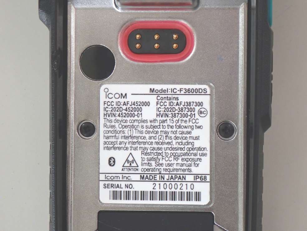
AFJ452000
Jun 02, 2026VHF DIGITAL TRANSCEIVER
Equipment Class
TNF - Licensed Non-Broadcast Transmitter Held to Face
AFJ452100
May 12, 2026UHF DIGITAL TRANSCEIVER
Equipment Class
TNF - Licensed Non-Broadcast Transmitter Held to Face
AFJ444500
Sep 12, 2024Scanning Receiver
Equipment Class
CSR - Scanning Receiver
AFJ410900
Jul 09, 2024Linear Amplifier
Equipment Class
AMP - Amplifier