AFJIC-706MK2GReceiver portion of amateur transceiver
ICOM Incorporated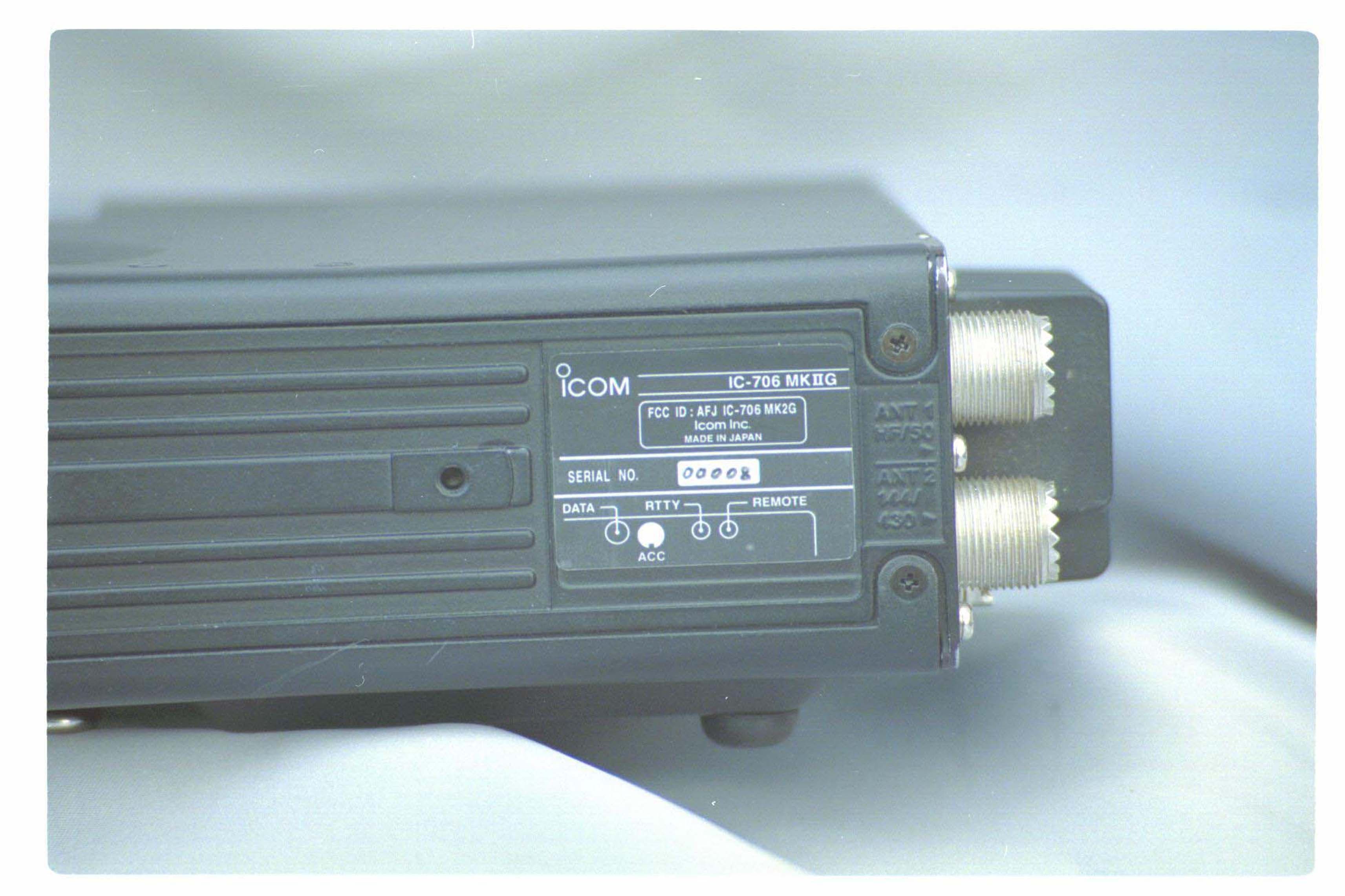
Click to zoom
Application Details
- Equipment Class
- CSR - Scanning Receiver
- Date of Grant
- Mar 11, 1999
- Application Purpose
- Original Equipment
- Date of Application
- Jan 10, 1999
- Equipment Note
- Receiver portion of amateur transceiver
- Frequency Range
- 400.00000000 - 470.00000000
- Company
- ICOM Incorporated
- Country
- Japan
Documents & Files
Document Text
Text extracted from the exhibit documents filed with the FCC. Open a document above to read the original.
Users Manual
INSTRUCTION MANUAL i706MK™G HF/VHF/UHF ALL MODE TRANSCEIVER This device complies with Part 15 of the FCC rules. Operation is sub- ject to the following two conditions: (1)This device may not cause harmful interference, and (2)this device must accept any interference received, including interference that may cause undesired operation. EXPLICIT DEFINITIONS PRECAUTIONS IMPORTANT Read this instruction manual carefully before attempting to operate the transceiver. Save this instruction manual. This instruction manual contains important safety and operating instructions for the IC-706MKIIG. RWARNING HIGH VOLTAGE! NEVER attach an antenna or internal antenna connector dur- ing transmission. This may result in an electrical shock or burn. RNEVERapply AC to the [DC13.8V] socket on the transceiver rear panel. This could cause a fire or ruin the transceiver. RNEVERapply more than 16 V DC, such as a 24 V battery, to the [DC13.8V] socket on the transceiver rear panel. This could cause a fire or ruin the trans- ceiver. RNEVERlet metal, wire or other objects touch any internal part or connectors on the rear panel of the transceiver. This will cause electric shock. RNEVERexpose the transceiver to rain, snow or any liquids. NEVER allow children to play with the transceiver. AVOID using or placing the transceiver in areas with temperatures below –10°C (+14°F) or above +60°C (+140°F). Be aware that temperatures on a vehicle’s dashboard can exceed 80°C, resulting in permanent damage to the transceiver’s front panel if left there for extended periods. AVOID placing the transceiver in excessively dusty environments or in direct sunlight. AVOID placing the transceiver against walls or putting anything on top of the transceiver. This will obstruct heat dissipation. During mobile operation, DO NOToperate the trans- ceiver without running the vehicle’s engine. When transceiver power is ON and your vehicle’s engine is OFF, the vehicle’s battery will soon become exhausted. Make sure the transceiver power is OFF before start- ing the vehicle. This will avoid possible damage to the transceiver by ignition voltage spikes. During maritime mobile operation, keep the transceiv- er and microphone as far away as possible from the magnetic navigation compass to prevent erroneous indications. BE CAREFUL! The heatsink will become hot when operating the transceiver continuously for long periods. BE CAREFUL!If a linear amplifier is connected, set the transceiver’s RF output power to less than the lin- ear amplifier’s maximum input level, otherwise, the lin- ear amplifier will be damaged. Use Icom microphones only (supplied or optional). Other manufacturer’s microphones have different pin assignments and connection to the IC-706MKIIG may damage the transceiver. Beat signals may be heard on some frequencies. These will occur as a result of circuit construction. For U.S.A. only Caution:Changes or modifications to this transceiver, not expressly approved by Icom Inc., could void your author- ity to operate this transceiver under FCC regulations. The explicit definitions described below apply to this instruction manual. The IC-706MKIIG Europe version complies with essential requirements of the 89/336/EEC direc- tive for Electromagnetic Compatibility under the conditions listed below. This compliance is based on confor- mity with the European harmonized standard ETS300 684 Jan. 1997 (EMC product standard for Commercially Available Amateur Radio Equipment). Condition: •In combination with PS-85 •When connected to a power supply via OPC-639 WORDDEFINITION RWARNING Personal injury, fire hazard or electric shock may occur. CAUTION Equipment damage may occur. NOTE If disregarded, inconvenience only. No risk of personal injury, fire or electric shock. TABLE OF CONTENTS IMPORTANT.............................................................i PRECAUTIONS........................................................i EXPLICIT DEFINITIONS..........................................i TABLE OF CONTENTS............................................ii UNPACKING.............................................................ii 1PANEL DESCRIPTION.....................................1–8 nFront panel...............................................................1 nFunction switches.....................................................3 nRear and side panels...............................................5 nFunction display.......................................................7 nMicrophone (HM-103)...............................................8 2INSTALLATION AND CONNECTIONS..........9–14 nUnpacking.................................................................9 nGrounding.................................................................9 nAntenna....................................................................9 nInstallation................................................................10 nRequired connections...............................................11 nAdvanced connections.............................................12 nPower supply connections........................................13 nExternal antenna tuners and linear amplifier............14 3FREQUENCY SETTING................................15–19 nWhen first applying power (CPU resetting)..............15 nInitial settings............................................................15 nVFO description........................................................16 nFrequency setting.....................................................17 nMode selection.........................................................19 4RECEIVE AND TRANSMIT..........................20–37 nFunctions for receive................................................20 nFunctions for transmit...............................................24 nSplit frequency operation..........................................28 nTone squelch operation............................................30 nTone scan operation...............................................…
Text truncated - open the document above for the full version.
Attestation Statements
0 ICOM” lcom America, Inc Corporate Headquarters 2380 116th Ave. N.E. Bellevue, Washlngton 98004 Phone: (425) 454-8155 Fax: (425) 454-1509 Customer Service: (425) 454-7619 January 19,1999 Federal Communications Commission EQUIPMENT APPROVAL SERVICES PO Box 358315 Pittsburgh, PA 15251-3315 Attention: Authorization & Evaluation Division Applicant: ICOM INCORPORATED Equipment: FCC ID: AFJIC-706MK2G FCC Rules: Part 15.37 (B) (New) Gentlemen: On behalf of the Applicant, enclosed please find the Application Form, Test Data Report and all pertinent documentation, the whole for certification of the referenced equipment as shown. Filing fees are attached to the Fee Processing Form. Should you need any further information, kindly contact the writer who is authorized to act for the Applicant. Best regards A I Masaaki Takahashi Manager, New Product Development MT: sg Enclosures First in Communications C/l,jAE4 S,~,L.tSiS~~!‘!‘.~!“L c--,’ ; Ci-; v L- -I 3071 - #5 Road, Unit 9, Richmond, B.C., Canada V6X 2T4 (604) 273-7400 FAX (604) 273-l 900 (corn America, Inc, Corporate Headquarters 2380 116th Ave. N.E. Bellevue, Washington 98004 Phone: (425) 454-8155 Fax: (425) 454-l 509 Customer Service: (425) 454-7619 0 lCOM@ January 19, 1999 Federal Communications Commission Authorization & Evaluation Division 7435 Oakland Mills Road Columbia, Maryland 21046 Gentlemen: This is to advise that we are in full compliance with the Anti-Drug Abuse Act. The Applicant is not subject to a denial of federal benefits pursuant to Section 5301 of the Anti-Drug Abuse Act of 1988, 12 USC 862, and no party to the application is subject to a denial of federal benefits pursuant to that section. Sincerely, ICOM America, Inc. /g& 9 Masaaki Takahashi Manager, New Product Development First in Communications ;, :::?u A G +I . . , L i.: j i. I ; ..- 3071 - #5 Road, Unit 9, Richmond, B.C., Canada V6X 2T4 (604) 273-7400 FAX (604) 273-1900 0 ICOM” lcom America, Inc. Corporate Headquarters 2380 116th Ave. N.E. Bellevue, Washington 98004 Phone: (425) 454-8155 Fax: (425) 454-l 509 Customer Service: (425) 454-7619 Application for Equipment Certification FCC Identifier AFJ-IC-706MK2G January 19, 1999 Scanning Receiver Statement for Compbnce with 5 2.1033 (b) (12) The equipment under application herein incorporates a scanning receiver. Accordingly, 15.121 of the Commission’s rules applies. The equipment under application herein is incapable of operating (tuning), or being readily altered by the user to operate within the frequency bands allocated to the Domestic Public cellular Radio Telecommunications Service (“Cellular Radio Service”). The equipment is also incapable of converting digital cellular transmissions to analog voice audio. The receiver portion of the equipment under application herein scans bands 0.03-200MHz and 400-470MHz, and the receiver does not scan the bands used by the Cellular Radio Service, 824-849 and 869-894MHz. The receiver portion of the equipment under application cannot be altered to enable it to scan the Cellular Radio Service bands by means of clipping the leads of or installing a diode, resistor and/or jumper wire, or other such simple component. Nor can the receiver be made to scan the Cellular Radio Service bans by replacing a plug-in semiconductor chip, since no such plug-in chips are utilized. The semiconductor chips that are utilized in the equipment cannot be , erased and reprogrammed. The equipment has no circuitry capable of connecting any digital signals into analog voice audio. In view of the above, the equipment complies with 5 15.121 of the Commission rules. Sincerely yours, ICOM Incorporated Masaaki Takahashi Manager, New Product Development First in Communications CANADA SALES/SERVICE OFFICE 3071 - #5 Road, Unit 9, Richmond, B.C., Canada V6X 2T4 (604) 273-7400 FAX (604) 273-1900
Block Diagram
D10 1SS375D9 1SS375 ANT SW RFSW NJM2904MNJM2904M PWR /SWRDET HFORHREF IC1BIC1A 0.03~ 2.0MHz 2.0~ 4.0MHz 4.0~ 8.0MHz RL1AG201344 Q92SC4213 B HPAO Q161MRF1508 Q172SRFJ7044 Q171 SRFJ7044 DRIVER(a) FILTER UNIT PA UNIT 1.6MHz 1.6MHz IC231UPC2709T 60MHz 10dB Q1012SK2854 Q121MXR9745RT1 HF/ 50MHz 20dB Q121 DTC114EEQ122 DTA114EE Q111 DTC114EEQ112 DTC114EE HPF BOARD UPC1658G PR1S 40MHz 0.1-2MHz30-40MHz 2-4MHz4-8MHz IC1511LO 3dB 3dB 3dB AGCALC D271HSB88WS 70.7MHz IC281 3dB 69.0115MHz FI511FL-261 3dB R8VT8V UPC2709T AGCALC D551 HSB88WS 69-71MHz IC521UPC1688 3dB 9.0115MHz FI561FL-23 10.7MHz 2LO T8VR8V ATT D522ATT D522 ATT D521 ATT D521 AGC UPC2713T TX TOTAL GAIN ALC CTRL D561 MA862D562 MA862 Q636DTA114EE IC571 WAVE Q572 2SC4081 R579 RV-143 R8V UL ATT D572ATT D572 WFMDET NBS MAIN UNIT IC631LA1150N D6321SS375 Q634 2SC4081Q635 DTC114EE DRIVE CTRL Q5732SC4081 DRIV IC861BU4052BCFV OPT UT-102 BEEP IC891ANJM2902V R900RV-150 IC891BNJM2902V DATA WCNT WFAF X1 CSB800J 0.8MHz TA4101F 2SK882 3SK126 2SK882 AGCCTRL 2SK882 2SC4081 2SA1576 2SC4081 FI601 FI611 Q611 Q621 GAINCONTROL Q632 Q631 R623RV-148 Q731 Q741 Q751 IC841 SFECV10.7MA-5 SFECV10.7MA-5 2SC4081 Q601 FL-272FI671 Q721 2SC4081 22-30MHz8-15MHz15-22MHz 40-60MHz(TX or RX/PREAMP OFF)40-60MHz(PREAMP ON) Q1912SK2171 4 IC221TA4001F 144MHz 145MHz 3dB Q211MRF1508 Q231SRFJ7044 144/430MHz Q301 DTC114EUQ351 DTC114EUD343 1SS355 Q402 DTC114EUQ403 3SK291 D311 UM9401FD342 UM9401FD341 UM9401FD344 UM9401F DRIVER(b) 8.0~ 15.0MHz 15.0~ 22.0MHz 22.0~ 30.0MHz 30.0~ 60.0MHz D261 MI407D293 1SS355 PWRDET D262 MS742D263 MA742VFOR PWRDET UFORD312 MA742D313 MA742 144MHz430MHz FAN D291 UM9401FD292 UM9401F D171 DAN202UD172 DAN202U ANT1 HF/50MHz ANT2 144/430MHz SP UNIT RX FREQ=0.03-29.999999MHz 1LO FREQ:(DISP. FREQ)+(69.0115MHz) 144MHz430MHz D574 MA8056 MQ571 2SB1132 RQ572 2SC4081 R 14V HV RL591 JV-12-KTQ591 DTC114EE from PS CHASSIS F591FGB 4A D451 1SV308D452 1SV308D401 1SV308D402 1SV308 D573 DAN202UD575 DAN202U VURX Q351 2SC4213D361 1SV304Q381 2SC4213 VCO2VCO3 Q102SC4405 Q452 DTC114EUD453 1SV305D455 1SV305Q453 3SK291 D454 1SV305D456 1SV305 D403 MA2SV05 D406 MA2SV05 Q331 2SK508Q361 2Sk508 D407 MA357D410 MA2SV05 D408 MA357D409 MA2SV05 RIPPLE FIL 8V Q3622SC4116 RIPPLE FIL Q3912SC4116 IC222TA4002F FI371,FI372,FI373 LFSC25N12B 0440B 430MHz OPTION FM OPTION FILTER-2FILTER-1 FL-94 2SC4081 AGCSML FI681 SSB/CW/RTTY AM/FM-N Q776 Q777 2SA1576 DET AM DET AGC HREFHFOR EALCALC VFOR TA31136FN NJM2902V NJM2902V NJM2902VNJM2902V FM 2SA1576 LEVELSHIFT RFGC RX TOTAL GAIN D771 1SS375 RFGCTRL IC791 R741 RV-148 D7611SS375 3kHz Q771 2SC4081 D772 AGFSAFMS DELAY CTRL Q772 UMC1NQ773 UMC1N MA2S111 Q7742SC4081 IC811B FI791SFPC455E DE-IC811ANJM2902V POCVUFORVREF IC1091BIC1091C IC1091A ALCL Q1131 D1131 MA8036 L D1132 DAP222 EMPH BFO OVDV 2SC4081Q1092 SW MODE SW UPC5023-077 250Hz IC811D NJM2902VIC811C NJM2902V CTCV SQL 3kHz IC891CNJM2902V R896EVN-D2AA03B25 IC931 9600 DATA IN COMPA- RATOR 9600 DATA OUT IC981DNJM2058M IC981CNJM2058M COMSMIGV SSAFAMAFFMAF AMOD BU4052BCFVIC1141B SW BU4052BCFVIC1141A VCA 2SC4081Q961 COMP GAINR945EVN-D2AA03B25 AFO ETON TONE PD LOOP FILTER FM AM SSB/AM ICHICL 1/N NJM2902V LC7153M 2SC4081 5.006KHz UREF IC1091D IC1041NJM1496V AMS8 Q1041DTC114EE CW/RTTY IC971 TC4W53FU IC981BNJM2058M PRE-LIMITIC981ANJM2058M Q1013 T8V IC1011 9.0115MHz D1014 1SS375D1013 1SS375D1012 MA357Q1011 2SK210 EMPH/ KDS8 WAVE FORM Q161 P/D 1/R DIV 1/N DIV IC461N DATA MLLV Q4912SK880 UN-LOCKUN-LOCK UL Q261 DTC114EE LMX2306 Q461 DTA144EUD261 DAN222 Q512SC4081 DDS P/D LOOP FIL Q1 2SK210D1 MA357 Q212SC4081 Q352 DTA144EUQ322 DTA144EUQ321 2SC4213 D531 UPC2710 VCO1 IC541 MA717WK D331 KV1470D301 KV1470Q301 2SK508 RX FREQ=30-59.999999MHz FILSELECT RX FREQ=129-143.999999MHzRX FREQ=144-148MHzRX FREQ=60-128.999999MHzRX FREQ=400-470MHzRX FREQ=148.000001 -199.999999MHz Q141 DTA114EUQ142 DTA114EUQ143 DTA114EUQ144 DTA114EUQ145 DTA114EUQ851 DTA114EU OPTCR-282 Q621 2SC4403D601 MA357R602 RV-150 X621CR-275A (30.000000MHz) Q6612SC4403Q931 2SC4081 FSKK FI71 Q71 2SC4081 IC101SC-1246 (30.000000MHz) D931 MA2S111 SFECV10.5MA-5 Q232 DTC114EU Q6812SC4403 N DATA DDS IC901SC-1287 Q9412SC4403 BFO N DATA 2SC4403 2LO(60.000000MHz) SPS RL231 SY-12-K AAF VCA AFGC OPT UT-106 DATA IC201 M5282 HV 14V H5V 5V8V IC291 TA7805FIC281 TA7808S IC271 TA78L05F AFO (FRONT PHONE) IC231LA4425A BFO X1 CR-606 15.99MHz X2 CR-605 39.98MHz SUBCPU 5V 1/R N DATA RESET S-80945ALMP IC4 IC1HD6433834H 8V WAVE FORMCTRL MAIN DIALSUB DIAL (9.8304MHz) X1 LCD DRIVER LCD IC2 SED1522F0C DS4 IC3BU4030BG IC5 S81250PG-PDQ10 2SC4081 RQ11 2SB1143 SD9 MA2S111 KEYLIGHT KEY DIMMER CTRL KEY MA-406 Q14 2SC4081 RQ13 2SC1132 R EEPROM DRESKDS DOTDASHCTCVVOXLAVXL MAIN CPU UL IC2001HD64F3337Y IC2121IC2122B TC7W04FU X2161CR-636(14.7456MHz) X25650S8I-2.5 CI-V I/F D/A EXPAND N DATA HV RESET DATA IC2122C TC7W04FU IC2161 S-80942ANMP-DD6 IC2201M62352GP IC2221 BU4094BCFVIC2222 BU4094BCFVIC2232 BU4094BCFV TUNER CTRL IC2131 TC4S81FQ2131 DTC114EED2133 DAN222 IC351IC2241 TD62783AF Q2221 UMC3NQ2222 UMC3NQ2223 UMC3NQ2224 UMC3NQ2225 UMC3N IC2202NJM2902V Q2171 2SA1576 Q2172 2SC4081 IC2231 TC74HC4094AF TD62783AFN EEPROM IC6X24C01S-2.7-T FRONT UNIT AFRF/SQLSHIFT LED DRIVER LEDPTT DRIVER VR BOARD Q4 2SD1619 TQ9 DTA114EE DISPLAY BOARD DIMMER CTRL BACKLIGHT PTT DS5 D2264 Q2 2SB1132 R Q8 XP4111Q12 XP4111Q15 DTA114EE Q3 2SC4081 R RXTXCOMMON DATE MODEL DWN.NO. Icom Inc. PLL UNIT BLOCK DIAGRAM -5B1 ’98.11.27 IC-706MK2G
Cover Letter(s)
0 ICOM” lcom America, Inc Corporate Headquarters 2380 116th Ave. N.E. Bellevue, Washlngton 98004 Phone: (425) 454-8155 Fax: (425) 454-1509 Customer Service: (425) 454-7619 January 19,1999 Federal Communications Commission EQUIPMENT APPROVAL SERVICES PO Box 358315 Pittsburgh, PA 15251-3315 Attention: Authorization & Evaluation Division Applicant: ICOM INCORPORATED Equipment: FCC ID: AFJIC-706MK2G FCC Rules: Part 15.37 (B) (New) Gentlemen: On behalf of the Applicant, enclosed please find the Application Form, Test Data Report and all pertinent documentation, the whole for certification of the referenced equipment as shown. Filing fees are attached to the Fee Processing Form. Should you need any further information, kindly contact the writer who is authorized to act for the Applicant. Best regards A I Masaaki Takahashi Manager, New Product Development MT: sg Enclosures First in Communications C/l,jAE4 S,~,L.tSiS~~!‘!‘.~!“L c--,’ ; Ci-; v L- -I 3071 - #5 Road, Unit 9, Richmond, B.C., Canada V6X 2T4 (604) 273-7400 FAX (604) 273-l 900 (corn America, Inc, Corporate Headquarters 2380 116th Ave. N.E. Bellevue, Washington 98004 Phone: (425) 454-8155 Fax: (425) 454-l 509 Customer Service: (425) 454-7619 0 lCOM@ January 19, 1999 Federal Communications Commission Authorization & Evaluation Division 7435 Oakland Mills Road Columbia, Maryland 21046 Gentlemen: This is to advise that we are in full compliance with the Anti-Drug Abuse Act. The Applicant is not subject to a denial of federal benefits pursuant to Section 5301 of the Anti-Drug Abuse Act of 1988, 12 USC 862, and no party to the application is subject to a denial of federal benefits pursuant to that section. Sincerely, ICOM America, Inc. /g& 9 Masaaki Takahashi Manager, New Product Development First in Communications ;, :::?u A G +I . . , L i.: j i. I ; ..- 3071 - #5 Road, Unit 9, Richmond, B.C., Canada V6X 2T4 (604) 273-7400 FAX (604) 273-1900 0 ICOM” lcom America, Inc. Corporate Headquarters 2380 116th Ave. N.E. Bellevue, Washington 98004 Phone: (425) 454-8155 Fax: (425) 454-l 509 Customer Service: (425) 454-7619 Application for Equipment Certification FCC Identifier AFJ-IC-706MK2G January 19, 1999 Scanning Receiver Statement for Compbnce with 5 2.1033 (b) (12) The equipment under application herein incorporates a scanning receiver. Accordingly, 15.121 of the Commission’s rules applies. The equipment under application herein is incapable of operating (tuning), or being readily altered by the user to operate within the frequency bands allocated to the Domestic Public cellular Radio Telecommunications Service (“Cellular Radio Service”). The equipment is also incapable of converting digital cellular transmissions to analog voice audio. The receiver portion of the equipment under application herein scans bands 0.03-200MHz and 400-470MHz, and the receiver does not scan the bands used by the Cellular Radio Service, 824-849 and 869-894MHz. The receiver portion of the equipment under application cannot be altered to enable it to scan the Cellular Radio Service bands by means of clipping the leads of or installing a diode, resistor and/or jumper wire, or other such simple component. Nor can the receiver be made to scan the Cellular Radio Service bans by replacing a plug-in semiconductor chip, since no such plug-in chips are utilized. The semiconductor chips that are utilized in the equipment cannot be , erased and reprogrammed. The equipment has no circuitry capable of connecting any digital signals into analog voice audio. In view of the above, the equipment complies with 5 15.121 of the Commission rules. Sincerely yours, ICOM Incorporated Masaaki Takahashi Manager, New Product Development First in Communications CANADA SALES/SERVICE OFFICE 3071 - #5 Road, Unit 9, Richmond, B.C., Canada V6X 2T4 (604) 273-7400 FAX (604) 273-1900
Operational Description
1 RECEIVER CIRCUITS 1-1 HF/50 MHz RF CIRCUIT (FILTER, MAIN AND HPF BOARDS) HF/50 MHz RF filters pass only the desired band signals and suppress any undesired band signals. The HF/50 MHz RF circuit has 7 low-pass filters and 7 high-pass filters for specified band use. HF/50 MHz RF signals from the [ANT1] connector, pass through one of 7 low-pass filters as below, the transmit/ receive switching relay (FILTER unit; RL1) and low-pass filter (FILTER unit; L1, L2, C1-C5), and are then applied to the MAIN board via J1 (FILTER unit). The signals from the FILTER board are applied to or bypass the 20 dB attenuator (R122, R125, R126). The signals pass through the high-pass filter (L132, L133, C132-C137) to suppress strong signals below 1.6 MHz and are then applied to the HPF board via the “TOAT” terminal. (1) 0.03-2 MHz and 30-40 MHz The signals pass through a low-pass filter (L101, L102, C101-C105), and then applied to the preamplifier circuit on the MAIN board. (2) 2-30 MHz The signals from the low-pass filter (L101, L102, C101-C105) are applied to one of 6 high-pass filters as at right above and are then applied to the preamplifier circuit on the MAIN board. (3) 40-60 MHz The signals pass through the low-pass filter (L172, L173, C172-C176) and the high-pass filter (L174, L175, C177-C181) via D171 and are then applied to the preamplifier circuit on the MAIN board. 1-2 VHF AND UHF RF CIRCUIT (PA UNIT) The VHF and UHF RF circuit passes and amplifies only the desired band signals and suppresses any undesired band signals. The VHF RF circuit has a preamplifier and band-pass filters. The VHF RF signals from the [ANT2] connector pass through the low-pass filter (L263, L264, L265, C274-C277) and antenna switching circuit (D261, D291, D292, D293). The signals are amplified at the preamplifier circuit (Q403) between the band-pass filters (D406, D407 and D410). The UHF RF signals from the [ANT2] connector pass through the high-pass filter (L316, L317, C326- C327), pass through the low-pass filter (L314, L315, C322-C325) and antenna switching circuit (D341, D342, D343). The signals are amplified at the preamplifier circuit (Q453) between the band-pass filters (D454, D456). The filtered signals are applied to the MAIN board via J481 (PA unit) and are then applied to the preamplifier circuit. 1-3 PREAMPLIFIER CIRCUIT (MAIN BOARD) The preamplifier circuit in the IC-706MKIIG has approx. 15dB gain over a wide-band frequency range. When the preamplifier is turned ON, the signals from the RF circuit are applied to the preamplifier (IC151) via D2182. Amplified or bypassed signals are applied to the 1st mixer circuit (D271). 1-4 1ST MIXER CIRCUIT (MAIN BOARD) The 1st mixer circuit mixes the receive signals with the 1st LO signal to convert the receive signal frequencies to a 69 or 70.7 MHz 1st IF. The signals from the preamplifier circuit, or signals which bypass the preamplifier, are applied to a low- pass filter and then to the 1st mixer (D271). The 1st LO signals (69.0415-539.0115 MHz) enter the MAIN board from the PLL unit via J281. The LO signal is amplified at IC-281, filtered by a low-pass filter, and then, applied to the 1st mixer. 1-5 1ST IF CIRCUIT (MAIN BOARD) The 1st IF circuit filters and amplifies the 1st IF signals. The 1st IF signals are applied to a Crystal Filter (FI511) to suppress out-of-band signals. The 69 MHz 1st IF signals (except WFM) pass through the crystal filter (FI511), however, the 70.7 MHz 1st IF signal (WFM) passes through a band-pass filter (L501-L504, C501-C506). Then the filtered signals are applied to the IF amplifier (IC281). The AGC voltage is supplied to the transmit/receive switching circuit (D521, D522) and D521/D522 function as PIN attenuators for AGC operation. The amplified signals are then applied to the 2nd mixer circuit (D551) via the band-pass filter (L542-L546, C542-C545). 1-6 2ND MIXER CIRCUIT (MAIN BOARD) The 2nd mixer circuit mixes the 1st IF signals and 2nd LO signal (60.00 MHz) to convert the 1st IF to a 2nd IF. The 1st IF signals from the band pass filter (L542-L546, C542-C545) are converted to 9 MHz or 10.7 MHz 2nd IF signals at the 2nd mixer (D551). The 2nd IF signals are applied to the band-pass filter (FI561) to suppress undesired signals, such as the 2nd LO signal, and are then applied to the noise blanker gate (D561, D562). While in WFM mode, the IF signals pass through the low-pass filter (L601, C601-C603), IF amplifier (Q601), ceramic filter (FI611) and IF amplifier (Q611). The signals are then applied to the WFM demodulator circuit (IC631). 1-7 NOISE BLANKER CIRCUIT (MAIN BOARD) The noise blanker circuit detects pulse type noise, and turns OFF the signal line when noise appears. A portion of the signals from FI561 are amplified at the noise amplifiers (Q621, Q638, amplifier section of IC631), then detected at the noise detector (D632) to convert the noise components to DC voltages. The converted voltages are then applied to the noise blanker switch (Q634, Q635). At the moment the detected voltage exceeds Q634’s threshold level, Q635 outputs a blanking signal to close the noise blanker gate (D561, D562) by applying reverse-biased voltage. The detected voltage from D632 is also applied to the noise blanker AGC circuit (Q631, Q633) and is then fed back to the noise amplifier (IC631) as a bias voltage. The noise AGC circuit prevents closure of the noise blanker gate for long periods by non-pulse-type noise. The time constant of the noise blanker AGC circuit is determined by R637. The 2nd IF signals from the noise blanker gate are then applied to the 2nd IF circuit. 1-8 2ND IF CIRCUIT The 2nd IF circuit amplifies and filters the 2nd IF signals. The 2nd IF signals from the noise blanker gate (D561, D562) are amplified at the IF amplifier (IC571) via the Tx/Rx switch (D572) and applied to a 2nd IF filter as shown below. The filtered or bypassed signals are applied to the buffer amplifier (Q721), IF amplifiers (Q731, Q741) and buffer amplifier (Q751) to obtai…
Text truncated - open the document above for the full version.
Parts List/Tune Up Info
IC-706MKIIG Alignment Procedure * Front Board RIT/SHIFT knob alignment - Hold both “P.AMP/ATT” and “RIT” buttons, and turns radio on. (The radio should indicate “SHIFT-ADJ” on LCD display) - Set “SHIFT” knob to center - Repress “MENU” button for more than 2 seconds. (The radio should show “Good” on the display) * PLL Board Reference oscillator - Set L623 to center - Connect RF volt meter to P681 - Adjust L681 and L682 for maximum level - Set frequency counter to P681 - Adjust L601 for 60.000000MHz (If L601 is outside of alignment range, align R60 and L36 as well) - Verify P681 output level for more than 0dBm LPL lock voltage - Set display to 0.03MHz and USB - Connect multi-meter to CP131 - Adjust C4 for 2V VCO1 lock voltage - Set display to 128.99999MHz and USB - Connect multi-meter to CP401 - Adjust C306 for 4V VCO2 lock voltage - Set display to 199.99999MHz and USB - Connect multi-meter to CP401 - Adjust C335 for 4V VCO3 lock voltage - Set display to 470.00000MHz and USB - Connect multi-meter to CP401 - Adjust C367 for 4V 1st LO - Set display to 0.03MHz - Connect RF volt meter to P891 - Verify output voltage for more than –15dBm - Set display to 29.99999MHz - Connect RF volt meter to P891 - Verify output voltage for more than –15dBm - Set display to 30.00000MHz - Connect RF volt meter to P891 - Verify output voltage for more than –15dBm - Set display to 59.99999MHz - Connect RF volt meter to P891 - Verify output voltage for more than –15dBm - Set display to 60.00000MHz - Connect RF volt meter to P891 - Verify output voltage for more than –15dBm - Set display to 128.99999MHz - Connect RF volt meter to P891 - Verify output voltage for more than –15dBm - Set display to 129.00000MHz - Connect RF volt meter to P891 - Verify output voltage for more than –15dBm - Set display to 144.00000MHz - Connect RF volt meter to P891 - Verify output voltage for more than –15dBm - Set display to 146.00000MHz - Connect RF volt meter to P891 - Verify output voltage for more than –15dBm - Set display to 148.00000MHz - Connect RF volt meter to P891 - Verify output voltage for more than –15dBm - Set display to 430.00000MHz - Connect RF volt meter to P891 - Verify output voltage for more than –15dBm - Set display to 440.00000MHz - Connect RF volt meter to P891 - Verify output voltage for more than –15dBm - Set display to 450.00000MHz - Connect RF volt meter to P891 - Verify output voltage for more than –15dBm BFO - Connect frequency counter to P991 - Receive FM signals - Verify P991 output frequency for 9.4665MHz - Connect RF volt meter to P991 - Verify P991 output signal for more than –20dBm * Main Board Transmitter Alignment - Set R945 and R896 for center - Set R1225 to 90 degrees position - Set display to 14.10000Mhz, USB, high power and mic gain 5 - Connect RF power meter to antenna connector (ANT1) - Connect AF signal generator to mic connector - Apply 1.5KHz/3mV signals to mic connector - Transmit - Adjust L566, L563, L562, L512 and L511 for maximum level. - Set display to 52.00000Mhz, USB, high power and mic gain 5 - Connect RF power meter to antenna connector(ANT1) - Connect AF signal generator to mic connector - Apply 1.5KHz/3mV signals to mic connector - Transmit - Adjust R579 for 50W - Set display to 14.10000Mhz, USB, high power and mic gain 5 - Connect RF power meter to antenna connector(ANT1) - Connect AF signal generator to mic connector - Apply 1.5KHz/30mV signals to mic connector - Transmit - Adjust R1082 for 105.0W - Set display to 52.00000Mhz, USB, high power and mic gain 5 - Connect RF power meter to antenna connector (ANT1) - Connect AF signal generator to mic connector - Apply 1.5KHz/30mV signals to mic connector - Transmit - Adjust R1084 for 100W - Set display to 145.00000Mhz, USB, high power and mic gain 5 - Connect RF power meter to antenna connector (ANT2) - Connect AF signal generator to mic connector - Apply 1.5KHz/30mV signals to mic connector - Transmit - Adjust R1086 for 50W - Set display to 435.00000Mhz, USB, high power and mic gain 5 - Connect RF power meter to antenna connector (ANT2) - Connect AF signal generator to mic connector - Apply 1.5KHz/30mV signals to mic connector - Transmit - Adjust R1088 for 21W Carrier Suppression - Set display to 14.10000Mhz, USB, high power and mic gain 5 - Connect Spectrum analyzer to antenna connector - Connect AF signal generator to mic connector - Apply no signals to mic connector - Transmit - Adjust R1045 for minimum level on both USB and LSB FM VCO - Set display to 29.10000Mhz, FM, Tone off, high power and mic gain 5 - Connect RF power meter to antenna connector - Connect Multi-meter to CP1011 - Apply no signals to mic connector - Transmit - Adjust C1022 for 1.8V FM Transmit Modulation - Set display to 29.10000Mhz, FM, Tone off, high power and mic gain 5 - Connect deviation meter to antenna connector - Connect AF signal generator to mic connector - Apply 1KHz/30mV signals to mic connector - Transmit - Adjust CR1…
Text truncated - open the document above for the full version.
Contact Information
Applicant
Atsushi Tomiyama(General Manager)
Technical Contact
Icom America IncMasaaki Takahashi
[email protected](425) 454-8155
2380 116th Ave NE · Bellevue, Washington · United States
Non-Technical Contact
Icom America IncMasaaki Takahashi
[email protected](425) 454-8155
Test Firm
Japan Quality Assurance Org.Katsumi Nishii
Technical Specifications
| # | Rule Parts | Frequency Range | Power Output | Tolerance |
|---|---|---|---|---|
| 2 | 15B | 400 MHz - 470 MHz | - | % |
Other Applications from ICOM Incorporated
AFJ453700
Jul 23, 2026Mobile Transceiver
Equipment Class
DTS - Digital Transmission System
AFJ452000
Jun 02, 2026VHF DIGITAL TRANSCEIVER
Equipment Class
TNF - Licensed Non-Broadcast Transmitter Held to Face
AFJ452100
May 12, 2026UHF DIGITAL TRANSCEIVER
Equipment Class
TNF - Licensed Non-Broadcast Transmitter Held to Face
AFJ444500
Sep 12, 2024Scanning Receiver
Equipment Class
CSR - Scanning Receiver
AFJ410900
Jul 09, 2024Linear Amplifier
Equipment Class
AMP - Amplifier