AFJIC-F4TR-1UHF-FM Hand Held Transceiver
ICOM Incorporated
Click to zoom
Application Details
- Equipment Class
- TNF - Licensed Non-Broadcast Transmitter Held to Face
- Date of Grant
- Mar 05, 2000
- Application Purpose
- Original Equipment
- Date of Application
- Jan 12, 2000
- Equipment Note
- UHF-FM Hand Held Transceiver
- Frequency Range
- 450.00000000 - 490.00000000
- Company
- ICOM Incorporated
- Country
- Japan
Documents & Files
Document Text
Text extracted from the exhibit documents filed with the FCC. Open a document above to read the original.
Users Manual
INSTRUCTION MANUAL This device complies with Part 15 ofthe FCC Rules. Operation is subject tothe condition that this device does notcause harmful interference. iF4TRUHF TRUNKED RADIO Count on us! 6-9-16 Kamihigashi, Hirano-ku, Osaka 547-0002 Japan A-5632?-1USPrinted in Japan© 1999 Icom Inc. 4 SPECIFICATIONS AND OPTIONS 4-1 Specifications• GENERALFrequency coverage (MHz) : 400–430, 450–490, 480–512 Mode : 16K0F3E (25 kHz) 11K0F3E (12.5 kHz) Usable temperature range : –30 ̊C to +60 ̊C; –22°F to +140°F Dimensions (proj not incl.) : 57(W) × 140(H) × 37 (D) mm ; 2 1 ⁄ 4 (W) × 5 1 ⁄ 2 (H) × 1 15 ⁄ 32 (D) in Weight (with BP-196) : 390 g; 13.8 oz • TRANSMITTEROutput power : 4 W • RECEIVERSensitivity (12 dB SINAD) : 0.3 μV Intermodulation rejection ratio : 75 dB typ. Spurious response rejection : 70 dB typ.Adjacent channel selectivity : 70 dB typ. (25 kHz) 65 dB typ. (12.5 kHz) Audio output power : 500 mW (at 5% distortion with an 8 Ω load) 4-2 Options• HM-46/HM-54/HM-75A SPEAKER-MICROPHONES Combination speaker-microphone that provides convenient opera-tion while hanging the transceiver from your belt clip. • BC-119 DESKTOP CHARGER + AD-81 CHARGER ADAPTER Used for rapid charging of battery packs. Charging time: 1.5 to 2hours. An AC adapter is supplied with the chargers (depending onversion). • BC-121 MULTI-CHARGER + AD-81 CHARGER ADAPTER + BC-124 AC ADAPTER Rapidly charges of up to 6 battery packs (six AD-81’s are required)at once. Charging time: 1.5 to 2 hours. • BC-133 DESKTOP CHARGER Regularly charges battery pack with/without transceiver. The ACadapter, BC-122, is additionally required. Charging time: approx. 15hours • BC-110A/D/V WALL CHARGER Used for charging via a domestic AC wall socket. •CP-12L CIGARETTE LIGHTER CABLE Used for charging via a vehicle’s cigarette lighter socket (12 V). •OPC-254L DC POWER CABLE Used for charging with an external power supply. •BP-194 BATTERY CASE Takes eight (8) AA (R6) size batteries. External DC-jack on thetransceiver can be used to charge the Ni-Cd battery cells. •SP-13 EARPHONE Provides clear audio in noisy environments. All stated specifications are subject to change without notice orobligation. IMPORTANTREAD ALL INSTRUCTIONS carefully and completely before using the transceiver.SAVE THIS INSTRUCTION MANUAL. This manual contains important safety and operating instructions for the IC-F4TR . EXPLICIT DEFINITIONSNEVER allow the antenna to come close to, or touch, exposed body parts, especially the face or eyes while trans-mitting. NEVER disassemble the transceiver. incorrect reassemble may result in a fire hazard or electric shock. NEVER operate the transceiver near unshielded electrical blasting caps or in an explosive area. AVOID the use of chemical agents such as benzene or alco- hol when cleaning—use a water-dampened cloth only. For U.S.A. onlyCAUTION: changes or modifications to this transceiver, not expressly approved by icom inc., could void your authority tooperate this transceiver under fcc regulations. TABLE OF CONTENTSIMPORTANTEXPLICIT DEFINITIONSTABLE OF CONTENTSSUPPLIED ACCESSORIES1 PANEL DESCRIPTION2 GETTING STARTED 2-1 Accessory attachment . . . . . . . . . . . . . . . . . . . . 2-12-2 Turning POWER ON . . . . . . . . . . . . . . . . . . . . .2-2 3 BATTERY PACKS AND BATTERY CASE 3-1 Caution . . . . . . . . . . . . . . . . . . . . . . . . . . . . . . .3-13-2 Battery case . . . . . . . . . . . . . . . . . . . . . . . . . . . .3-23-3 Battery charging . . . . . . . . . . . . . . . . . . . . . . . . .3-3 4 SPECIFICATIONS AND OPTIONS 4-1 Specifications . . . . . . . . . . . . . . . . . . . . . . . . . . .4-14-2 Options . . . . . . . . . . . . . . . . . . . . . . . . . . . . . . .4-2 SUPPLIED ACCESSORIESq Battery pack (comes attached to the transceiver) w Flexible antenna e Belt clip r 1922 A-REAR SHEET 3-1 CautionNEVER incinerate used battery packs or battery cells. Internal battery gas may cause an explosion.NEVER immerse the battery pack or the battery case in water. If the battery pack or case becomes wet, be sure towipe it dry BEFORE attaching it to the transceiver. NEVER short terminals of the battery pack or battery case. Also, current may flow into nearby metal objects so be carefulwhen placing battery packs in handbags, etc.If your battery pack seems to have no capacity even afterbeing charged, completely discharge it by leaving the powerON overnight. Then, fully charge the battery pack again. If thebattery pack still does not retain a charge (or very little), anew battery pack must be purchased. D Recycling information (U.S.A. only) The product that you have purchased contains a recharge-able battery. The battery is recyclable. At the end of its life, under various state and local laws, it may be ille-gal to dispose of this battery into the municipalwaste stream. Call 1-800-822-8837 for batteryrecycling options in your area or contact yourdealer. 3-2 Battery caseWhen using the optional BP-194attached to the transceiver, in-stall 8 AA (R6) size Alkaline orNi-Cd batteries as illustrated asat right.When installing Ni-Cd batteries:• Make sure all cells are the same brand, type and capacity. • Never mix old and new batteries. Either of the above may cause a fire hazard or damage thetransceiver. When installing dry or alkaline cells:• Never connect DC power to the transceiver. Such a con- nection always charges the installed batteries and will dam-age the transceiver. D LOW BATTERY INDICATION- When appears, battery capacity is becoming low and transmitting is impossible. - When flashes, battery capacity is nearly exhausted. 3-3 Battery chargingPrior to using the transceiver for the first time, the batterypack must be fully charged for optimum life and operation. CAUTION: To avoid damage to the transceiver, turn it OFF while charging. • Recommended temperature range for charging: +10°C to +40°C (+50°F to +104°F) • Use the Icom’s charger (BC-119/BC-121 for rapid charging, BC- 110, and BC-133 for regular charging) only. NEVER use another manufact…
Text truncated - open the document above for the full version.
Block Diagram
ANT Q1 D1,D8,D406 D3,D4 Q4 Q403 Q3 Q2 Q6 X1 Q8 RX IC22 Q31,D27 SP JACK SP IC5 Q15,Q16 L422 Q34 Q415 X3 Q5 Q7 TX Q400,D402 Q11 Q13 FI1 Q12 D10 D401,D11,D12 IC19 D2 PW RDET Q9 D409 IC10 D410 Q427 AGCCTRL Q405 FI2 FI3 D411 W12 IC3A IC3B 123456789 101112131415161718192021222324252627282930 FLASH W RITER W2 W1 IC21 Q17 Q420 IC25 IC3D IC20 Q27,D24,D25 I.LIM IC3C Q425 W/N SW IC15 W13 IC13 ANALOG SW Q426 W/N SW IC12 IC16 ANALOG SW IC24 DTMF DECODE X4 IC7 X2 IC11,Q23,D15 Q20Q22 IC6 Q21 Q18,Q19 CHARGEPOW ER SW IC23 MIC JACK J 6 H I FG DE REF IC1 TCXO B C BUFF CLONE 6 A 5 SP AFREG VCC AFON VOL BAL SPL TOUT AFOUT VOL BOARD FRQCON AFMT TXDRXD PLL IC IF DET IC DET 15.6MHz IC2 W/NSW MODMODCON VCO LVIN APC 534 I.SENS VCC IC18 CSHIFT T1 T4 W/NSW VCOSW FILSW T2/T3/T4 BWC SQL IC4 NOIS W/NSW BPF DE Q407 W/N W/NSW RSSI 43 CTCSSPTTOUTPTTINMICOUTMICINDETOUTDETIN VCC FLSN_RXPTSN_TRTXDATARXOUTRXINTONEGNDGNDGNDAFMT 5V 2 T5 VCOSWMD1RESXRXDXTXDOPTBCLR/CODEEXTDC MICMUTE MMUTE PTTIN PTTSW SEPARA TER FSW FILSW BEEP DTMF MIC ANALOG SW PRE ENPHA R5 RM MIX R5C R5 DEV ENPHA AMP D TPD W/N CTCSSDTCS RXDATA DTMF ENCODE CTCSS DTMFSODTMFCK 3.58MHz TEST W/N LSD BEEP DTMF CPU KEY MATRIX EEPROM 9.8MHz LCD DRIVER CLOCKSHIFT IC17 RES 2 LCD DS1 J 1 COMMON LINETX LINERX LINE FX-2183 H I DATE MODEL RESET 1999.10.26 VCC FG APPD. CHKD. DWN.BY: R5S5T5REGREGREG R5S5T5 5V +5CPU R5CS5CT5C DE BATTGND VCC B C 78 .. .. 5V EXT MICOPT 1/2 VDD 5V HVD 1 A REVISSIONS 12 .. .. 3456 ..... ... 9 121011 . .... ... ICOM DWN.NO. Icom Inc.
External Photos
ICOM AFJIC-F4TR-1 ICOM AFJIC-F4TR-1 ICOM AFJIC-F4TR-1 ICOM AFJIC-F4TR-1 ICOM AFJIC-F4TR-1 ICOM AFJIC-F4TR-1 ICOM AFJIC-F4TR-1 ICOM AFJIC-F4TR-1
Internal Photos
ICOM AFJIC-F4TR-1 ICOM AFJIC-F4TR-1 ICOM AFJIC-F4TR-1
Operational Description
CIRCUIT DESCRIPTION 1-1 RECEIVER CIRCUITS 1-1-1 ANTENNA SWITCHING CIRCUIT Received signals are passed through the low-pass filter (L1-L3, C3-C6, C7 ). The filtered signals are applied to the antenna switching circuit ( D406, D8 ). The antenna switching circuit functions as a low-pass filter while receiving. However, its impedance becomes very high while D406 and D8 are turned ON. Thus transmit signals are blocked from entering the receiver circuits. The antenna switching circuit employs a diode switching system. The passed signals are then applied to the RF amplifier circuit. 1-1-2 RF CIRCUIT The RF circuit amplifies signals within the range of frequency coverage and filters out-of-band signals. The signals from the antenna switching circuit are amplified at the RF amplifier (Q12) after passing through the tuneable bandpass filter (D10, L17, C83, C85, C86). The amplified signals are applied to the 1st mixer circuit (Q13) after out-of-band signals are suppressed at the tuneable bandpass filter (D401, L18, C405, C406, C89, D11, L402, C91, C92, D12, L19, C96, C97, C94). Varactor diodes are employed at the bandpass filters that track the filters and are controlled by the CPU (IC17) via the expander IC (IC10) using T1-T4 signals. These diodes tune the center frequency of an RF passband for wide bandwidth receiving and good image response rejection. 1-1-3 1ST MIXER AND 1ST IF CIRCUITS The 1st mixer circuit converts the received signal to a fixed frequency of the 1st IF signal with a PLL output frequency. By changing the PLL frequency, only the desired frequency will be passed through a crystal filter at the next stage of the 1st mixer. The signals from the RF circuit are mixed at the 1st mixer (Q13) with a 1st LO signal coming from the VCO circuit to produce a 47.25 MHz 1st IF signal. The 1st IF signal is applied to a pair of crystal filters (FI1) to suppress out-of-band signals. The filtered 1st IF signal is applied to the IF amplifier (Q400), then applied to the 2nd mixer circuit (IC2, pin 16). 1-1-4 2ND IF AND DEMODULATOR CIRCUITS The 2nd mixer circuit converts the 1st IF signal to a 2nd IF signal. A double conversion superheterodyne system (which converts receive signals twice) improves the image rejection ratio and obtains stable receiver gain. The 1st IF signal from the IF amplifier is applied to the 2nd mixer section of the FM IF IC (IC2, pin 16), and is mixed with the 2nd LO signal to be converted to a 450 kHz 2nd IF signal. The FM IF IC contains the 2nd mixer, limiter amplifier, quadrature detector and active filter circuits. A 2nd LO signal (46.8 MHz) is produced at the PLL circuit by dividing It's reference frequency. The 2nd IF signal from the 2nd mixer (IC2, pin 3) passes through a ceramic filters (FI2 and FI3) during narrow channel spacing selection or passes through FI2(bypassing FI3) only during wide channel spacing selection. It is then amplified at the limiter amplifier section (IC2, pin 5) and applied to the quadrature detector section (IC2, pins 10, 11) to demodulate the 2nd IF signal into AF signals. 1-1-5 AF CIRCUIT AF signals from the FM IF IC (IC2 pin 9) are applied to the mute switch (IC4, pin 1) via the AF filter circuit (IC3b, pins 6, 7). The output signals from pin 11 are applied to the AF power amplifier (IC5, pin 4) after being passed through the [VOL] control (VR board, R1). The applied AF signals are amplified at the AF power amplifier circuit (IC5, pin 4) to obtain the specified audio level. The amplified AF signals, output from pin 10, are applied to the internal speaker (SP1) via the [SP] jack when no plug is connected to the jack. 1-1-6 SQUELCH CIRCUIT A squelch circuit cuts out AF signals when no RF signals are received. By detecting noise components in the AF signals, the squelch switches the AF mute switch. A portion of the AF signals from the FM IF IC (IC2, pin 9) are applied to the active filter section (IC2, pin 8) where noise components are amplified and detected with an internal noise detector. The squelch level adjustment pot (R92) is connected in parallel to the active filter input (pin 8) to control the input noise level. The active filter section amplifies noise components. The filtered signals are rectified at the noise detector section and converted into "NOIS"(pulse type) signals at the noise comparator section. The "NOIS" signal is applied to the CPU (IC17, pin 32). The CPU detects the receiving signal strength from the number of the pulses, and outputs an "RM" signal from pin 84. This signal controls the mute switch (IC4) to cut the AF signal line. 1-2 TRANSMITTER CIRCUITS 1-2-1 MICROPHONE AMPLIFIER CIRCUIT The microphone amplifier circuit amplifies audio signals with +6 dB/octave pre-emphasis characteristics from the microphone to a level needed for the modulation circuit. The AF signals from the microphone are applied to the high-pass filter circuit (IC25,pIn 3) and microphone amplifier circuit (IC3c, pin 10). The amplified AF signals are passed through the low-pass filter circuit (IC3d, pins 13, 14) via the mute switch (IC4, pins 2-4). The filtered AF signals are applied to the modulator circuit after being passed through the mute switch (IC4, pins 8-10) and the deviation adjustment pot (R119). 1-2-2 MODULATION CIRCUIT The modulation circuit modulates the VCO oscillating signal (RF signal) using the microphone audio signal. The audio signals change the reactance of a diode (D404) to modulate an oscillated signal at the VCO circuit (Q7). The oscillated signal is amplified at the buffer-amplifiers (Q4, Q6), then applied to the T/R switching circuit (D3, D4). 1-2-3 DRIVE/POWER AMPLIFIER CIRCUITS The signal from the VCO circuit passes through the T/R switching circuit (D3) and is amplified at the buffer(s) (Q3, Q403), drive (Q2) and power amplifier (Q1) to obtain 4 W of RF power (at 9.6 V DC). The amplified signal passes through the antenna switching circuit (D1), and low-pass filter and is then applied to the antenna connector. 1-2-4 CURRENT…
Text truncated - open the document above for the full version.
Parts List/Tune Up Info
LAYOUT (IC-F4TR)
Schematics
N 1 0 CHASSIS MP36 L1 15.3N L2 21.6N L3 21.6N R1 82K MP4 CP25 ANT HC102 C4 0.5P C7 3P C55P C38P L M C21 22 R161 0.15 1W R160 180 C8 330P L26EXCCL3225U C14 0.01 C4681 C19 330P C16 330P L27EXCCL3225U HC2 C20 330P C436330P C496 330P C623 330P C469 47P C204 330P C652 0.001 C12 330P JK R162 1K R13 10 C470 47P VCC ISENS C479 47P 6 5 4321 Q419 XP4601 R612 330 Q28 2SC4081 HC1 R1510K C471330P C481 330P 1 2 3456 Q9 XP6401 R31K R16333K C9330P R445220 HC10 C654330P FI4 NFM60R20T152 C472 0.1 H I FIL5V R19100 R21 220 R23 220 T5VCC F G C417 0.5P R411 2.7K Q8 2SC4226 C410 7P Q404 2SC4116 R450 2.2K D405 HSU88 C491 1 R416 3.3K R417 3.3K L417 4.7U R410 3.3K C415 0.01 R413 4.7 R414 470 L404 1.5U C456 10 R409 10 L124.7U D5 HVU350 C416 330P C412 4P UJ L1134N R412 4.7 C4111.5P C413 6P C414 7P DE LV R184 10K Q34 2SK880 R185 1K R186 47K CP14 CLOCK 1 DATA 2 STROBE 3 VSS 4 RFIN 5 RFIN 6 VCCP 7 REFIN 8 RA 9 AUXIN 10 PHA 11 VSSA 12 PHI 13 PHP 14 VDDA 15 RN 16 RF 17 LOCK 18 TEST 19 VDD 20 IC1 SA7025 R496 2K L419 1.5U C233 330P C234 330P C432 0.001 R563 10K C6030.1 R582100 C604 330P C605 0.1 C R42 1K 5V T5VCC LVINSPLTOUT S5V HVDFRQCON C55 330P C590 0.01 C6310P C5950.1 VCON 1 GND 2 OUT 3 VCC 4 X1CR-637 R573100 1 3 4 52 IC22 TC75S51F R574 220K C71 330P R558390K HC202 R571 4.7 R587 22K R572 22K 1 0 AB 9 123456789101112131415 16 17 18 19 20 21 22 23 24 25 26 27 28 29 30 J8AXK530145P C636 47P VCC 5V T5 RXINRXOUT VCOSW DTMF AFMT C59347P C592 47P C591 47P R41 56 C6010.01 L14 15N C56 47P C58 47P C5747P C59 47P C610 47P C611 47P C612 47P C613 47P C61 6P C62 6P R5 MODCON 5V PLLSTULOCKVCOSWPLLSKPLLSO S5V L13 1U R40 680K R464.7 Q11 2SC4081 C51 10P C60330P 3 1 2 FI2 PBFC450P15D R84 47 C596 0.1 C47100P C48 0.33 C67 3P L25 0.82U C53 5P C520.01 R85 1.5K R4972K R493 12K R491 2K R494 3.9K R495 10 C66 4P C65 4P R492 20K C597330P C598 330P C600 0.047 R44 1.2K L403 1.5U C54 0.1 HC3 C50330P HC7 Q7 2SC4226 C421 6P C4751.5P L406 1.5U R422 220K C419 0.75P D404 1T365 C418 9P L407 4.7U D403 HVU350 C476 47P C229 0.1 R208 100K R209 100K L40529N R420 390 R415 10 R419 4.7 C42 330P C424330P C427 0.5P C473 330P 321 5 4 Q401XP1214 C2114.7 R455 100K C422 5P C4235P C4260.001 D3 MA77 D4 MA77 R17 4.7K C27 5P Q4 2SC5107 R465 22 C30 12P Q5 2SC5107 R2068K Q6 2SC5107 R22 68K L8 27N L927N R460 220 R5S5V R68 10K R69 1K R42110K C28 12P C31 5P C32 330P C33330P C99 330P C483 330P 321 5 4 Q402XP1214 HC4 R1847K Q3 2SC3585 L411 27N Q4032SC5107 C452 3P C48747P R12 22K C486 5P R8 8.2K R61147k C24 330P R14100 C26 330P R607 4.7 R602 15K R605180K R549 47k C581 330P C618 330P R210K C10 330P C624 47P L410 1U C580 330P R446 56K C458 330P C17 330P C18330P C22 3.5P L7 22N C25 10P C492 H R9 8.2K GND R609 3.3K W6 MJ-0.4 C467 10P L427 12N L6 18N L4258.2N D1 MA77 R6103.3K R7100 C20518P L240.82U C6583P L5LA-515 C657 4P Q2 2SK2596 L426 8.2N Q1 2SK2595 C1527P L428 1.5n C2060.3P HC100 HC105 HC14 C13 330P R458 27K HC13 R45712K C118P 9 R165 1.8K R164 2.7K D2 HSM88AS R456 1.5K S5V C207 330P C208 330P 78 R53 10K C75 0.01 Q37 DTA144EU R210 2.2K C24347P T4 TMUT R54 150K C466 330P HC15 D400 1SS375 R52 100K NC 1 VCC 2 NC 3 VIN 4 RIPPLE 5 NF 6 PHASE 7 PREGND 8 PW GND 9 POUT 10 IC5 TA7368F Q15 2SB1132 R L400 47N C730.047 C129 4.7 D406MA77 D8 MA77 C76 6P R568100 C179 0.01 C77 3P C130330P R438330K C4593P C400 10P C401 47P C78 6P C448 12P L15 15N L401 15N 13 4 52 IC19 TA75S01F C89 0.5P C449 47P R4034.7 C87 47P R62 220K W15 R63 10K L18 8.8N D10HVU350 R59 100 R603 1.8K T1 R400100K C402 8P R606 4.7 R608 100K Q12 3SK293 C84330P C88 330P C90 330P D401HVU350 C40347P Q427 2SK1829 R604470K D413MA2S111 C404 330P C405 4P C406 8P C6410.3P C85 5P C6510.47 L17 8.8N C79 4P C86 4P C83 0.3P R7247K D12 HVU350 D11 HVU350 R67 10K R66 150K C94 0.5P R64 220K R65 10K R405 10K L402 8.8N VCC T2 T3 T4 R70 4.7K R404220K R447 470 R448 12 R449470 C455 10P C93 330P C95 330P C9822P C407330P C91 5P C6420.5P C96 7P C974P L2147n HL1 C92 8P L19 8.8N C6430.75P R4081K L22 1.8U Q400 2SC4215 R4643.9K C109 8P Q13 3SK241 C451 15P RXINRXOUT R77 100 FI1 FL-296 R469 2.7K R75 270 C105330P C104 0.047 L20 0.82U C10610P C107 330P C450 4P R5654.7 R11910K R439 10K C6082.2 C408330P C1080.01 HC8 C110330P C619 47P C6454.7 C460 330P R407 120K R406 270 DE TIN R487 15K C120 0.1 OSCIN 1 OSCOUT 2 MIXOUT 3 VCC 4 IFIN 5 DEC 6 FILOUT 7 FILIN 8 AFOUT 9 QUAD 10 IFOUT 11 RSSI 12 N-DET 13 N-REC 14 GND 15 MIXIN 16 IC2 TA31136FN(D) C522 0.001 R82 2.2K C116 68P D402 1SS375 C114 0.001 C113 0.001 C112 0.001 C633 47P R86 100K R83 4.7 C606 47P L418 1.5U C122 470P RSS I NOISE C115100P C11710 C118330P C509 0.01 C521 330P R512 1.8K R424 10K Q415 DTC144EU HC5 X3 CDBCA450CX24 D410 DAN202U C223 0.01 C224 0.01 R483 15K R484 22K R9250K R89 10K 3 1 2 FI3 PBFC450P9D R485 2.7K R88 330K R87 820 VCC W/N DETIN R590 4.7 C121470P C577 0.1 D411 DAN202U Q407 DTA144EU R441 4.7K R90 1.5K R61410K C123 0.001 R486 12K 78 C555 47P C557 47P C556 47P C558 47P C554 47P C553 47P C552 47P C62747P TXDATASN_RXMICINMICOUT PTTINPTTOUTEXTDCXTXDXRXDMD1SN_TRPTFLRESDETOUTDETINCTCSSCLR/CODEOPTB W16 6 PTTINMMUTE PTTINPTTOUT C594 0.1 C147330P Q17 UN911H W1 C154 4.7 R130 100K 5V R131470 5V 5 43 21 IC21TC7S66FU C6090.1 C191 0.1 MIC1 C622 47P R55V D TMF DETOUT S5V MICOUTMICIN 1 3 4 52 IC25 C2100.1 R104100K R4664.7 R468220k C495 0.0047 R46747k C494 0.0047 C493 0.0047 W2 C132 0.1 R125 27K R586 22K R98120K C2120.1 C148 0.1 C209 0.1 C5840.047 C583 0.047 R555 47K C124 0.047 R95 2.2K R108180K 8 9 10 IC3C NJM2902V 1 2 3 114 IC3A NJM2902V R109 1K R566 27 C625 47P C614470P C217 0.047 R552 2.2K R9439K C134 220P C510 0.1 R584 10K L422 1.5U C133 0.1 Q420 2SK1069 4 BEEP F SW H VD R508 47K R601 100K C126 0.047 C519 0.1 R105220 R553100K R55191K R176 3.9K R452 4.7 C6650.1 C477 47P I/O 1 O/I 2 O/I 3 I/O 4 CONT.B 5 CONT.C 6 VEE 7 I/O 8 O/I 9 O/I 10 I/O 11 CONT.D 12 CONT.A 13 VDD 14 IC4 BU4066BCFV R459 22K W12 C616 470P C626 47P R589 100K R5CW/N C131 0.01 7 6 5 IC3B NJM2902V SPL TOUT C635330P C464 47P R592 56K R595100K C4740.1 Q425 2SK1069 4 R615 5.6K R616 47K R618 10K C497 47P HC16 R617 12K R453330K 5V R167100K C128 1 R556 4.7…
Text truncated - open the document above for the full version.
Test Report
FCC ID: AFJIC-F4TR-1 MFA p99b0006, d0010033 Date:January 13, 2000 Federal Communications Commission Via: Electronic Filing Attention:Authorization & Evaluation Division Applicant:Icom Incorporated Equipment:IC-F4TR-1 FCC ID:AFJIC-F4TR-1 FCC Rules:22, 74, 90, 95 Gentlemen: On behalf of the Applicant, enclosed please find Application Form 731, Engineering Test Report and all pertinent documentation, the whole for approval of the referenced equipment as shown. Filing fees are attached. We trust the same is in order. Should you need any further information, kindly contact the writer who is authorized to act as agent. Sincerely yours, William H. Graff, Director of Engineering enclosure(s) cc: Applicant WHG/cvr FCC ID: AFJIC-F4TR-1 MFA p99b0006, d0010033 LIST OF EXHIBITS (FCC CERTIFICATION (TRANSMITTERS) - REVISED 9/28/98) APPLICANT:Icom Incorporated FCC ID:AFJIC-F4TR-1 BY APPLICANT: 1. LETTER OF AUTHORIZATION 2. IDENTIFICATION DRAWINGS, 2.1033(c)(11) LABEL LOCATION OF LABEL COMPLIANCE STATEMENT LOCATION OF COMPLIANCE STATEMENT 3. PHOTOGRAPHS, 2.1033(c)(12) 4. DOCUMENTATION: 2.1033(c) (3)USER MANUAL (9)TUNE UP INFO (10)SCHEMATIC DIAGRAM (10) CIRCUIT DESCRIPTION BLOCK DIAGRAM PARTS LIST ACTIVE DEVICES 5. PART 90.203(e) & (g) ATTESTATION BY M.F.A. INC. A.TESTIMONIAL & STATEMENT OF CERTIFICATION B.STATEMENT OF QUALIFICATIONS FCC ID: AFJIC-F4TR-1 MFA p99b0006, d0010033 Sub-part 2.1033(c): EQUIPMENT IDENTIFICATION FCC ID: AFJIC-F4TR-1 NAMEPLATE DRAWING ATTACHED, EXHIBIT 1. LOCATION AS PER LABEL DRAWING(S) DATE OF REPORT January 13, 2000 SUPERVISED BY:William H. Graff, Director of Engineering FCC ID: AFJIC-F4TR-1 MFA p99b0006, d0010033 THE APPLICANT HAS BEEN CAUTIONED AS TO THE FOLLOWING: 15.21INFORMATION TO USER. The users manual or instruction manual for an intentional radiator shall caution the user that changes or modifications not expressly approved by the party responsible for compliance could void the user's authority to operate the equipment. 15.27(a)SPECIAL ACCESSORIES. Equipment marketed to a consumer must be capable of complying with the necessary regulations in the configuration in which the equipment is marketed. Where special accessories, such as shielded cables and/or special connectors are required to enable an unintentional or intentional radiator to comply with the emission limits in this part, the equipment must be marketed with, i.e. shipped and sold with, those special accessories. However, in lieu of shipping or packaging the special accessories with the unintentional or intentional radiator, the responsible party may employ other methods of ensuring that the special accessories are provided to the consumer, without additional charge. Information detailing any alternative method used to supply the special accessories for a grant of equipment authorization or retained in the verification records, as appropriate. The party responsible for the equipment, as detailed in § 2.909 of this chapter, shall ensure that these special accessories are provided with the equipment. The instruction manual for such devices shall include appropriate instructions on the first page of text concerned with the installation of the device that these special accessories must be used with the device. It is the responsibility of the user to use the needed special accessories supplied with the equipment. FCC ID: AFJIC-F4TR-1 MFA p99b0006, d0010033 TABLE OF CONTENTS RULEDESCRIPTIONPAGE .Test Report1 2.1033(c)General Information Required2 2.1033(c)(14) Rule Summary5 .Standard Test Conditions and Engineering Practices6 2.1046(a) Carrier Output Power (Conducted)7 2.1046(a)R. F. Power Output (Radiated)9 2.1051 Unwanted Emissions (Transmitter Conducted)11 2.1053(a) Field Strength of Spurious Radiation15 2.1049(c)(1) Emission Masks (Occupied Bandwidth)18 90.214 Transient Frequency Behavior25 2.1047(a) Audio Low Pass Filter (Voice Input)35 2.1047(a) Audio Frequency Response38 2.1047(b) Modulation Limiting40 2.1055(a)(1) Frequency Stability (Temperature Variation)43 2.1055(b)(1)Frequency Stability (Voltage Variation)46 2.202(g) Necessary Bandwidth and Emission Bandwidth47 FCC ID: AFJIC-F4TR-1 MFA p99b0006, d0010033 PAGE NO.1 of 47. Required information per ISO/IEC Guide 25-1990, paragraph 13.2: a)TEST REPORT b) Laboratory: (FCC: 31040/SIT) (Canada: IC 2044) M. Flom Associates, Inc. 3356 N. San Marcos Place, Suite 107 Chandler, AZ 85224 c) Report Number:d0010033 d) Client:Icom America, Inc. 2380 - 116th Ave. N. E. P.O. C-90029 Bellevue, Washington 98009-9029 e) Identification:IC-F4TR-1 FCC ID: AFJIC-F4TR-1 Description:UHF-FM Handheld Transceiver f) EUT Condition:Not required unless specified in individual tests. g) Report Date:January 13, 2000 EUT Received:November 3, 1999 h, j, k):As indicated in individual tests. i) Sampling method:No sampling procedure used. l) Uncertainty:In accordance with MFA internal quality manual. m) Supervised by: William H. Graff, Director of Engineering n) Results:The results presented in this report relate only to the item tested. o) Reproduction:This report must not be reproduced, except in full, without written permission from this laboratory. FCC ID: AFJIC-F4TR-1 MFA p99b0006, d0010033 PAGE NO.2 of 47. LIST OF GENERAL INFORMATION REQUIRED FOR CERTIFICATION IN ACCORDANCE WITH FCC RULES AND REGULATIONS, VOLUME II, PART 2 AND TO 22, 74, 90, 95 Sub-part 2.1033 (c)(1):NAME AND ADDRESS OF APPLICANT: Icom Incorporated 1-6-19 Kamikurazukuri Hirano-ku Osaka, Japan 547 MANUFACTURER: Applicant (c)(2):FCC ID:AFJIC-F4TR-1 MODEL NO:IC-F4TR-1 (c)(3):INSTRUCTION MANUAL(S): PLEASE SEE ATTACHED EXHIBITS (c)(4):TYPE OF EMISSION:16K0F3E, 11K0F3E (c)(5):FREQUENCY RANGE, MHz:450 to 490 (c)(6):POWER RATING, Watts: 1 to 4 SwitchableXVariableN/A SUGGESTED GRANT NOTE: BF (c)(7):MAXIMUM POWER RATING, Watts:300 FCC ID: AFJIC-F4TR-1 MFA p99b0006, d0010033 PAGE NO.3 of 47. M. Flom Associates, Inc. is accredited by the American Association for Laboratory Association (A2LA) as shown in the scope below. "This labora…
Text truncated - open the document above for the full version.
Contact Information
Applicant
Atsushi Tomiyama(General Manager)
Technical Contact
M. Flom Associates, Inc.William H Graff
[email protected]480 926 3100
3356 N. San Marcos Place · Chandler, Arizona · United States
Non-Technical Contact
M. Flom Associates, Inc.Morton Flom
[email protected]480 926 3100
Test Firm
M. Flom Associates, Inc.Morton Flom
Technical Specifications
| # | Rule Parts | Frequency Range | Power Output | Emission | Tolerance |
|---|---|---|---|---|---|
| 2 | 22,74,90.210,95A | 450 MHz - 490 MHz | 4 W | 11K0F3E | 2.5 ppm |
Other Applications from ICOM Incorporated
AFJ453700
Jul 23, 2026Mobile Transceiver
Equipment Class
DTS - Digital Transmission System
AFJ452000
Jun 02, 2026VHF DIGITAL TRANSCEIVER
Equipment Class
TNF - Licensed Non-Broadcast Transmitter Held to Face
AFJ452100
May 12, 2026UHF DIGITAL TRANSCEIVER
Equipment Class
TNF - Licensed Non-Broadcast Transmitter Held to Face
AFJ444500
Sep 12, 2024Scanning Receiver
Equipment Class
CSR - Scanning Receiver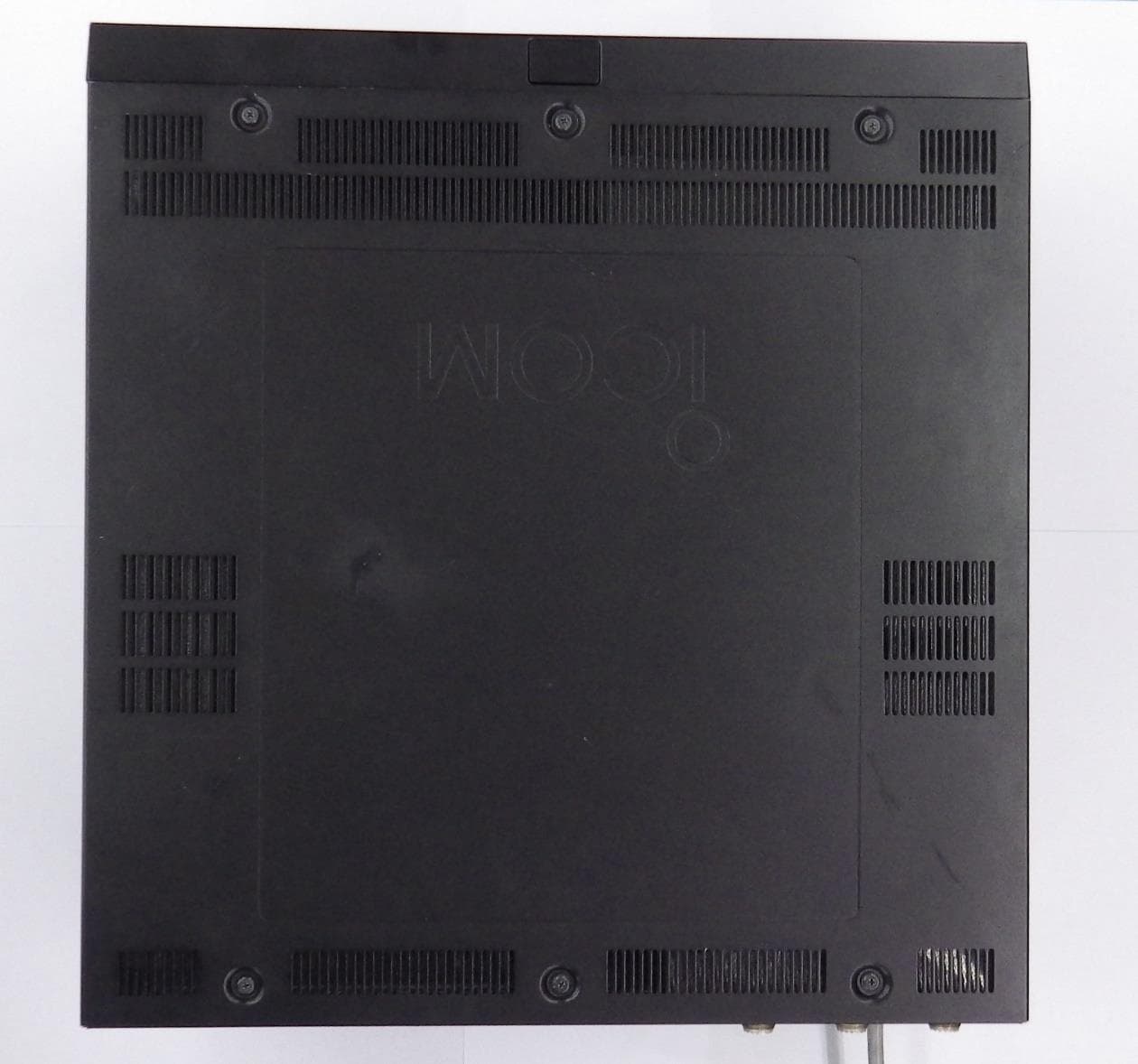
AFJ410900
Jul 09, 2024Linear Amplifier
Equipment Class
AMP - Amplifier