AFJIC-R75
ICOM Incorporated
Click to zoom
Application Details
- Equipment Class
- CSR - Scanning Receiver
- Date of Grant
- Apr 08, 1999
- Application Purpose
- Original Equipment
- Date of Application
- Mar 09, 1999
- Frequency Range
- 30.00000000 - 60.00000000
- Company
- ICOM Incorporated
- Country
- Japan
Documents & Files
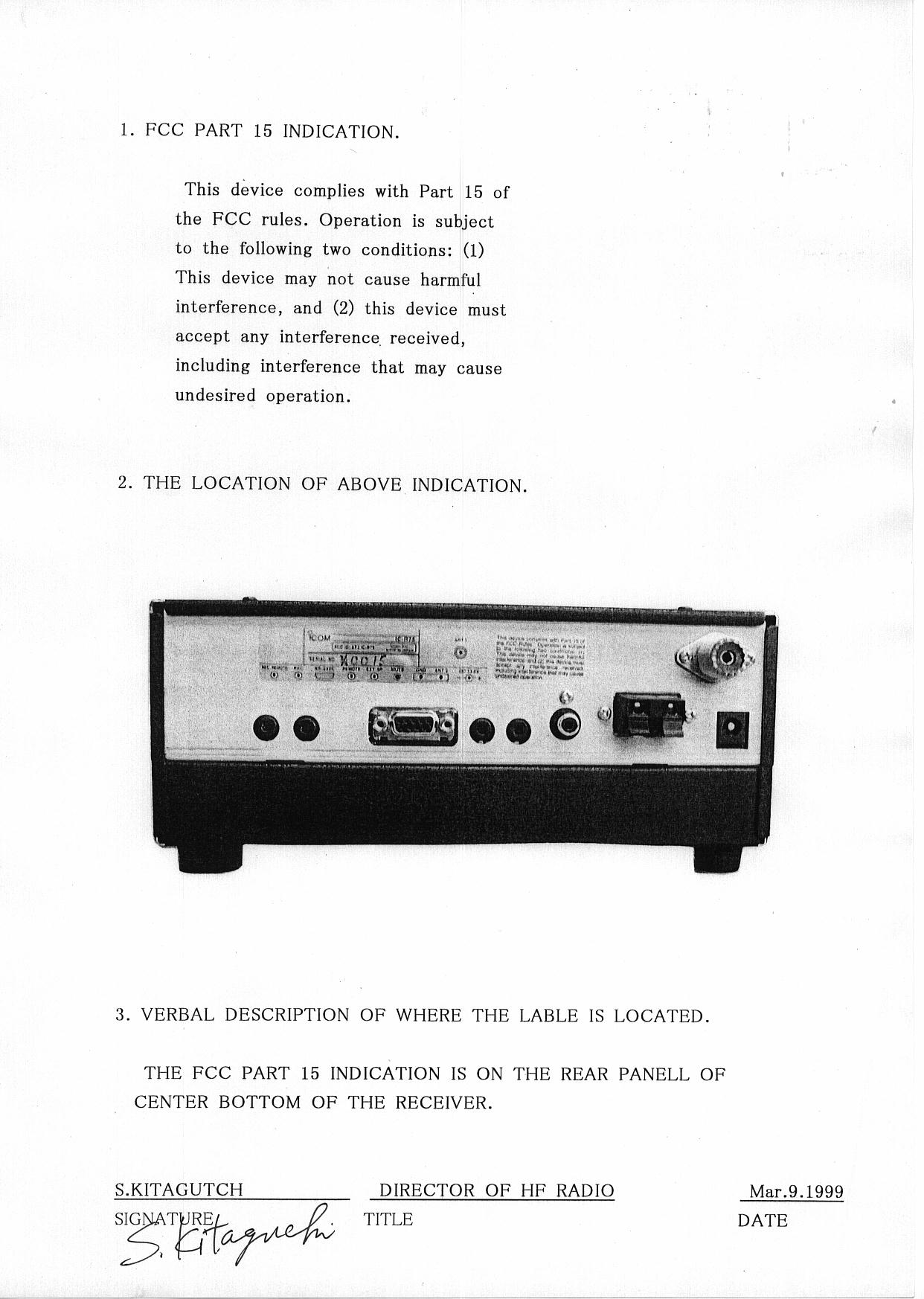
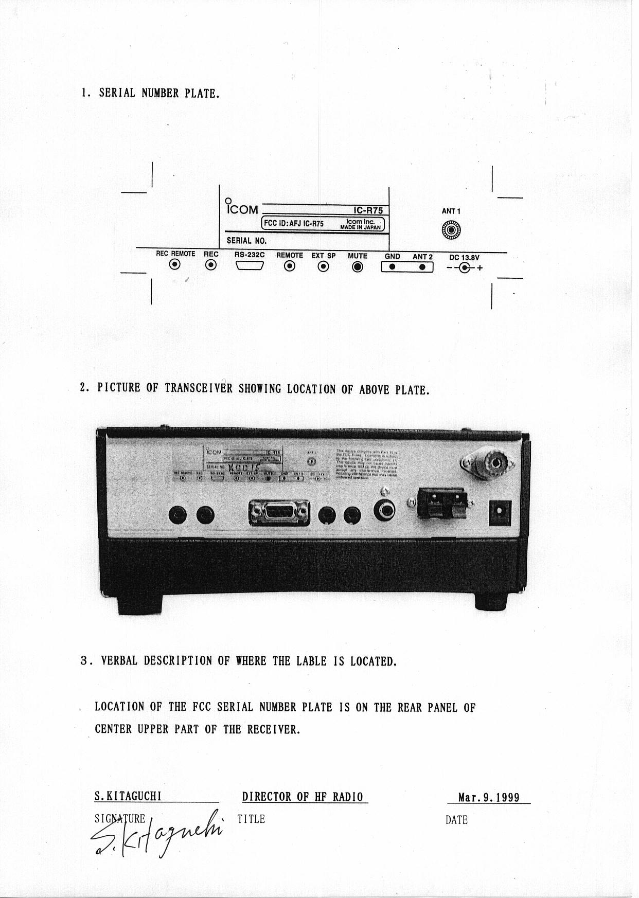
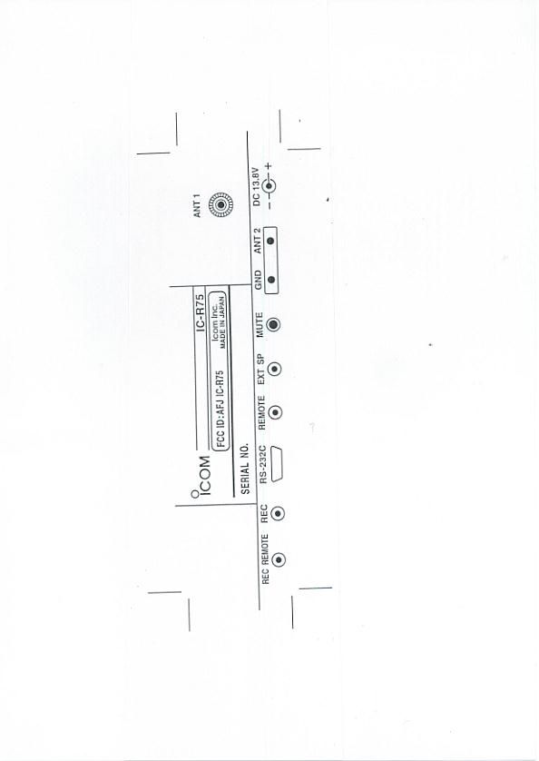
Document Text
Text extracted from the exhibit documents filed with the FCC. Open a document above to read the original.
Users Manual
INSTRUCTION MANUAL COMMUNICATIONS RECEIVER iR75 i IMPORTANT READ THIS INSTRUCTION MANUAL CAREFULLYbefore attempting to operate the re- ceiver. SAVE THIS INSTRUCTION MANUAL.This manual contains important safety and operating in- structions for the IC-R75. EXPLICIT DEFINITIONS RNEVERapply AC to the [DC13.8V] jack on the re- ceiver rear panel. This could cause a fire or ruin the re- ceiver. RNEVERapply more than 16 V DC, such as a 24 V battery, to the [DC13.8V] jack on the receiver rear panel. This could cause a fire or ruin the receiver. RNEVERlet metal, wire or other objects touch any internal part or connectors on the rear panel of the re- ceiver. This may result in an electric shock. NEVERexpose the receiver to rain, snow or any liq- uids. AVOIDusing or placing the receiver in areas with tem- peratures below –10°C (+14°F) or above +60°C (+140°F). Be aware that temperatures on a vehicle’s dashboard can exceed 80°C (+176°F), resulting in per- manent damage to the receiver if left there for ex- tended periods. AVOIDplacing the receiver in excessively dusty envi- ronments or in direct sunlight. AVOIDplacing the receiver against walls or putting anything on top of the receiver. This will obstruct heat dissipation. Place unit in a secure place to avoid inadvertent use by chil- dren. During mobile operation, DO NOToperate the receiver without running the vehicle’s engine. When receiver power is ON and your vehicle’s engine is OFF, the ve- hicle’s battery will soon become exhausted. Make sure the receiver power is OFF before starting the vehicle. This will avoid possible damage to the re- ceiver by ignition voltage spikes. The receiver comes with the following accessories. Qty. qAC adapter (AD-55/A/V)* ..................................... 1 wDC power cable (OPC-869)* ............................... 1 eFuse (FGB 3 A; internal use) ............................... 1 rFuse (FGB 3 A; for DC cable)* ............................ 2 * Either AC adapter + 1 fuse (q, e) or DC power cable + 3 fuses (w, e, r) are supplied depending on versions. PRECAUTIONS SUPPLIED ACCESSORIES Versions of the IC-R75 which display the “CE” symbol on the serial number seal comply with the European har- monised standard ETS300 684 (EMC product standard for Commercially Available Amateur Radio Equipment). WORD R WARNING CAUTION NOTE DEFINITION Personal injury, fire hazard or electric shock may occur. If disregarded, inconvenience only. No risk of personal injury, fire or electric shock. Equipment damage may occur. q w er 1 1 TABLE OF CONTENTS IMPORTANT .............................................................. i EXPLICIT DEFINITIONS ........................................... i PRECAUTIONS ......................................................... i SUPPLIED ACCESSORIES ...................................... i 1 TABLE OF CONTENTS ....................................... 1 2 PANEL DESCRIPTION ................................... 2 – 6 nFront panel ........................................................ 2 nFunction display ................................................. 5 nRear panel ......................................................... 6 3 INSTALLATION AND CONNECTIONS ......... 7 – 10 nGrounding .......................................................... 7 nReceiver stand ................................................... 7 nOptional bracket and carrying handle ................ 7 nConnections ...................................................... 8 nAntenna connection ........................................... 9 nTape recorder connections ................................ 9 nTransceive function ............................................ 9 nFSK and AFSK (SSTV) connections ............... 10 nConnecting to a PC ......................................... 10 4 FREQUENCY SETTING .............................. 11 – 13 nRead me first ................................................... 11 nUsing the keypad ............................................. 11 nFrequency setting ............................................ 12 nDial lock function ............................................. 13 5 RECEIVE FUNCTIONS ............................... 14 – 20 nMode selection ................................................ 14 nSquelch and RF gain ....................................... 14 nTwin PBT operation ......................................... 15 nNoise blanker ................................................... 15 nPreamp ............................................................ 16 nAttenuator ........................................................ 16 nAGC time constant .......................................... 16 nAntenna selection ............................................ 16 nCW reverse mode ............................................ 17 nCW pitch control .............................................. 17 nRTTY reverse mode ........................................ 17 nFilter selection ................................................. 18 nFilter set mode ................................................. 19 nOptional noise reduction function .................... 20 nOptional auto notch function ............................ 20 6 MEMORY OPERATION ............................... 21 – 24 nMemory channels ............................................ 21 nMemory channel selection ............................... 21 nMemory channel programming ........................ 22 nFrequency transferring .................................... 23 nMemory names ................................................ 24 nMemory clearing .............................................. 24 7 SCANS ........................................................ 25 – 27 nScan types ....................................................... 25 nPreparation ...................................................... 25 nProgrammed scan operation ........................... 26 nMemory/select memory scan operation .......... 26 nSetting select memory channels ....................…
Text truncated - open the document above for the full version.
Operational Description
IC-R75 CIRCUIT DESCRIPTION 3 - 1 3-1 RECEIVER CIRCUITS 3-1-1 RF SWITCHING CIRCUIT (MAIN UNIT) The IC-R75 has two antenna connectors. RF signals enter either the [50 ΩANT.] or [450 ΩANT.] connector. RF signals from the [50 ΩANT.] connector are applied to the antenna switching circuit (RL121), and then pass through the low-pass filter (L131, L132, C131–C136). RF signals from the [450 ΩANT.] connector are passed through the L101 to exchange the impeadance value, and are then applied to the antenna switching circuit (RL121). The signals are applied to the low-pass filter (L131, L132, C131–C136). Each RF signals from the [50 ΩANT.] connector or [450 Ω ANT.] connector are chosen by the antenna switching circuit (RL121). 3-1-2 RF FILTER CIRCUIT (MAIN UNIT) The filtered signals are applied to the RX attenuator switch- ing circuit (RL141). Either the signals bypass or pass through the attenuator circuit. The signals are attenuated at 20 dB when passing through the attenuators. The attenuator sys- tem excludes non-linear components between an antenna connector and an attenuator to prevent strong signals from causing distortion. The signals are then applied to the RF fil- ters. The MAIN UNIT has 8 RF bandpass fileters for signals above 2.0 MHz and 2 low-pass filters for signals below 2.0 MHz. (1) Below 1.6 MHz The signals are applied to the low-pass filter consisting of C170–C175, L171–L173 via the limitter circuit (D141, D142). A diode is removed at the entrance of the low-pass filter. This device prevents the diode from causing distortion when receiving very strong signals. A switching diode (D172) is turned on when the “B0” line is “HIGH”. (2) Above 1.6 MHz The signals are applied to the high-pass filter consisting of C161–C163, L161–L164. This filter suppresses strong sig- nals below 1.6 MHz such as broadcasting stations. The filtered signal between 1.6 MHz and 2.0 MHz are applied to the low-pass filter (C182–C187, L182, L183) via the switching diode (D181). The switching diodes (D181, D182) are turned ON when the “B1” line is “HIGH”. The filtered signals above 2.0 MHz are applied to one of 8 bandpass filters depending on the receive frequencies. After passing through a bandpass or low-pass filter, the sig- nals are applied to the pre-amplifier circuit (Q381, Q382, IC391). (3) FILTER SWITCHING CIRCUIT The RF bandpass filter corresponds to the BPF switching voltage (B0–B9) based on the CPU via the shifit registor (IC551, IC552) and driver (IC561, IC562). The switching volt- age of the BPF exit ot improve multi-signal and strong signal characteristics. 3-1-3 PRE-AMPLIFIER CIRCUIT (MAIN UNIT) The pre-amplifier circuit uses low noise junction FETs (Q381, Q382) or wideband amplifier (IC391) to provide gain over a wide frequency range. When the [P.AMP] switch is turned “PREAMP 1”, the signals from the RF filter are amplified by the junction FETs pre- amplifier circuit (Q381, Q382). When the [P.AMP] switch is turned “PREAMP 2”, the signals from the RF filter are amplified by the wideband pre-amplifi- er circuit (IC391). When the [P.AMP] switch is turned “PREAMP OFF”, the sig- nals from the RF filter bypass the pre-amplifiers through D371 and D372. The amplified or bypassed signals are applied to the 1st mixer circuit (Q441, Q442) via the low-pass filter (L431, L432 and C431–CC436). The low-pass filter attenuates at 50 MHz to suppress image frequency. 3-1-4 1ST MIXER AND IF CIRCUITS (MAIN UNIT) The filtered signals are mixed with a 69.0415–129.0115 MHz 1st LO signal to produce a 69.01 MHz 1st IF signal at the 1st mixer circuit (Q441, Q442). The 1st mixer circuit employs a balanced mixer using low- noise junction FETs (Q441, Q442) to expand the dynamic range. The 69.0415–129.0115 MHz 1st LO signal is applied to an LO amplifier (Q411) from the PLL unit via J411, and then passes through the low-pass filter (L421, L422, C422–C425). The filtered signal is applied to the 1st mixer circuit. The 1st IF signal is applied to the crystal bandpass filter(FI- 461) to suppress out-of-band signals. The filtered signal is amplified at a 1st IF amplifier (Q471), and then applied to a 2nd mixer circuit (D491) 3-1-5 2ND MIXER AND IF CIRCUITS (MAIN UNIT) The 1st IF signal is mixed with a 60.0 MHz 2nd LO signal to produce 9 MHz 2nd IF signal at the 2nd mixer (D491, C492, L491, L492). The 6.0 MHz 2nd LO signal is applied to the 2nd mixer from the PLL unit via J491. The 9 MHz 2nd IF signal is applied to the crystal bandpass filter (FI701) to suppress unwanted signals. 3 - 2 The filtered signal enters the noise blanker gate (D711–D714). The signal is applied to L712 to obtain clear reception and is then amplified at the 2nd IF amplifier (Q721). The signal passes through a loose resonator circuit (C726, L721) and then is applied to one of the two crystal bandpass filters. When the [FIL] switch is turned “2F3K”, the filter is selected FI761 which covering the 2.4 kHz bandwith. When the [FIL] switch is turned “2FOP”, the filter is selected an optional filter. When the [FIL] switch is turned “2FTH”, the signal from the 2nd IF amplifier bypass the crystal bandpass filters through D771 and D773. The filtered or bypassed signal is amplified at the buffer amplifier (Q801) and applied to the 3rd mixer circuit (IC811). 3-1-6 NOISE BLANKER CIRCUITS (MAIN UNIT) The IC-R75 uses a trigger noise blanker circuit which removes pulse-type noise signals at the noise blanker gate (D711–D714). The 2nd IF signal passes through the crystal bandpass filter (FI701) to suppress unwanted signals. A portion of the output signal is applied to a noise amplifier circuit (IC731, Q731, Q733) and detected at a noise detector circuit (D731). The detected voltage is applied to a noise blanker gate control cir- cuit (Q735–Q737, D732). The threshold level of the noise blanker gate control circuit (Q735–Q737, D732) is set at 1.0 V on SSB mode (In case of AM mode, is set at 1.6 V). When the detected voltage exceeds the threshold level, Q737 outputs a blanking signa…
Text truncated - open the document above for the full version.
Parts List/Tune Up Info
SECTION 4 ADJUSTMENT PROCEDURES 4-1 PREPARATION ‘ REQUIRED TEST EQUIPMENT ‘ CONNECTION EQUIPMENT DC power supply Frequency counter Audio generator DC Voltmeter GRADE AND RANGE Output voltage: 13.8 V DC Current capacity: 2 A or more Frequency range: 0.1–60 MHz Frequency accuracy : ±1 ppm or better Sensitivity: 100 mV or better Frequency range: 0.1–60 Hz Measuring range: 0.01–10 mV Input impedance: 50 kΩ/V DC or better EQUIPMENT Oscilloscope AC millivoltmeter External speaker Standard signal generator (SSG) GRADE AND RANGE Frequency range: DC–20 MHz Measuring range: 0.01–20 V Measuring range: 10 mV–10 V Input impedance: 8 Ω Capacity: 4 W or more Frequency range: 0.1–300 MHz Output level: 0.1 μV–32 mV (–127 to –17 dBm) 50 Ω ANT 450 Ω ANT DC IN EXT SP REMOTE connector Standard Signal Generator NOTE: The [450 Ω] ANT jack is not used for adjustment Speaker AC milli-voltmeter DC power supply 13.8 V / 10A 1/8" (3.5 mm) 2-conductor plug Shorten inner and outer plugs Terminator for the entering adjustment mode 4-2 PLL ADJUSTMENT REFERENCE FREQUENCY VCO VOLTAGE 1ST LO VOLTAGE 3RD LO VOLTAGE 3RD LO FREQUENCY BFO VOLTAGE ADJUSTMENT ADJUSTMENTADJUSTMENT CONDITION MEASUREMENT VALUE POINT UNITLOCATIONUNITADJUST 1 2 1 2 3 4 1 1 1 1 2 • Displayed frequency : 29.99999 MHz • Mode: USB • Displayed frequency : 29.99999 MHz • Mode: USB • Displayed frequency : 0.03000 MHz • Mode: USB • Displayed frequency : 60.00000 MHz • Mode: USB • Displayed frequency : 30.00000 MHz • Mode: USB • Displayed frequency : 30–60.00000 MHz • Mode: USB • Displayed frequency : 30–60.00000 MHz • Mode: USB • Displayed frequency : 9.4615 MHz • Mode: FM • Displayed frequency : 14.100000 MHz • Mode: USB • Displayed frequency : 14.100000 MHz • Mode: AM PLL PLL PLL PLL PLL PLL Connect the fre- quency counter to P1. Connect the RF voltmater to P1. Connect the DC voltmeter to HCP71. Connect the RF voltmeter to P91. Connect the RF voltmeter to P91. Connect the fre- quency counter to P151. Connect the RF voltmeter to P201. 60.00000 MHz Maximum voltage 4.0 V More than 0.8 V 4.0 V More than 0.8 V More than 0.18 V More than 0.022 V 9.4614–9.4616 MHz More than 0.022 V Less than 280 μV PLL PLL PLL L2 L4, L5 C86 Verify C76 Verify Verify Verify Verify Verity *This output level of the standard signal generator (SSG) is indicated as SSG’s open circuit. P201 BFO voltage check point P151 3rd LO frequency check point P1 Reference frequency check point P91 1st and 3rd LO voltage check point C76 VCO voltage adjustment L2 Reference frequency adjustment (for output frequency is 60.0000 MHz) HCP71 VCO voltage check point C86 L5 Reference frequency adjustment (for output voltage is maximum) L4 • PLL UNIT 4-3 RECEIVER ADJUSTMENTS RECEIVER SENSITIVITY 1ST MIXER BALANCE ADJUSTMENT ADJUSTMENTADJUSTMENT CONDITION MEASUREMENT VALUE POINT UNITLOCATIONUNITADJUST 1 2 1 • Displayed frequency : 14.10000 MHz • Mode : USB • PREAMP1: ON • ANT select: ANT1 • AGC: FAST • NOISE BLANKER: OFF • RF/SQL: CENTER • PBT1/PBT2: CENTER • IF FILTER1: 2.4 kHz • IF FILTER2: 2.4 kHz • Connect an SSG to the antenna connector1 and set as: Frequency: 14.10150 MHz Level: 22 μV* (–13 dBμ) Modulation: OFF • Receiving • Displayed frequency : 0.10000 MHz • PREAMP1: OFF • set an SSG level as : OFF • Receiving Rear Panel Rear panel Connect the AC milli-volt meter to the [EXT SP] jack with an 8 Ωload. Connect an oscillo- scope to the [EXT SP] jack with 8 Ω load. Pre-set to center Maximum output level Minimum noise level MAIN MAIN MAIN R444 R898 L443, L461, L462, L471, L701, L711, L712, L891, L892, L911 L443, R444 *This output level of the standard signal generator (SSG) is indicated as SSG’s open circuit. Receiver sensitivity adjustment Pre-set to center before receiver sensitivity adjustment 1st mixer balance adjustment EXT SP JACK Receiver sensitivity and 1st mixer balance check point • MAIN UNIT R893 R444 L701 L711 L712 L471 L462 L461 L443 L891 L892 L911 R444 L443 RECEIVER ADJUSTMENTS (continued) 1ST IF FILTER RECEIVER TOTAL GAIN ADJUSTMENT ADJUSTMENTADJUSTMENT CONDITION MEASUREMENT VALUE POINT UNITLOCATIONUNITADJUST 1 1 2 • Displayed frequency : 14.10000 MHz • Mode: FM • PREAMP1: ON • IF FILTER1: 15 kHz • IF FILTER2: 6 kHz • set an SSG as Frequency: 14.10000 MHz Level: 0.32 μV* (–10 dBμ) Deviation: ±3.5 kHz Modulation: 1 kHz • Receiving • Displayed frequency : 14.10000 MHz • Mode: USB • PREAMP1: OFF • IF FILTER1: 2.4 kHz • IF FILTER2: 2.4 kHz • Set an SSG as Frequency: 14.10150 MHz Level: 500 μV* (54 dBμ) Modulation: OFF • Set an SSG level as : OFF • Receiving Rear panel Rear panel Connect the AC milli-volt meter to the [EXT SP] jack with an 8 Ωload. Connect the AC milli-volt meter to the [EXT SP] jack with an 8 Ωload. Maximum output level 0 dB (1.0 V) –30 dB (10 mV) MAIN Front panel MAIN L461, L462 [AF GAIN] control R898 *This output level of the standard signal generator (SSG) is indicated as SSG’s open circuit. EXT SP JACK 1st IF filter and receiver total gain check point R898 Receiver total gain adjustment 1st IF filter adjustment • MAIN UNIT L462 L461 EXT SP JACK Noise blanker check point after apply the noise signal Noise blanker adjustment before apply the noise signal R736 • MAIN UNIT CP731 Noise blanker check point before apply the noise signal • Noise blanker adjustment after apply the noise signal • Pre-set to center before apply the noise signal L731 L732 RECEIVER ADJUSTMENTS (CONTINUED) NOISE BLANKER ADJUSTMENT ADJUSTMENTADJUSTMENT CONDITION MEASUREMENT VALUE POINT UNITLOCATIONUNITADJUST 1 2 • Displayed frequency : 14.10000 MHz • Mode: USB • Noise Blanker: OFF • PREAMP1.: ON • Set an SSG as Frequency: 14.10000 MHz Level: 18 μV* (25 dBμ) Modulation: OFF • Apply the following signal to the [ANT1] connector MAIN Rear Panel Connect the oscillo- scope to the check point CP731. Connect the oscillo- scope to the [EXT SP] jack with an 8 Ω load. Pre-set to center Minimun voltage Noise is blanked when the [NB] switch is ON. MAIN MAIN R736 L731, L732 R736 *This output level of the standard signal…
Text truncated - open the document above for the full version.
Parts List/Tune Up Info
IC-R75 CIRCUIT DESCRIPTION 3 - 1 3-1 RECEIVER CIRCUITS 3-1-1 RF SWITCHING CIRCUIT (MAIN UNIT) The IC-R75 has two antenna connectors. RF signals enter either the [50 ΩANT.] or [450 ΩANT.] connector. RF signals from the [50 ΩANT.] connector are applied to the antenna switching circuit (RL121), and then pass through the low-pass filter (L131, L132, C131–C136). RF signals from the [450 ΩANT.] connector are passed through the L101 to exchange the impeadance value, and are then applied to the antenna switching circuit (RL121). The signals are applied to the low-pass filter (L131, L132, C131–C136). Each RF signals from the [50 ΩANT.] connector or [450 Ω ANT.] connector are chosen by the antenna switching circuit (RL121). 3-1-2 RF FILTER CIRCUIT (MAIN UNIT) The filtered signals are applied to the RX attenuator switch- ing circuit (RL141). Either the signals bypass or pass through the attenuator circuit. The signals are attenuated at 20 dB when passing through the attenuators. The attenuator sys- tem excludes non-linear components between an antenna connector and an attenuator to prevent strong signals from causing distortion. The signals are then applied to the RF fil- ters. The MAIN UNIT has 8 RF bandpass fileters for signals above 2.0 MHz and 2 low-pass filters for signals below 2.0 MHz. (1) Below 1.6 MHz The signals are applied to the low-pass filter consisting of C170–C175, L171–L173 via the limitter circuit (D141, D142). A diode is removed at the entrance of the low-pass filter. This device prevents the diode from causing distortion when receiving very strong signals. A switching diode (D172) is turned on when the “B0” line is “HIGH”. (2) Above 1.6 MHz The signals are applied to the high-pass filter consisting of C161–C163, L161–L164. This filter suppresses strong sig- nals below 1.6 MHz such as broadcasting stations. The filtered signal between 1.6 MHz and 2.0 MHz are applied to the low-pass filter (C182–C187, L182, L183) via the switching diode (D181). The switching diodes (D181, D182) are turned ON when the “B1” line is “HIGH”. The filtered signals above 2.0 MHz are applied to one of 8 bandpass filters depending on the receive frequencies. After passing through a bandpass or low-pass filter, the sig- nals are applied to the pre-amplifier circuit (Q381, Q382, IC391). (3) FILTER SWITCHING CIRCUIT The RF bandpass filter corresponds to the BPF switching voltage (B0–B9) based on the CPU via the shifit registor (IC551, IC552) and driver (IC561, IC562). The switching volt- age of the BPF exit ot improve multi-signal and strong signal characteristics. 3-1-3 PRE-AMPLIFIER CIRCUIT (MAIN UNIT) The pre-amplifier circuit uses low noise junction FETs (Q381, Q382) or wideband amplifier (IC391) to provide gain over a wide frequency range. When the [P.AMP] switch is turned “PREAMP 1”, the signals from the RF filter are amplified by the junction FETs pre- amplifier circuit (Q381, Q382). When the [P.AMP] switch is turned “PREAMP 2”, the signals from the RF filter are amplified by the wideband pre-amplifi- er circuit (IC391). When the [P.AMP] switch is turned “PREAMP OFF”, the sig- nals from the RF filter bypass the pre-amplifiers through D371 and D372. The amplified or bypassed signals are applied to the 1st mixer circuit (Q441, Q442) via the low-pass filter (L431, L432 and C431–CC436). The low-pass filter attenuates at 50 MHz to suppress image frequency. 3-1-4 1ST MIXER AND IF CIRCUITS (MAIN UNIT) The filtered signals are mixed with a 69.0415–129.0115 MHz 1st LO signal to produce a 69.01 MHz 1st IF signal at the 1st mixer circuit (Q441, Q442). The 1st mixer circuit employs a balanced mixer using low- noise junction FETs (Q441, Q442) to expand the dynamic range. The 69.0415–129.0115 MHz 1st LO signal is applied to an LO amplifier (Q411) from the PLL unit via J411, and then passes through the low-pass filter (L421, L422, C422–C425). The filtered signal is applied to the 1st mixer circuit. The 1st IF signal is applied to the crystal bandpass filter(FI- 461) to suppress out-of-band signals. The filtered signal is amplified at a 1st IF amplifier (Q471), and then applied to a 2nd mixer circuit (D491) 3-1-5 2ND MIXER AND IF CIRCUITS (MAIN UNIT) The 1st IF signal is mixed with a 60.0 MHz 2nd LO signal to produce 9 MHz 2nd IF signal at the 2nd mixer (D491, C492, L491, L492). The 6.0 MHz 2nd LO signal is applied to the 2nd mixer from the PLL unit via J491. The 9 MHz 2nd IF signal is applied to the crystal bandpass filter (FI701) to suppress unwanted signals. 3 - 2 The filtered signal enters the noise blanker gate (D711–D714). The signal is applied to L712 to obtain clear reception and is then amplified at the 2nd IF amplifier (Q721). The signal passes through a loose resonator circuit (C726, L721) and then is applied to one of the two crystal bandpass filters. When the [FIL] switch is turned “2F3K”, the filter is selected FI761 which covering the 2.4 kHz bandwith. When the [FIL] switch is turned “2FOP”, the filter is selected an optional filter. When the [FIL] switch is turned “2FTH”, the signal from the 2nd IF amplifier bypass the crystal bandpass filters through D771 and D773. The filtered or bypassed signal is amplified at the buffer amplifier (Q801) and applied to the 3rd mixer circuit (IC811). 3-1-6 NOISE BLANKER CIRCUITS (MAIN UNIT) The IC-R75 uses a trigger noise blanker circuit which removes pulse-type noise signals at the noise blanker gate (D711–D714). The 2nd IF signal passes through the crystal bandpass filter (FI701) to suppress unwanted signals. A portion of the output signal is applied to a noise amplifier circuit (IC731, Q731, Q733) and detected at a noise detector circuit (D731). The detected voltage is applied to a noise blanker gate control cir- cuit (Q735–Q737, D732). The threshold level of the noise blanker gate control circuit (Q735–Q737, D732) is set at 1.0 V on SSB mode (In case of AM mode, is set at 1.6 V). When the detected voltage exceeds the threshold level, Q737 outputs a blanking signa…
Text truncated - open the document above for the full version.
Test Report
HGL IMAGES TO PDF TEST RUN TO: BRYAN: FROM: RICHARD MUNDY VAR VCC LED TRANSMIT:RED CHANNEL BUSY:GREEN BACK_LIGHT LCD AlphaNumeric Type:112(8*14)+6(ICON)Numeric Type :35(5*7)+6(ICON) LCDCONTROLLER ROM8K BYTES CPU RAM256 BYTES 8-BITS I/O PORT A/D PSCKPSDTPSRQRESET- DRIVERRECEIVER RESET PSCKPSDTPSRQPWSW-PTT-SW_CA+HOOK_SWINT_MIC_H 1234567891011121314 J404 To_RADIO GNDSP_LINT_SP_HGND3HS_RXINT_MIC_L CLKSF 3.6864MHz KEY_SW MONITOR+-SCANMENU 123456789 101112 J402 CH3GNDCH1CH2 VCC PWSW-CH0VOL_HVOL_WVOL_LGND MIC_LOMIC_HIPTT-GNDSW_CA+ 123456789 J401To_MIC EXCKMDIN- HOOK_SWRX_AUDIO 12 J403To_Speaker INT_SP_HSP_L MA00-TC-0084/TC-0085LCD Board Unit(Numeric Type / Alpha Numeric Type) PRG_RXD (CPU) CMP AK2344 AMP6 EXT_MOD MUTEMIC (CPU) INT_MIC_HEXT_MIC_HINT_MIC_MMIC_MUTE MICHFMIC AMP1 VR1 SW1 AGC HPF fc:300Hz SW3 VR9MUX PE LIMITER PEO LIMIN SW4 VR10 LPF fc:3KHz60log SW5 ADD1 EXTIN1 SW7 SW6 SW8 VR4 VR5 SMF1 SW9 TX_MOD RX_AUDIO STD- (CPU) VR6 SMF3 DTMFReceiver V6EN SW12 VR3 CTCSS SW3 CTCSSGEN SW11 SW3 ADD2 M-TONELPF2M-TONELPF1 M2ENM1EN VR11 M-TONEGEN1M-TONEGEN2 Multi-tone & DTMF (CPU) DCS_TX AMP3 BPF1 CTCSS LIMITER CMP1AMP7 CTCSSBPF2 CTCSS DETECTOR (CPU)(CPU) PHSDET CTCDT (CPU)(CPU) TONEDET SDI BPFCONT M-TONE DET DA1 M-TONE BPFDA2 CONTROL LOGIC DE SW10 AMP2 VR2 (CPU)(CPU)(CPU) RX_AFRESET-SDTSCKCSASPAPCLK (CPU) GE_TXD GE-STAR(TX_AUD) GE-STAR GE-STAR(RX_AUD) VCC (CPU)(CPU)(CPU) GE_MTEGE_RXDGE_MCKHS_RX_A INT_SP_H SP_H SP_PA 1 2 3 RX_AUDIO MUTE ATTBUF RX_AF VOL SUM RX_AUDIO (CPU)(CPU)(CPU)(CPU) GE_CCKVOLUDVOLINCVOLCSALERAT_T (CPU)(CPU)(CPU) RXMTRXSTBY MA00-TC-0081Radio Cntorol UnitAUDIO.blk SP_L (3/3) IGN_A+ SW_A+ SW_CA+ 1 2 3 A+IGNITION_A+GND Analog Power PSCK PWSW-+9V SCI0(CK0) SWCONT P52 CPU_DOCPU_DO AVR P27P25 TXENB+ DPTT++5VDNSQ+ APCREFNSQREFNSQFST- CPU_DOCPU_DICPU_DACPU_DA P76P90P77P20 SCI0SCI1 P50P51P70P84P85 CPU_DISCI0(RD0)SCI0(TD0)SCI1(TD1)SCI1(RD1) PRGLOGICDIR CONTROL PRG_RXD PTT-/PRG_TXDPSDT PSRQINT_MIC_MEXT_IN S_DT_OUT S_DT_INHOOK CPU_DICPU_DI L_SEL CPU_DO PTT- CPU_DICPU_DI P83P71P73P41P72 ROM CPU CPU_DOCPU_DICPU_DOCPU_DOCPU_DOCPU_DOCPU_DOCPU_DO P91P23P34P21P26P10P11P13P75 CPU_AD W/N PLLFST- VSFT+ PLLLOCK- VCOENB+PLLENB+ SCK-SDT- TYPE SDO GE_TXDGE_CCK GE_MCKGE_RXDGE_MTE CSASP CPU_DICPU_DOCPU_DOCPU_DICPU_DICPU_DICPU_DO P67P30P12P14P60P61P65 RAM P92P80P82P75 CPU_DO PWFAL CPU_DI RESTAT CPU_DO IGN_S CPU_DI DET PW_FAIL EXT_OUT EEPROM CPU_DOCPU_IO 7.3728MHz P86P97 INPUT CAPTUER1 CPU_DICPU_DOCPU_DICPU_DICPU_DO F_SELF_CLK CPU_DO P62P63P64P44P17P16 filter DCS_TXCTCDTPHSDT TONEDET RUS- MIC_MUTE APCLK RXMT VOLUD VOLINC VOLCS ALEART_T STD- CPU_DOCPU_DOCPU_DO CLOCK/2 CPU_DOCPU_DOCPU_DOCPU_DO P46P96 CLOCK P37P36P35P34P33P32 CPU_DI P66 INPUT CAPTUER2 TIMER P94P95 CLKSFT CPU_DOCPU_DOCLOCKRESET RESETLOGIC LOGIC_OUT 1/2 MA00-TC-0081Radio Control UnitLOGOC.blk RESET- (2/3) A+IGNITION_A+GND 123456 J601From DC Power Supply Unit 123456789101112131415161718192021222324 J602 To TRX Board Unit LOGICLOGIC.blk PSCK GNDPTT-PRG_RXDPSDTPSRQ A+ IGNITION_A+ GND PWSW-IGN_A+SW_CA+HOOK_SW SCKSDTSDI CSASP GE_TXDGE_CCKGE_MCKGE_RXDGE_MTEDCS_TX CTCDTPHSDT MIC_MUTEALERAT_T APCLK RESET- INT_MIC_MRUS-EXT_INEXT_OUTS_DT_INS_DT_OUT RXMTSTD- VOLCS VOLINC VOLUD NSQ+ PLLLOCK+ PLLENB- NSQREF SCK- NSQFST- SDT-TYPE PLLFST- W/N DPTT+VSFT+ GND VCOENB+ +9VS TXENB+ SW_A+ APCREF MTNDT SW_CA+CSCK-CSDT+CSRQ+PWSW-PTT-HOOK_SWINT_MIC_HI 123456789 1011121314 J602To LCD Board Unit INT_MIC_LHS_RX_AGND3INT_SP_HSP_LGND APCREFSW_A+TXENB++9VSVCOENB+GNDVSFT+BPFCONTDPTT+W/NPLLFST-TYPETX_MODGND1GND2RX_AFPLLENB-DSCAFSDT-NSQREFSCK-NSQREFPLLLOCK+NSQ+ AUDIOAUDIO.blk SCK GE_TXDGE_CCKGE_MCKGE_RXDDCS_TXCTCDTPHSDTGE_MTECSASP HS_RX_A RESET-APCLKMIC_MUTE PRG_RXD SP_L INT_MIC_MEXT_MIC_HINT_MIC_LINT_MIC_HALERAT_TSDTSDI SP_H INT_SP_H GND3 EXT_MOD TX_MOD BPFCONT RX_AF RXMTSTD-VOLCSVOLINCVOLUD GND2 MTNDT SP_LGNDEXT_MODSP_HDISCAFSW_CA+HOOK_SWINT_SP_HEXT_MICPTT- 123456789 101112131415161718 J603Option IGN_A+INT_MIC_MS_DT_INS_DT_OUTEXT_INEXT_OUTRUSGND1 MA00-TC-0081Radio Control UnitBlock Diagram (1/3) 1 TE1 A+ 1 TE5TE To RF_POWER_AMP B_A+ To Radio_control 123456 ZC1U-PK-2224A #C111000P C4220u #C50.1u #C101000P #C81000P #CD4D1F20 CD3NV022D05 #C91000P C2220u #C61000P #C71000P #C30.1u CD2MR751 CD1NV022D05 1 TE2 IGNITION_A+ 1 TE3 GND 1 TE4TE NOTE1. # IDENTIFIES CHIP COMPONENTS. MD00-TB-0038DC Power Supply Unit 88 16 #IC51074HC123 #C6930.1u 7 14 74HC14 16 HC4053 #IC604 #IC605 #C6870.1u #C6890.1u VCC TC7W14F 8 4 74HC125 7 14 #IC602 #IC603 #C6860.1u 1/2W #C71933u #C7200.1u IN 1 OUT 3 GND 2 #IC612L78M05T #C721100u #C7220.1u #R75733 J605ADIC-252 1 2 3 J605FFC-3AMEP1 #TR6112SJ280S #R758 10K #TR613RN2302 #TR612RN1304 #C717220u #C7180.1u C 1 C 3 G 2 #FL601NFM41R11C222 123456 #J601DF3-6P-2V(50) #F6015.0A GNDGNDA+A+IGNITION_A+ 1 3 #CD611A MA133 3 2 #CD611B MA133 #R761 100 1 3 #CD612A MA133 3 2 #CD612B MA133 #C723 220P #C724 220P #R762 100 1 3 #CD613A MA133 3 2 #CD613B MA133 #C725 220P #R763 100 1 3 #CD614A MA133 3 2 #CD614B MA133 #R764 100 1/2W #R7591.0K #TR615RN1303 #TR614 2SB1302T #R760560 LOGICLOGIC.sch SW_A+ +5VDPSCK-PSDT+PTT-/PRG_TXD RESET- 3.6864MHz MIC_MUTE RXMT+VOLUDVOLIC ALERAT+ MTNDTPHSDTCTCDT PRG_RXD-S_DT_IN+S_DT_OUT+GNDI_MICM VOLCS HOOK- +9V PSRQ+IGN_S- APCREF VCOENB+ TXENB+ DPTT+VSFT+ PLLENB- NSQREF PLLLOCK+ NSQ+SDT-SCK- VPP+ DCSTX- STD+ W/N TYPE PLLFST-NSQFST- RUS+SCK+SDT+SDO+ CSASP-RSASP- GE_CCK-GE_TXD+GE_RXD+GE_MTE+GE_MCK+ TN_TX EMR/HOME-HORN/SPKR- 7 74HC74 14 #IC610 #C7070.1u #C75822u #C7590.1u C 1 C 3 G 2 #FL602 NFM41R11C222 #C75422u #C7550.1u 123456789101112131415161718192021222324 #J604 20035A-24G2 SW_A+TXENB+APCREF+9VS GNDGND1GND2DPTT+VCOENB+BPFCONTNSQREFW/NNSQFST-SCK-SDT-PLLENB-PLLLOCK+VSFT+PLLFST-RX_AFDSCAFTX_MODTYPE AUDIOAUDIO.sch SW_A+ +5VDRESET-3.6864MHzMIC_MUTERXMT+VOLCSVOLUDVOLICALERAT+MTNDTPHSDTCTCDTI_MICMPRG_RXD-EXT_MODEXT_MIC_HINT_MIC_HGND HS_RX_A SP_LSP_H BPFCONT TX_MOD RX_AF +9V INT_SP_H GND_A GND2GND1GND3 INT_MIC_LDCSTX-STD+SCK+SDT+SDO+CSASP-RSASP-GE_CCK-GE_TXD+GE_RXD+GE_MTE+GE_MCK+TN_TX #C726 220P 1 3 #CD615A MA133 3 2 #CD615B MA133 #C727 220P 1 3 #CD616A MA133 3 …
Text truncated - open the document above for the full version.
Contact Information
Applicant
Atsushi Tomiyama(General Manager)
Technical Contact
Icom America IncMasaaki Takahashi
[email protected](425) 454-8155
2380 116th Ave NE · Bellevue, Washington · United States
Non-Technical Contact
Icom America IncMasaaki Takahashi
[email protected](425) 454-8155
Test Firm
Japan Quality Assurance Org.Katsumi Nishii
Technical Specifications
| # | Rule Parts | Frequency Range | Power Output | Tolerance |
|---|---|---|---|---|
| 1 | 15B | 30 MHz - 60 MHz | - | ppm |
Other Applications from ICOM Incorporated
AFJ453700
Jul 23, 2026Mobile Transceiver
Equipment Class
DTS - Digital Transmission System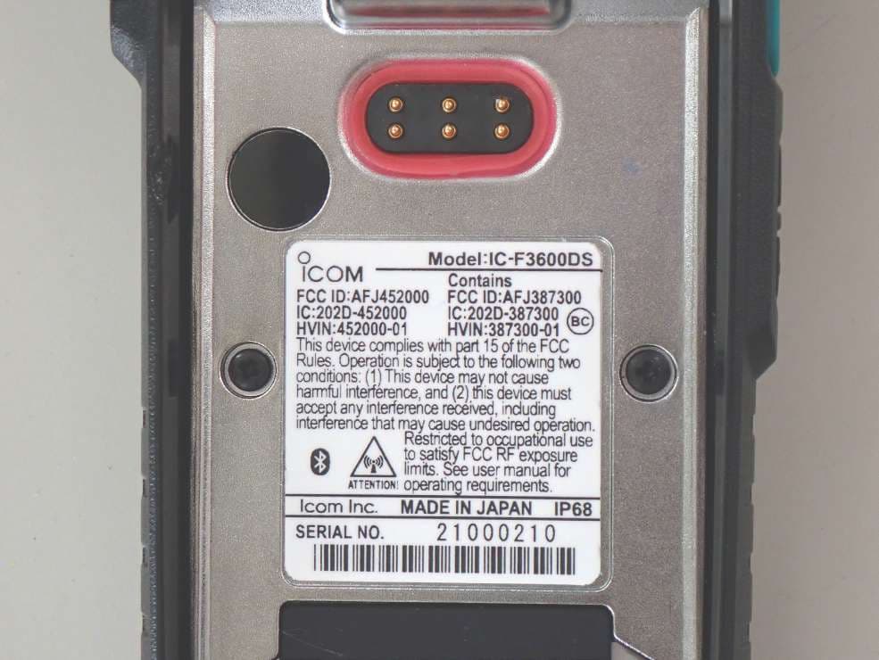
AFJ452000
Jun 02, 2026VHF DIGITAL TRANSCEIVER
Equipment Class
TNF - Licensed Non-Broadcast Transmitter Held to Face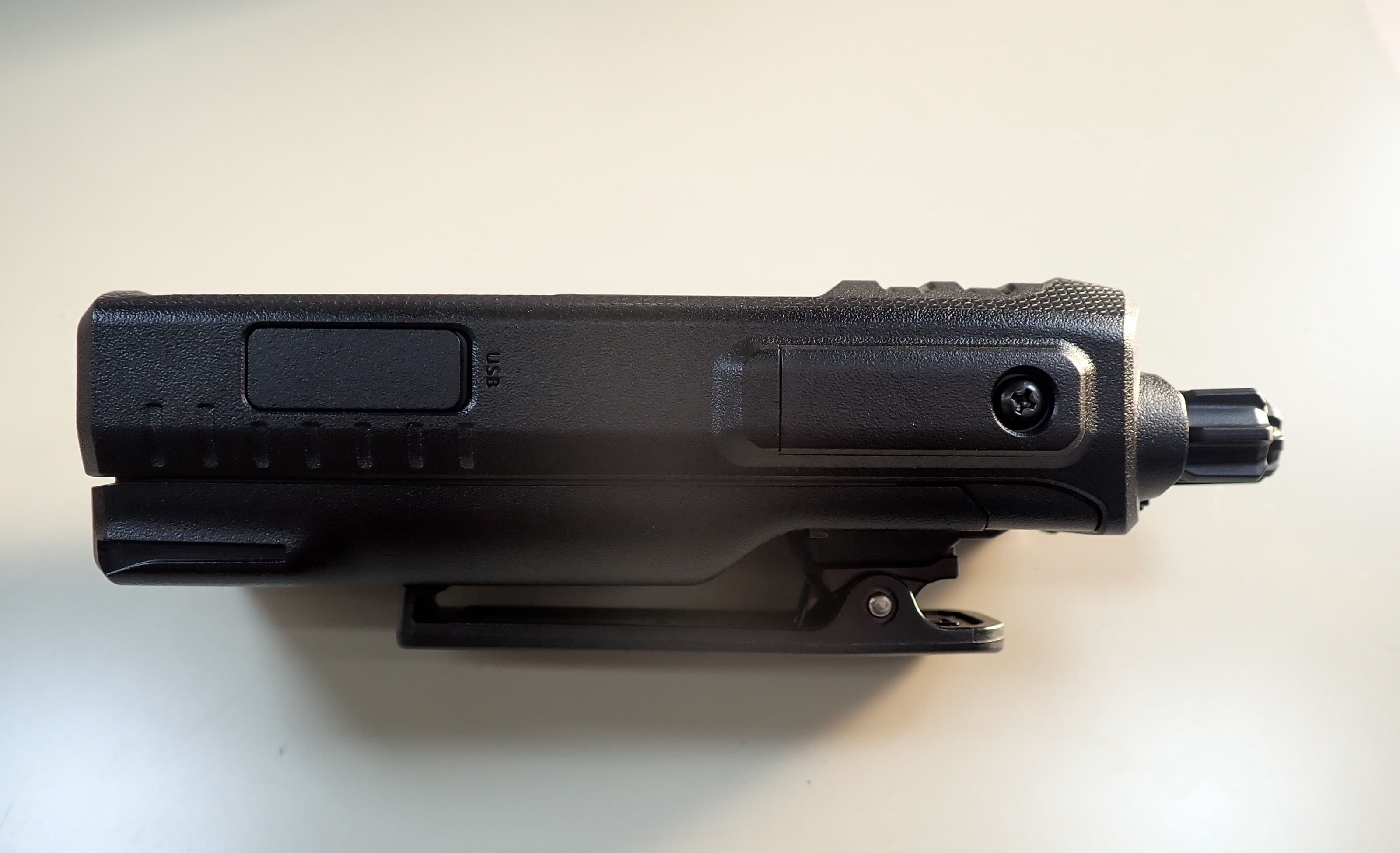
AFJ452100
May 12, 2026UHF DIGITAL TRANSCEIVER
Equipment Class
TNF - Licensed Non-Broadcast Transmitter Held to Face
AFJ444500
Sep 12, 2024Scanning Receiver
Equipment Class
CSR - Scanning Receiver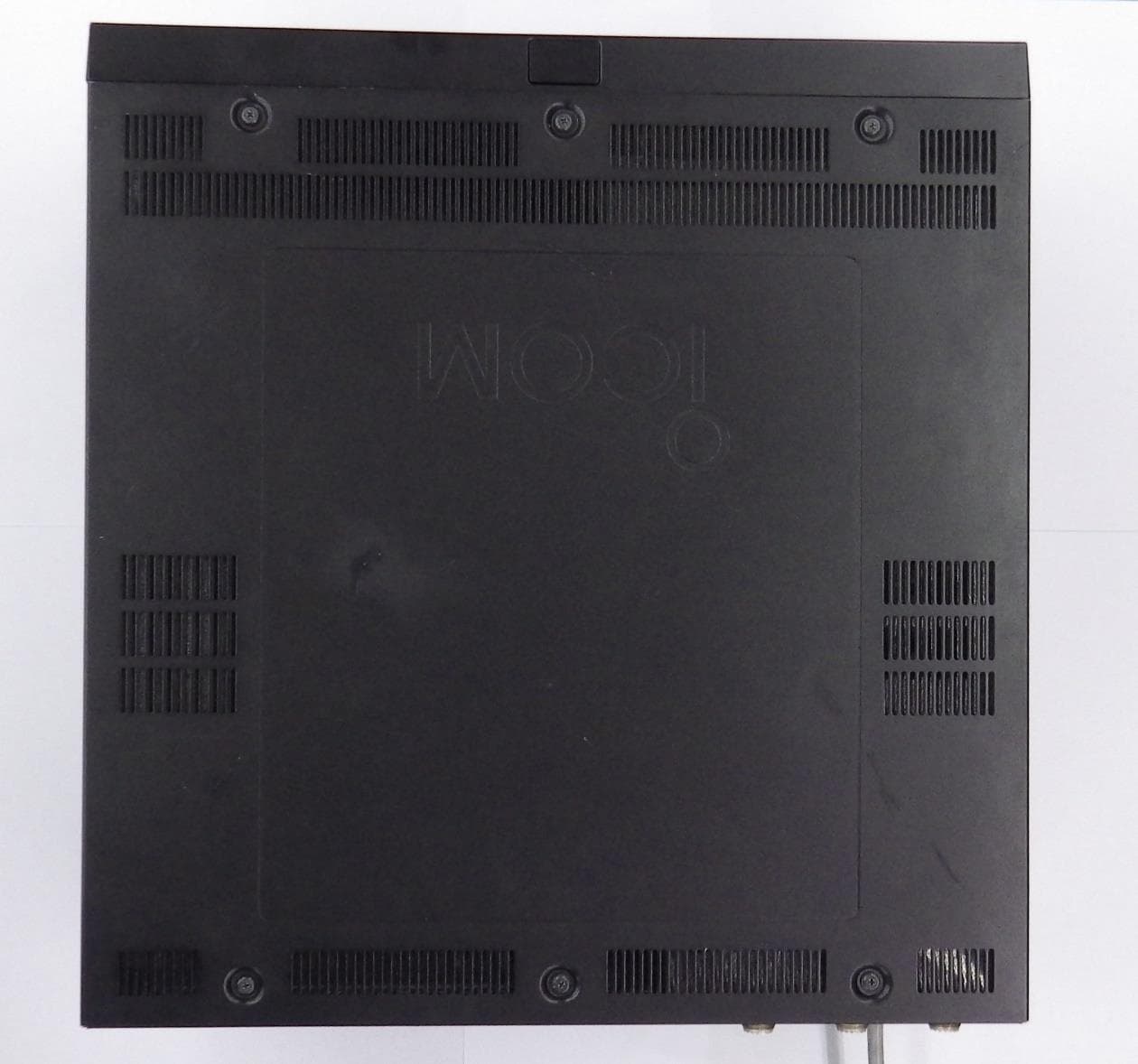
AFJ410900
Jul 09, 2024Linear Amplifier
Equipment Class
AMP - Amplifier