ARURPU499AUHF Land Mobile Radio
RELM Communications Inc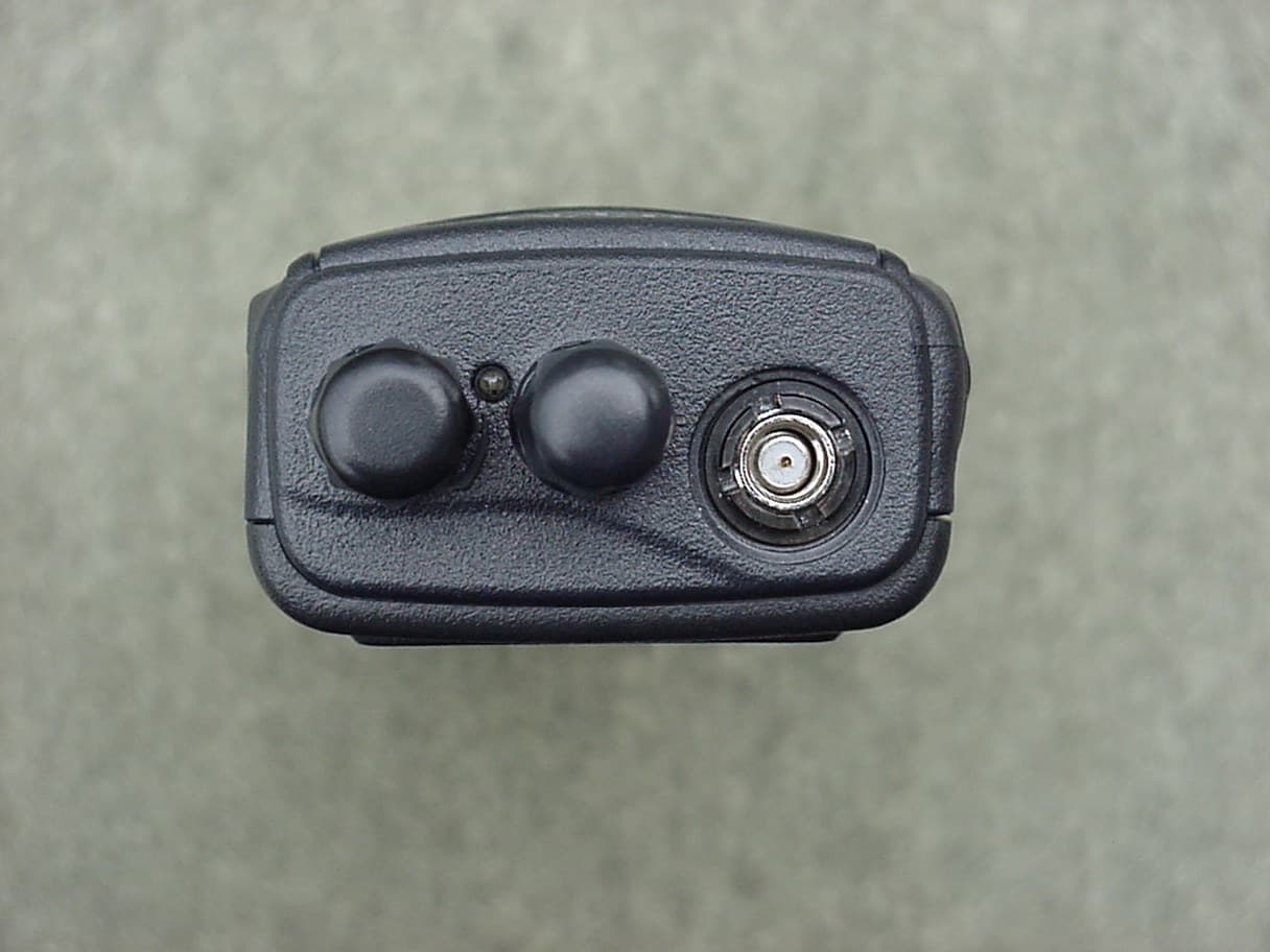
Click to zoom
Application Details
- Equipment Class
- TNF - Licensed Non-Broadcast Transmitter Held to Face
- Date of Grant
- Apr 25, 2004
- Application Purpose
- Original Equipment
- Date of Application
- Apr 25, 2004
- Equipment Note
- UHF Land Mobile Radio
- Frequency Range
- 450.00000000 - 470.00000000
- Company
- RELM Communications Inc
- Country
- United States
Documents & Files
Document Text
Text extracted from the exhibit documents filed with the FCC. Open a document above to read the original.
Users Manual
2 Preface Scope This manual is intended for use by qualified technicians familiar with similar types of communication equipment. It contains all service information and data required for the equipment. Caution The following precautions are recommended for personnel safety: y DO NOT transmit until all RF connectors are verified secure and all connectors are properly terminated. y SHUT OFF the power and DO NOT operate this equipment near electrical blasting caps or in a potential explosive atmosphere. y This equipment should be serviced by qualified technicians only. 3 Brief Introduction (1) ANTENNA (2) CHANNEL SELECTOR KNOB Used to select channel and squelch level. In addition, it can be programmed by the dealer to delete undesired channels from scan list or to select a CTCSS frequency. (3) LED INDICATOR z Is red when transmitting z Is green when receiving z Flashes red when the battery voltage is low and approaching the cut-off point z Flashes orange, when the radio receives proper DTMF or Two Tone decode signals. (4) ON-OFF/VOLUME KNOB Rotate the volume control knob clockwise to turn the unit “on” and fully counter clockwise to turn the unit “off”. Increase or decrease volume by adjusting the volume control accordingly. (5) SPEAKER (6) MICROPHONE (7) LCD Used to display channel and operation status. (8) (●,○ , ■ , □) PROGRAMMABLE SOFT KEYS Used to enable auxiliary functions. Press each key to enable its corresponding function. (9) KEYPAD Used to enter, store or send DTMF codes. 9 8 16 7 5 6 12 11 10 15 2 3 4 1 13 14 4 (10) PTT BUTTON Used to switch between transmit and receive mode. (11) LAMP BUTTON Used to turn on/off the LCD backlight. Press the [LAMP] button, the backlight will illuminate for about 5 seconds and then automatically turn off. Press any key other than [LAMP] button, the timer will retime. If you press the [LAMP] button, the backlight will light off. (12) MONI BUTTON Used to monitor the selected channels. (13) EXTERNAL SPEAKER-MICROPHONE JACK Used to connect with external speaker-microphone, programming cable, or cloning cable. (14) BELT CLIP (15) BATTERY (16) BATTERY LATCH LCD (1) Displays the selected channel number, channel frequency, channel label, squelch level or DTMF code. When selective call is enabled, messages received are also displayed here. Note: The “soft keys” can be programmed to toggle between display modes. Channel Number – Displays channel number. Factory default. Channel Frequency – Displays the channel frequency. Channel Label– Displays characters of the channel label (up to 16 alphanumeric characters can be programmed. Any label over 8 characters will scroll across the display). (2) Appears when Low Power is selected. (3) Appears when selected channel is busy. (4) Appears when MONI button is pressed to disable CTCSS, CDCSS, DTMF or 2-Tone. (5) Appears when MONI button is pressed to switch the speaker on. (6) Appears when current channel is in the scan list. Radio only scans channels in scan list. (7) Appears when enter number during channel label programming. Appears when CDCSS decoder is reversed in destination set mode. (8) Appears in scan mode. 5 (9) Appears when keypad lock is on. 6 Radio Modes 1. Frame of Radio Modes Select the function you want from the modes and make the necessary settings. Conventional mode USER MODE Alignment Mode TEST MODE LCD Full Screen mode Destination Set Mode Frequency Display mode Function Set Mode Channel Set Mode DEALER MODE DTMF Set Mode Wired Clone Mode Wireless Clone Mode All Reset Self-Programming mode New Function Set Mode PC MODE 7 2. Description of Mode Functions 3. Keypad Entry for Mode Startup MODE FUNCTION USER MODE Conventional mode DEALER MODE Dealer set the below modes: Function set mode, DTMF set mode, Channel set mode, Wired clone mode, Wireless clone mode, All Reset Self Programming (FUNCTION SET MODE) The dealer set the following functions ON/OFF according to the user operating needs. 1.Monitor 2.Scan 3.Dial 4. Talk around 5.Low 6.Priority 7.Priority Channel 8.Look Back A 9.Look Back B 10.Revert Channel 11.TX Dwell time 12.Dropout Delay Time 13.Time out Timer 14.Tramsmit Warning 15.TOT Rekey Time 16.TOT Reset Time 17.Squelch Level 18.BEEP 19.Signalling 20.Battery Save 21.Selectable CTCSS 22.DELETE/ADD 23.Dealer Mode-Test Mode Self Programming (DTMF SET MODE) The dealer set the following functions ON/OFF according to the user operating needs. 24.Digit Time 25.Inter Digit Time 26.First Digit Time 27.Rise Time 28.Rise Time with CTCSS 29.PTT ID 30.Dial ID 31.Connect ID 32.Disconnect ID 33. NO. of DTMF key 34.DTMF Hold Time 35.Store & Send 36.D key Assignment 37.DTMF Signaling 38.Intermediate Code 39.Group Code 40 SQ. Auto Reset Time 41.Call Alert/ Transpond Self Programming (CHANNEL SET MODE) The dealers use this mode to set channel frequencies and signaling according to the user operating needs. 1.Channel Selection 2.RX Frequency 3.RX Signaling 4.TX Frequency 5.TX Signaling 6.DTMF/2-Tone signaling 7.PTT ID Enable 8.Scan DEL/ADD 9.Busy Channel Lockout 10.Clock Frequency Shift 11.TX Power 12.Wide/narrow Band 13. ID Code/RX 2-Tone 14. TX 2-Tone 15. Channel Label Self Programming (NEW FUNCTION MODE) 45.group tone 46. group tone duration 47. channel label size 48. programmable key 1 [ ● ] 49. programmable key 2 [ ○ ] 50. programmable key 3 [ ■ ] 51. p rogrammable key 4 [ □ ] WIRED CLONE MODE In this mode data is copied from one radio to another through a cable. WIRELESS CLONE MODE In this mode data is copied from one radio to another without cable by means of the DTMF signal. ALL RESET In this mode transmit/receive frequencies of each channel and function settings are initialized. MENU MODE This mode is used to enter the following setting options. ADJUSTMENT MODE This mode is for alignment of radio operation. FREQUENCY TEST MODE This mode is for checking the frequencies and repairing the radio. ADJUSTMENT DATA CLONE MODE This mode is used to clone adjustment data from one radio to another. LCD FULL SCREEN …
Text truncated - open the document above for the full version.
External Photos
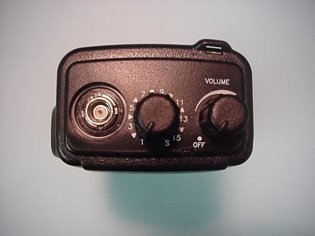
Photographs Front To p PTT Side Option Connector Side
ID Label/Location Info
FCC Label Drawing
ID Label/Location Info
Rear with FCC Label Location FCC ID Label Location
Internal Photos
PCB Top Side PCB Bottom Side
Operational Description
31 RPV599APlus Circuit Description 1. FREQUENCY CONFIGURATION The receiver utilizes double conversion. The first IF is 45.05 MHz and the second IF is 455KHz. The first local oscillator signal comes from the PLL circuit. The PLL circuit in the transmitter generates the necessary frequencies (See Fig.1). ANT IF SYSTEM SW RF AMP CF MIC 455KHZ MCF AF AMP TX AMP PA PLL SP VCO AMPAMP 12.8MHz MIC ANT Fig.1 2. RECEIVER SYSTEM The frequency configuration of the receiver is shown as following fig.2 ANT ANT SW BPF Q39 RF AMP L32 BPF L24,L26 MCF XF1 IF AMP Q21 MIXER Q29 CF1,2 IF,MIX,DET IC9 AF AMP IC12SP 1st Local OSC (PLL) 2nd Local OSC Fig.2 1) RF AMP The signal coming from the antenna passes through the transmit/receive switching diode circuit, passes through a BPF [L32], and is amplified by the RF amplifier [Q39]. The resulting signal passes through a BPF [L26] and goes to the mixer. 2) First mixer The signal from the front end is mixed with the first local oscillator signal generated in the PLL circuit by Q29 to produce a first IF frequency of 45.05 MHz. The resulting signal passes through the XF1 MCF to cut the adjacent spurious and provide the optimum characteristics, such as adjacent frequency selectivity. 32 3) IF amplifier The signal then passes through the first IF amplifier [Q21], and is amplified and goes to the IF IC (IC9). IC9 integrates the second OSC, second mixer, second IF amplifier, detector, noise amplifier, and noise detector. The signal input to the IC is mixed with the RF signal of the second OSC to produce a 455KHz second IF signal. The signal is amplified by the IF amplifier. The signal is switched by Wide/Narrow switch diode and then passes through the ceramic filters (CF1 and CF2) to provide the necessary selectivity. Finally, the signal is detected by the IC and output as an AF signal. 4) AF amplifier The AF signal from the IF IC is amplified by IC8 (1/2) and passes through the high-pass filter (Q25 and Q28) to remove 300 Hz and lower frequencies to suppress the sub-audio signal. The signal then passes through the de-emphasis circuit to restore the audio frequency characteristics. The signal passes through AF VOL and enters the IC12 audio power amplifier to drive the speaker.(See Fig.3) FM IF IC9 IF AMPDET DETHPFAMP IC8(1/2) AF AMPHPF Q30 SW IC12 AF PF AMP Q40 SW SP Q34,Q35,Q36 SW IC14 LPF 562676 BUSYMUTEAFCOTI IC403 MPU QT/DQT IC8(1/2) COMPALETER 2-TONE Q25,28 DTMF DETIC IC3 Fig.3 5) Squelch Part of the AF signal from the IC enters the FM IC again, and the noise component is amplified and rectified by a filter and an amplifier to produce a DC voltage corresponding to the noise level. The DC signal from the FM IC goes to the analog port of the microprocessor (IC1). IC1 determines whether to output sounds from the speaker by checking whether the input voltage is higher or lower than the preset value. To output sounds from the speaker, IC1 sends a high level to the MUTE and AFCO lines and turns IC12 on through Q30, Q35, Q34, Q36 and Q40. 6) Receive signaling (1) CTCSS 300Hz-and-higher audio frequencies of the signal output from IF IC are cut by a low-pass filter (IC14). The resulting signal enters the microprocessor (IC1). IC1 determines whether the CTCSS matches the preset value and controls the MUTE and AFCO and the speaker output sounds in line with the squelch results of that 33 content. (2) DTMF The part of the received AF signal passes through a high- pass filter (Q25 and Q28) and goes to IC3. IC3 detects a DTMF signal and sends received DTMF data to IC1. IC1 carries out various operations, such as sound output, according to the DTMF data. (See Fig.3) (3) 2-TONE Part of the receive AF signal output from the AF amplifier (IC8 1/2) goes to the other IC8 (1/2), is compared, and goes to IC1. IC1 checks whether 2-TONE data is necessary. If it matches, IC1 carries out a specified operation, such as turning the speaker on. 3. PLL The PLL circuit generates the first local oscillator signal for reception and the RF signal for transmission. 1) PLL The receiver has a VCO Q16, and the transmitter has another VCO (Q18). The generated signal passes through the Q20 buffer and Q14 amplifier and enters the IC6 PLL IC. IC6 incorporates the reference oscillation divider and phase comparator functions. The input signal is divided into a 2.5 or 6.25KHz signal according to divide ratio data from the microcomputer (IC1). This signal and the 2.5 or 6.25KHz signal divided from the reference signal enter the phase comparator to produce a differential signal. The frequency control signal is output from the charge pump. This signal passes through the passive LPF and goes to the varicap to control the VCO frequency (See Fig. 4). 123456 A B C D 6 54321 D C B A Title NumberRevisionSize B Date:15-Jul-2003Sheet of File:C:\Documents and Settings\yfwcy\×ÀÃæ\RPV599~3.DDBDrawn By: PLL DATA PLL IC IC8 I/N 5KHz/6.25KHz PHASE COMPARATOR REF OSC 12.8MHz I/M 5KHz/6.25KHz CHARGE LPF D7,9 Q18 TX VCO D8,10 Q16 RX VCO Q20 BUFF AMP VCO VOLTAGE Q14 RF AMP PUMP SELECT SW Fig.4 2) Reference Oscillator Circuit 34 The reference oscillator circuit in the PLL IC produces the 12.8MHz PLL reference frequency. To stabilize the frequency, the characteristics of the 12.8MHz crystal oscillator are controlled and the frequency is temperature- compensated. It is compensated for by changing the DC voltage applied to D4. Changes in the ambient temperature are input to the analog port of IC1 using the TH3 thermistor. IC1 judges the temperature and outputs a voltage to the TC1, TC2, or TC3 port. The temperature compensation value is corrected according to the differences in the characteristics of the thermistors in the TC1, TC2, and TC3 circuits. The temperature compensation is carried out when the temperature is -10 or less.(See Fig.5) D C B A EP CK DT TC3TC2TC1TC IN R52 CP3 C30C32C36 1120 IC6 CLOCKNCDATALEFCBISWFOUTPNCRXIN NC XOUT VP VCC DO GND LDNCFIN 10 1C28 D3R66 RF INPUT C31 C40 C39 L3 R56R58 X2 12.8MHz C240 C46 C45 TC1 C49 …
Text truncated - open the document above for the full version.
Parts List/Tune Up Info
60 Description of main component Ref. No. Parts NO. Description IC1 M3826AEFGP IC, MICRO PROCESSOR IC2 PST9140NR IC, RESET SWITCH IC3 LC73881M IC, DTMF DECODER IC4 AT24C32AN IC, EEPROM IC5 RN5VL45C IC, VOLTAGE DETECT IC6 LMX1511TMX IC, PHASE LOCKED LOOP SYSTEM IC7 S-81350HG-KD IC, VOLTAGE REGULATER IC8 TA75W01FU IC, AUDIO AMP ACTIVE FILTER IC9 TA31136FN IC, IF SYSTEM IC10 NJM2100V IC, AUDIO AMP IC11 RA07M4047M IC, RF POWER AMP IC11 RA07M1317M IC, RF POWER AMP IC12 TA7368F IC, AUDIO POWER AMP IC13 NJM2904V IC, APC IC14 TA75W01FU IC, ACTIVE FILTER Q1~Q3 DTC114EE TRANSISTOR, DC SWITCH Q4 DTC114YE TRANSISTOR, CLOCK FREQUENCY SHIFT Q5 UMG3N TRANSISTOR, DC SWITCH Q6 UPA572T FET, DC SWITCH Q8 FMMT591 TRANSISTOR, DC SWITCH Q9 UMG3N TRANSISTOR, DC SWITCH Q12 DTA114YE TRANSISTOR, DC SWITCH Q14 2SC4619 TRANSISTOR, RF AMP Q15 DTA114EE TRANSISTOR, AF MUTE SWITCH Q16 2SK1875(V) FET, VCO RX Q17 2SC4617(S) TRANSISTOR, ACTIVE FILTER Q18 2SK1875(V) TRANSISTOR, VCO TX 61 Q19 2SJ243 FET, DC SWITCH Q20 2SC5108(Y) TRANSISTOR, RF BUFFER AMP Q21 2SC5108(Y) TRANSISTOR, IF AMP Q22 2SC4617(S) TRANSISTOR, ACTIVE FILTER Q23 UMC4 TRANSISTOR, DC SWITCH Q24 2SC4617(S) TRANSISTOR, RIPPLE FILTER Q25 2SC4617(S) TRANSISTOR, ACTIVE FILTER Q26 2SC5108(Y) TRANSISTOR, RF AMP Q28 2SC4617(S) TRANSISTOR, ACTIVE FILTER Q29 3SK320 FET, MIXER Q30 2SK1824 FET, AUDIO MUTE SWITCH Q31 2SC4988 TRANSISTOR, TX DRIVE Q32 DTA144EE TRANSISTOR, AUDIO MUTE SWITCH Q34 2SA1362(GR) TRANSISTOR, DC SWITCH Q35, Q36 DTC144EE TRANSISTOR, DC SWITCH Q37 2SC4919 TRANSISTOR, AUDIO MUTE SWITCH Q38 DTC114EE TRANSISTOR, DC SWITCH Q39 2SK1215(E) FET, RF AMP Q40 2SK1588 FET, AUDIO MUTE SWITCH Q41 DTA144EE TRANSISTOR, DC SWITCH D1 CL-220YG LED, LCD BACKLIGHT D2 UN-WMV-SRGC LED, TX BUSY LED D3 MA2S111 DIODE, UNLOCK DETECT D4 1SV269 VARIABLE CAPACITANCE DIODE, FREQUENCY CON D5 1SS373 DIODE, REVERSE-FLOW PREVENTION D6 UMN1N DIODE, DC CUT D7~D10 1SV283 VARIABLE CAPACITANCE DIODE, FREQUENCY CON D11 1SV214 VARIABLE CAPACITANCE DIODE, TX MODULATION D14 MA2S111 DIODE, CURRENT STEERING D15 DA221 DIODE, LIMITTER D16,D17 MA2S077 DIODE, RF SWITCH D19 1SS372 DIODE, AGC DETECT D20 MA8062 ZENER DIODE, VOLTAGE PROTECTION D21 DAN222 DIODE, REVERCE PROTECTION D22 HVU131 DIODE, ANT SWITCH D23 MA2S077 DIODE, ANT SWITCH D24 1SR154-400 DIODE, REVERCE PROTECTION Q300 DTA144EE TRANSISTOR, DC SWITCH Q301 2SK1824 TRANSISTOR, DC SWITCH Q302 DTA144EE TRANSISTOR, DC SWITCH Q303 DTC144EE TRANSISTOR, DC SWITCH Q304 DTC144EE TRANSISTOR, DC SWITCH
Parts List/Tune Up Info
45 RPV599APlus Adjustment Description Required Test Equipment Stabilized Power supply 1. The supply voltage can be changed between 5V and 8V, and the current is 3A or more. 2. The standard voltage is 7.5V. DC Ammeter 1. Class 1 ammeter (17 ranges and other features). 2. The full scale can be set to either 300mA or 3A. 3. A cable of less internal loss must be used. Digital Voltmeter 1. Voltage range: FS=18V or so 2. Input resistance: 1MΩ or more Oscilloscope 1. Measuring range: DC to 30MHz 2. Provides highly accurate measurements for 5 to 25MHz. Dummy Load 8Ω, 3W or more RADIO COMMUNICATION TESTER 2955B Spectrum Analyzer SG815 Initialization: The model of RPV599APlus is 8. Frequency range is 148-174MHz. Notes: 1. Use a non-conductive rod such as a Bakelite rod for adjustment (especially of trimmers and coils) 2. When adjusting receiver unit, do not send signal. Then the standard signal generator can be protected. 3. The output level of standard signal generator is the maximum. Adjustment specifications: TC1: Frequency adjustment TC2: Receive lock voltage adjustment TC3: Transmit lock voltage adjustment VR1: CTCSS/CDCSS waveform adjustment VR2: DEV adjustment L24: L26: B.P.F waveform adjustment L32: TP: B.P.F test point ANT: Antenna connector SP: Speaker jack MIC: Microphone jack CH: Channel selector VR3: DTMF/TTS DEV adjustment Key: DTMF9 key terminal 9 46 CV: Lock voltage test terminal Use the jig as the following: 1. Insert the coaxial antenna connector into the jig. 2. Place the unit on the jig and fix it with four screws. 3. Solder the antenna terminal to the terminal of the unit. Notes: 1. Do not install the Ni-Cd battery when using the jig for adjustment, repair, or checking. If the Ni-Cd battery is installed, the relay terminal (+) may be damaged. 2. Using an external power supply as the radio power. 3. Please refer to the “adjustment mode” in “Radio Modes” to adjust. RPV599APlus VCO adjustment RPV 599APlus Receiver adjustment Fig.9 Measurement Adjustment Item Condition Test equipment Terminal Parts Method Specifications/R emarks 1.Setting Power supply voltage Battery terminal: 7.5V 1) TX HI Digital voltmeter CV TC3 3.8 ±0.1V 2) TX LOW Digital voltmeter CV ≥0.7V Check 3) RX HI Digital voltmeter CV TC2 3.8 ±0.1V 2.VCO lock voltage 4) RX LOW Digital voltmeter CV ≥0.8V Check 47 RPV599APlus Transmitter adjustment Measurement Adjustment Item Condition Test equipment Terminal Parts Method Specifications/R emarks 1. Band-pass filter 1) Given frequency 2) Trapezium generator output – 40 dBm. Connect the spectrum analyzer to the T.P terminal. Trapezium generator Spectrum analyzer ANT TP L24 L26 L32 Adjust the frequency so that it becomes the spectrum waveform shown above Fig.(See Fig. 9) 2. Sensitivity CH: RX LO CH: RX Center CH: RX HI At each frequency: SSG output: -121dBm MOD: 1KHz DEV:±3KHz SSG Oscilloscope AF.V.M Distortion meter ANT SP Check SINAD: 12dB or higher 3. Signal-to- Noise SSG output 66dBμV Check ≥40 dB 4. Distortion S S G o u t p u t 6 6 d B μ V C h e c k ≤3.5% 1) Level 9 CH: RX Center SSG output: -117dBm Level 9 Adjust to close the squelch with the channel selector. Squelch must be closed. 2) Level 3 CH: RX Center SSG output:: -128dBm 5.Squelch 3) Refer to adjustment mode. SSG Oscilloscope AF.V.M Distortion meter ANT S.P Channel selector Level 3 Adjust to close the squelch with the channel selector. Squelch must be closed. Measurement Adjustment Item Condition Test equipment Terminal Parts Method Specifications/R emarks 1.Transmit frequency 1) CH: TX Center PTT: ON Frequency counter ANT TC1 Adjust to ±200 Hz. Within ±200Hz 1) Refer to adjustment mode. CTCSS is 67Hz. 67Hz CTCSS 2. CTCSS/ CDCSS Balance 2) Refer to adjustment mode. CTCSS is 250.3Hz. LPF: 300Hz Modulation analyzer or linear detector Oscilloscope ANT VR1 Adjust VR1 to make the frequency deviation of 67Hz consistent with that of 250.3Hz 250.3Hz CTCSS 1) CH: TX Center Battery terminal: 7.5V PTT: ON 3. Full Power 2) Refer to adjustment mode Power meter Ammeter ANT Channel selector Turn the channel selector to increase the value. Verify that it is 5W or higher 5W or higher 1) CH: TX Center Battery terminal: 7.5V PTT: ON 2) Refer to adjustment mode. Adjust it to 5W ± 0.1W with the channel selector. 5W± 0.1W 2.0A or lower 4. High Power 3) CH: TX HI, Lo Battery terminal: 7.5V PTT: ON Power meter Ammeter ANT Channel selector Check ≥4.5W 2.0A or lower 48 1) CH: TX Center, LO PTT: ON 2) Refer to adjustment Mode. Adjust it to 1.0W ± 0.1W with the channel selector. 1.0 ± 0.1W 1.0A or lower 5.Low power 3) CH: TX HI, Lo PTT: ON Power meter Amperometer ANT Channel selector C h e c k 0.5~ 1.5W 1) CH: TX HI 2) Low-frequency oscillator output: 1 KHz 50mV PTT:ON Adjust it to±4KHz±100Hz MOD METER L.P.F 15KHz 4. 0KHz ±100Hz 6.Modulation 3) CH: TX Center Low-frequency oscillator output 20 dBm 1KHz: 10mV Modulation analyzer or linear detector Oscilloscope Low-frequency oscillator AF.V.M. ANT MIC VR2 Check ±2.2KHz ~±3.6KHz 7. Modulation distortion Low-frequency oscillator output 1KHz: 10mV Check ≤3.5% 8.Transmit S/N CH: TX Center HPF: 300Hz LPF: 3KHz DEMP: 750μs Modulation analyzer or linear detector Oscilloscope Low-frequency oscillator AF.V.M ANT MIC Check 40dB or higher 1) CH: TX Center 2) CTCSS: 151.4Hz 9.CTCSS DEV (wideband) 3) Refer to adjustment mode (wideband). LPF: 300Hz Modulation analyzer or linear detector Oscilloscope Low-frequency oscillator AF.V.M ANT MIC Channel selector Adjust it to 0.7KHz±50Hz with the channel selector. 0.7KHz ±50Hz 1) CH: TX Center 2) CDCSS: 023 10.CDCSS DEV (wideband) 3) Refer to adjustment mode (wideband). LPF: 300Hz Modulation analyzer or linear detector Oscilloscope Low-frequency oscillator AF.V.M ANT MIC Channel selector Adjust it to 0.7KHz±50Hz with the channel selector. 0.7KHz ±50Hz 1) CH: TX Center 2) CTCSS: 151.4Hz 11.CTCSS DEV (narrowband) 3) Refer to adjustment mode (wideband). LPF: 300Hz Modulation analyzer or linear detector Oscilloscope Low-frequency oscillator AF.V.M ANT MIC Channel …
Text truncated - open the document above for the full version.
RF Exposure Info
© 2004 Celltech Labs Inc. 1 of 20 Test Report S/N: 040704-499ARU Test Date(s): March 09 & April 07, 2004 Test Type: FCC/IC SAR Evaluation Celltech Labs Inc. declares under its sole responsibility that this wireless portable device has demonstrated compliance with the Specific Absorption Rate (SAR) RF exposure requirements specified in FCC 47 CFR §2.1093 and Health Canada’s Safety Code 6. The device was tested in accordance with the measurement standards and procedures specified in FCC OET Bulletin 65, Supplement C (Edition 01-01) and Industry Canada RSS-102 Issue 1 (Provisional) for the Occupational / Controlled Exposure environment. All measurements were performed in accordance with the SAR system manufacturer recommendations. I attest to the accuracy of data. All measurements were performed by me or were made under my supervision and are correct to the best of my knowledge and belief. I assume full responsibility for the completeness of these measurements and vouch for the qualifications of all persons taking them. This test report shall not be reproduced partially, or in full, without the prior written approval of Celltech Labs Inc. The results and statements contained in this report pertain only to the device(s) evaluated. Russell W. Pipe Senior Compliance Technologist Celltech Labs Inc. DECLARATION OF COMPLIANCE SAR RF EXPOSURE EVALUATION Test Lab CELLTECH LABS INC. Testing and Engineering Services 1955 Moss Court Kelowna, B.C. Canada V1Y 9L3 Phone: 250-448-7047 Fax: 250-448-7046 e-mail: [email protected] web site: www.celltechlabs.com Applicant Information RELM COMMUNICATIONS INC. 7100 Technology Drive West Melbourne, Florida 32904 Rule Part(s): FCC 47 CFR §2.1093; IC RSS-102 Issue 1 (Provisional) Test Procedure(s): FCC OET Bulletin 65, Supplement C (Edition 01-01) Device Classification: Licensed Non-Broadcast Transmitter Held to Face (TNF) Device Type: Portable FM UHF PTT Radio Transceiver FCC IDENTIFIER: ARURPU499A Model(s): RPU499A Modulation: FM (UHF) Tx Frequency Range: 450.0 - 470.0 MHz Max. RF Output Power Tested: 4.25 Watts Conducted (450.0 MHz) 4.22 Watts Conducted (460.0 MHz) 4.39 Watts Conducted (470.0 MHz) Antenna Type(s) Tested: Whip Battery Type(s) Tested: NiMH 7.2 V, 1600 mAh Body-Worn Accessories Tested: Plastic Belt-Clip, Speaker-Microphone Max. SAR Levels Measured: 2.63 W/kg - Face-held (50% Duty Cycle) 5.50 W/kg - Body-worn (50% Duty Cycle) © 2004 Celltech Labs Inc. 2 of 20 Test Report S/N: 040704-499ARU Test Date(s): March 09 & April 07, 2004 Test Type: FCC/IC SAR Evaluation TABLE OF CONTENTS 1.0INTRODUCTION.....................................................................3 2.0DESCRIPTION OF DUT............................................................ 3 3.0SAR MEASUREMENT SYSTEM................................................ 4 4.0MEASUREMENT SUMMARY..................................................... 5 5.0DETAILS OF SAR EVALUATION............................................... 6 6.0EVALUATION PROCEDURES................................................... 6 7.0SYSTEM PERFORMANCE CHECK............................................. 7 8.0SIMULATED EQUIVALENT TISSUES.......................................... 8 9.0SAR SAFETY LIMITS............................................................... 8 10.0ROBOT SYSTEM SPECIFICATIONS........................................... 9 11.0PROBE SPECIFICATION.......................................................... 10 12.0PLANAR PHANTOM................................................................. 10 13.0VALIDATION PHANTOM........................................................... 10 14.0DEVICE HOLDER.................................................................... 10 15.0TEST EQUIPMENT LIST............................................................ 11 16.0MEASUREMENT UNCERTAINTIES............................................. 12-13 17.0REFERENCES.........................................................................14 APPENDIX A - SAR MEASUREMENT DATA............................................... 15 APPENDIX B - SYSTEM PERFORMANCE CHECK DATA............................ 16 APPENDIX C - SYSTEM VALIDATION PROCEDURES................................. 17 APPENDIX D - PROBE CALIBRATION...................................................... 18 APPENDIX E - MEASURED FLUID DIELECTRIC PARAMETERS................... 19 APPENDIX F - SAR TEST SETUP & DUT PHOTOGRAPHS.......................... 20 © 2004 Celltech Labs Inc. RELM Communications Inc. FCC ID: ARURPU499A 3 of 20 Portable FM UHF PTT Radio Transceiver (450-470 MHz) Test Report S/N: 040704-499ARU Test Date(s): March 09 & April 07, 2004 Test Type: FCC/IC SAR Evaluation This measurement report demonstrates that the RELM Communications Inc. Model: RPU499A Portable FM UHF PTT Radio Transceiver FCC ID: ARURPU499A complies with the SAR (Specific Absorption Rate) RF exposure requirements specified in FCC 47 CFR §2.1093 (see reference [1]), and Health Canada’s Safety Code 6 (see reference [2]) for the Occupational / Controlled Exposure environment. The measurement procedures described in FCC OET Bulletin 65, Supplement C (Edition 01-01) (see reference [3]) and IC RSS-102 Issue 1 (Provisional) (see reference [4]), were employed. A description of the product, operating configuration, detailed summary of the test results, methodology and procedures used in the evaluation, equipment used, and the various provisions of the rules are included within this test report. FCC Rule Part(s) 47 CFR §2.1093 IC Rule Part(s) RSS-102 Issue 1 (Provisional) Test Procedure(s) FCC OET Bulletin 65, Supplement C (01-01) Device Type Portable FM UHF PTT Radio Transceiver FCC IDENTIFER ARURPU499A Model(s) RPU499A Serial No. 03D31B0002 (Identical Prototype) Modulation FM (UHF) Tx Frequency Range 450.0 - 470.0 MHz 4.25 Watts Conducted 450.0 MHz 4.22 Watts Conducted 460.0 MHz Max. RF Output Power Tested 4.39 Watts Conducted 470.0 MHz Antenna Type(s) Tested Whip (Length: 160 mm) Battery Type(s) Tested NiMH (7.…
Text truncated - open the document above for the full version.
Schematics
PRV599A 7 Schematic Diagram (To Be Updated)
Test Report
TIMCO ENGINEERING INC. 849 NW State Road 45 Newberry, Florida 32669 http://www.timcoengr.com 888.472.2424 F 352.472.2030 email: [email protected] APPLICANT: RELM WIRELESS CORPORATION FCC ID: ARURPU499A REPORT #: R\RELM_ARU\191AUT4\191AUT4TestReport.doc COVER SHEET Test Report Product Name: UHF LAND MOBILE RADIO FCC ID: ARURPU499A Applicant: RELM WIRELESS CORPORATION 7100 TECHNOLOGY DRIVE W. MELBOURNE, FLORIDA 32904 DBA RELM COMMUNICATIONS INC. Date Receipt: FEBRUARY 17, 2004 Date Tested: FEBRUARY 26, 2004 TIMCO ENGINEERING INC. 849 NW State Road 45 Newberry, Florida 32669 http://www.timcoengr.com 888.472.2424 F 352.472.2030 email: [email protected] APPLICANT: RELM WIRELESS CORPORATION FCC ID: ARURPU499A REPORT #: R\RELM_ARU\191AUT4\191AUT4TestReport.doc TABLE OF CONTENTS TABLE OF CONTENTS LIST APPLICANT: RELM WIRELESS CORPORATION FCC ID: ARURPU499A TEST REPORT: PAGE 1...........GENERAL INFORMATION & TECHNICAL DESCRIPTION PAGE 2...........TECHNICAL DESCRIPTION CONTINUED RF POWER OUTPUT PAGE 3...........MODULATION CHARACTERISTICS AUDIO FREQUENCY RESPONSE PAGE 4...........MODULATION LIMITING PLOT PAGE 5...........AUDIO LOW PASS FILTER PAGE 6-7.........OCCUPIED BANDWIDTH PAGE 8-11........OCCUPIED BANDWIDTH PLOTS PAGE 12..........SPURIOUS EMISSIONS AT ANTENNA TERMINALS METHOD OF MEASURING SPURIOUS EMISSIONS AT ANTENNA TERMINALS PAGE 13-15.......FIELD STRENGTH OF SPURIOUS EMISSIONS PAGE 16..........METHOD OF MEASURING RADIATED SPURIOUS EMISSIONS PAGE 17..........FREQUENCY STABILITY PAGE 18-19.......TRANSIENT FREQUENCY STABILITY PAGE 20-21.......TRANSIENT FREQUENCY RESPONSE GRAPHS PAGE 22-25.......EQUIPMENT LIST EXHIBITS CONTAINING: BLOCK DIAGRAM SCHEMATIC PARTS LIST USERS MANUAL LABEL SAMPLE LABEL LOCATION EXTERNAL PHOTOGRAPHS INTERNAL PHOTOGRAPHS ALIGNMENT PROCEDURE OPERATIONAL DESCRIPTION TEST SET UP PHOTOGRAPH TIMCO ENGINEERING INC. 849 NW State Road 45 Newberry, Florida 32669 http://www.timcoengr.com 888.472.2424 F 352.472.2030 email: [email protected] APPLICANT: RELM WIRELESS CORPORATION FCC ID: ARURPU499A REPORT #: R\RELM_ARU\191AUT4\191AUT4TestReport.doc Page 1 of 25 GENERAL INFORMATION REQUIRED FOR TYPE ACCEPTANCE 2.1033(c)(1)(2) RELM WIRELESS CORPORATION will manufacture the FCCID: ARURPU499A VHF TRANSCEIVER in quantity, for use under FCC RULES PART 90. RELM WIRELESS CORPORATION 7100 TECHNOLOGY DRIVE W. MELBOURNE, FLORIDA 32904 2.1033(c) TECHNICAL DESCRIPTION 2.1033(c)(3) Instruction book. A draft copy of the instruction manual is included in the exhibits. 2.1033(c) (4) Type of Emission: 9K8F3E 90.209 Bn = 2M + 2DK M = 3000 D = 2500 Bn = 2(3000)+2(1900) = 9.8k 90.209 Authorized Bandwidth 11.25 kHz 2.1033(c) (4) Type of Emission: 13K0F3E 90.209 Bn = 2M + 2DK M = 3000 D = 5000 Bn = 2(3000)+2(2500) = 13k 90.209 Authorized Bandwidth 20 kHz 2.1033(c)(5) Frequency Range: 450 - 470 MHz 90.209 90.203 This equipment meets the requirements of the FCC Rules, Part 90.203(e) except as provided in paragraph (g) of the section 203. The operator cannot program and transmit on frequencies other than those programmed by the manufacturer, service or maintenance personnel, using the equipment’s external operational controls. 2.1033(c)(8) DC Voltages and Current into Final Amplifier: POWER INPUT: FINAL AMPLIFIER ONLY INPUT POWER – HIGH: (7.2V)(0.750A) = 5.4 Watts TIMCO ENGINEERING I…
Text truncated - open the document above for the full version.
Contact Information
Applicant
Walter C. Simciak(Engineering Manager)
Test Firm
Timco Engineering, Inc.S Sanders
Technical Specifications
| # | Rule Parts | Frequency Range | Power Output | Emission | Tolerance |
|---|---|---|---|---|---|
| 4 | 22,74,80,9 | 450 MHz - 470 MHz | 1 W | 16K0F3E | 2.5 ppm |
Other Applications from RELM Communications Inc
ARURPU416B
Dec 15, 2004UHF Transceiver
Equipment Class
TNF - Licensed Non-Broadcast Transmitter Held to Face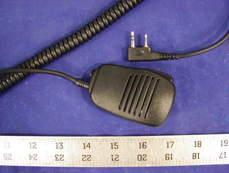
ARURPV599A
Dec 22, 2002VHF FM Transceiver
Equipment Class
TNF - Licensed Non-Broadcast Transmitter Held to Face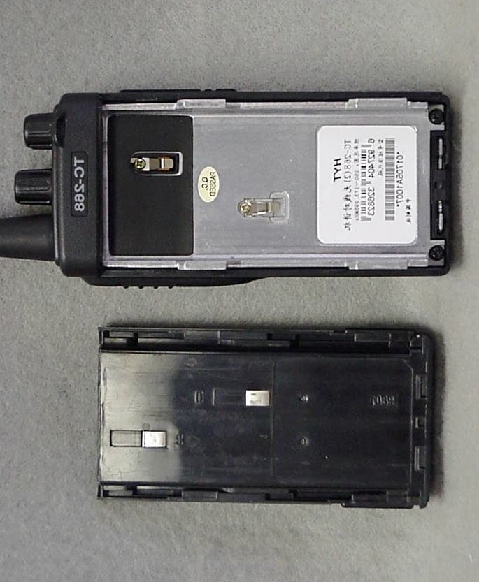
ARURPV516A
Jan 03, 2002VHF FM Transceiver
Equipment Class
TNF - Licensed Non-Broadcast Transmitter Held to Face
ARUSRU50ABC
Jan 25, 1999Repeater
Equipment Class
TNB - Licensed Non-Broadcast Station Transmitter
ARUSRE35AB
Oct 06, 1998TNB - Licensed Non-Broadcast Station Transmitter
Equipment Class
TNB - Licensed Non-Broadcast Station Transmitter